User's Guide
SLVUA18 – January 2014
bq24230H and bq24232H 0.5-A Single-Chip Li-Ion
This user’s guide describes the bq24230H (PREVIEW) and bq24232H (bqTINY-III™) evaluation module
(EVM). The EVM provides a convenient method for evaluating the performance of a charge management
and system power solution for portable applications having 4.35-V Li-Ion batteries using either the
bq24230H and bq24232H products. A completely designed and tested module is presented. The charger
is designed to deliver up to 0.5 A of continuous current to the system or charger for one-cell Li-ion or Lipolymer applications (see the data sheet for the correct device) using a DC power supply. The charger is
programmed by the factory to deliver 0.5 A of charging current. This EVM was designed as a standalone
evaluation module, but it can also be interfaced with the system and host via the connectors and headers.
1
2
3
4
5
Contents
Introduction .................................................................................................................. 2
1.1
References .......................................................................................................... 3
1.2
Schematic ........................................................................................................... 3
Performance Specification Summary ..................................................................................... 3
2.1
Performance Recommendations ................................................................................. 4
Test Summary ............................................................................................................... 4
3.1
Equipment ........................................................................................................... 4
3.2
Equipment and EVM Setup ....................................................................................... 4
3.3
Test Procedure ..................................................................................................... 6
Physical Layouts ............................................................................................................ 8
4.1
Board Layout ....................................................................................................... 8
Bill of Materials ............................................................................................................. 10
List of Figures
1
Test Diagram ................................................................................................................
5
2
Modes of Operation Tested in Steps 11 Through 13
..................................................................
7
3
Charge Enabled, Pulled High, Then Low – Disables Charge .........................................................
7
4
Top Assembly View .........................................................................................................
8
5
Board Layout – Top Etch Layer ...........................................................................................
8
6
Board Layout – Bottom Etch Layer .......................................................................................
9
List of Tables
1
Ordering Information ........................................................................................................
2
2
Performance Specification Summary for bq24230H and bq24232H EVMs .........................................
3
3
bq2423XHEVM Jumpers ...................................................................................................
4
SLVUA18 – January 2014
Submit Documentation Feedback
bq24230H and bq24232H 0.5-A Single-Chip Li-Ion
Copyright © 2014, Texas Instruments Incorporated
1
�Introduction
1
www.ti.com
Introduction
The bq2423xH family powers the system while independently charging the battery. This feature reduces
the charge and discharge cycles on the battery, allows for proper charge termination, and allows the
system to run with an absent or defective battery pack. This feature also allows for the system to
instantaneously turn on from an external power source even when using a deeply discharged battery
pack.
This charger family has one input and can be programmed to be used with an adapter or USB port as the
power source for the system. In the USB configuration, the host can select from the two preset input
maximum current limits of 100 and 500 mA. The charger dynamically adjusts the charge rate based on
the system load to stay within the 100-mA or 500-mA maximum limits. An external resistor, RSET1, sets
the magnitude of the charge current between 25 and 500 mA. If the charge current exceeds the available
input current, the voltage on the OUT pin drops to the DPPM threshold or the battery voltage, whichever is
higher. The charging current is reduced to what current is available (IBAT = IIN – IOUT).
The integrated circuit (IC) charges the battery in three phases: conditioning, constant current, and
constant voltage. Charge is terminated based on minimum current. A resistor-programmable charge timer
provides a backup safety for charge termination. The charge automatically restarts if the battery voltage
falls below an internal threshold. Sleep mode is entered when the supply is removed (Vin drops to the
battery voltage). Pin 15 of bq24230H has a TD pin that allows the user to disable termination (as well as
safety timers) at startup. Pin 15 of the bq24232H is ITERM, which allows the user to set the termination up
to 50% of the fast charge current instead of the default 10% value.
Table 1. Ordering Information
Part Number
VOVP
VBAT
VOUT(REG)
VDPM
Optional Function
(PIN 15)
Marking
bq24230HRGTR
(PREVIEW)
6.6 V
4.35 V
4.5 V
VO(REG) – 100 mV
TD
24230H
bq24232HRGTT
10.5 V
4.35 V
4.5 V
VO(REG) – 100 mV
ITERM
24232H
The two potential sources to power the system (VOUT) are the input source and the battery (adapter or
USB port). The IC is designed to power the system continuously. If the adapter or USB input is not
available (or disabled), the battery connects to the system.
In the thermal regulation condition (TJ = 125°C, not a first-choice design mode of operation), the charge
current is reduced to the battery, and the system still gets its power from the input. The battery
supplement is available in thermal regulation if the VOUT falls to VBAT. In thermal cutoff (approximately
155°C), the input sources are disconnected, but the internal battery FET connects the battery to VOUT.
bqTINY-III is a trademark of Texas Instruments.
2
bq24230H and bq24232H 0.5-A Single-Chip Li-Ion
Copyright © 2014, Texas Instruments Incorporated
SLVUA18 – January 2014
Submit Documentation Feedback
�Performance Specification Summary
www.ti.com
1.1
References
bq24230H and bq24232H data sheet, USB-Friendly Li-Ion Battery Charger and Power-Path Management
IC, TI literature number SLUS821
1.2
Schematic
D1 Red
JP6
R5
1.5 kΩ
1
LED
2
\CHG
D2
Green
JP7
R6
2
1.5 kΩ
1
LED
2
\PGOOD
5 kΩ
TP12
TP10
J2
R1
13
PGOOD
15
EN1
ISET
EN2
17
EXT PGM
TMR
2
All TMRs Disabled - GNDed
GND
3
INT FIXed TMR - No Shunt
TP14
LO (GND)
3
J3
TP16
R9
0Ω
TP15
10 kΩ
R23
BAT–
1
TS
J4
10 µF
0Ω
1
VSS
R10
BAT–
R19
11 kΩ
4
10 kΩ
BAT+
2
2
R16
50 kΩ
C3
Normal_MODE
G15
1
1
R7
1 LDO_MODE
TD/ITERM/SYSOFF
R22
23.7 kΩ
TP1
HI15
JP2
2
5
TP2
49.9 kΩ
G14
HI (OUT)
6
IN
TS
R4
1
1
JP1
RESISTOR
7
PWRPD
BZX84C6v2T
P14
U1
TD
16
8
CE
C1
10 µF
D3
BAT
R17
1 kΩ
OUT
VSS
TMR
4
C4
GND
10 µF
6
IN
14
10 µF
CHG
ILIM
IN
3
2
OUT
1
BAT
IN (DC+)
GND (DC_)
OUT
1
C2
TP13
604 Ω
2
J1
10
R20
2
9
732 Ω
12
5
11
R8
R21
1.5 kΩ
R11
R2
1 kΩ
10 kΩ
5
R18
604
HI4
JP3
R12
1
HI (OUT)
TP4
10k
2
\CE
CE
3
LO (GND)
G16
TS
G4
R13
1
HI (OUT)
R3
10 kΩ
HI5
JP4
EN2
2
LO (GND)
3
TP5
5
10 kΩ
EN2
G5
R14
301 kΩ
HI6
JP5
HI (OUT)
EN1
LO (GND)
R15
1
TP6
10 kΩ
2
EN1
3
G6
VSS
2
Performance Specification Summary
Table 2 summarizes the performance specifications of the EVM.
Table 2. Performance Specification Summary for bq24230H and bq24232H EVMs
MIN
TYP
Input DC Voltage for bq24230H, VIN
SPECIFICATION
TEST CONDITIONS
4.75
5
6.4
Input DC Voltage for bq24232H, VIN
4.75
5
10.2
V
250
500
mA
See (1)
W
Battery Charge Current, ICHG
Power Dissipation, bq24230H and bq24232H IC, 1 Cell Pdiss = (VIN – VOUT) IOUT + (VIN – VBAT) IBAT
(1)
MAX UNIT
V
+
The PCB thermal design is optimized (8 vias, 0.031-inch PCB, 2-oz. copper) to give
θJA ≈ 27°C/W.
SLVUA18 – January 2014
Submit Documentation Feedback
bq24230H and bq24232H 0.5-A Single-Chip Li-Ion
Copyright © 2014, Texas Instruments Incorporated
3
�Test Summary
2.1
www.ti.com
Performance Recommendations
This IC is a linear battery charger and also powers the system from the input through the linear regulator
output. Being a linear device, the charger is most efficient when the input voltage is only slightly above the
battery voltage (VIN = 4.75 to 5.5 V). Too low of an input voltage (less than the OUT voltage plus the
dropout voltage) results in degraded performance. Excessive input voltage (> 5.5 V) results in excess
power dissipation and reduced performance (that is, reduced charge current) due to the IC's thermal
regulation protection circuit. The IC is rated to 28 V and is not damaged with VIN voltages less than this,
but any VIN voltage over the overvoltage protection (OVP) threshold disables the IC. Thus, the
recommended operating range for maximum performance is between 4.75 and 5.5 V, with a preference
for the lower values.
3
Test Summary
This section covers the setup and tests performed in evaluating the EVM.
3.1
Equipment
•
•
•
3.2
Power supply (+5.25 ±0.25 Vdc), current limit set to 1 A ±0.1 A
Three Fluke 75 DMMs (equivalent or better)
Oscilloscope, model TDS220 (equivalent or better)
Equipment and EVM Setup
•
•
•
•
•
Preset P/S number 1 to 5.25 V ±0.25 V, 2 A ±0.25-A current limit, turn off, and connect to J1-IN/GND
(+ to IN and – to GND)
Connect a 10-Ω, 10-W resistor to J2-OUT/VSS
Connect a fully discharged (VBAT < 2.8 V) Battery to J3-BAT+/VSS (+ to BAT+ and – to VSS)
Apply the jumpers as per Table 3
For the bq2423xEVM, adjust the potentiometers as follows (measure resistance from TP number to
VSS):
– R8 (ILIM-TP12) = 3.1 kΩ (3.07 to 3.13 kΩ)
– R11 (ISET-TP16) = 1.74 kΩ (1.72 to 1.75 kΩ)
– R16 (TS-TP1) = 7.5 kΩ (7.3 to 7.7 kΩ)
– For bq24074 (-006): R10 (ITERM-TP15) = 3 kΩ (2.98 to 3.02 kΩ)
Table 3. bq2423XHEVM Jumpers
4
Jumper
bq24230H
bq24232H
JMP1
RES–TMR
RES–TMR
JMP2
TD–Vss
TD–Vss
JMP3
CE–Vss
CE–Vss
JMP4
EN2–HI
EN2–HI
JMP5
EN1–Vss
EN1–Vss
bq24230H and bq24232H 0.5-A Single-Chip Li-Ion
Copyright © 2014, Texas Instruments Incorporated
SLVUA18 – January 2014
Submit Documentation Feedback
�Test Summary
www.ti.com
CH 2
5.25 VDC
DMM
#2
VSS
J2
R8-ILIM
OUT
R1
10 W
J1
IN
GND
PWR608
P/S
#1
CH 1
EN1
JMP5
TMR
EN2
JMP2
R10-ITERM R11-ISET
TD
JMP4
DMM
#1
CH 3
CE
JMP3
J3
4.2 V Li-Ion Cell
VSS = GND
VSS
BAT+
TS
R16-TS
VSS
J4
JMP2
DMM
#3
R2
0.1 W
CH 4
Figure 1. Test Diagram
SLVUA18 – January 2014
Submit Documentation Feedback
bq24230H and bq24232H 0.5-A Single-Chip Li-Ion
Copyright © 2014, Texas Instruments Incorporated
5
�Test Summary
3.3
www.ti.com
Test Procedure
1.
2.
3.
4.
Verify that the equipment and EVM is setup according to the preceding section.
Verify that VOUT is approximately equal to VBAT.
Turn on P/S number 1, +5.25-Vdc supply to the UUT.
Verify VBAT is between 2.4 and 3 Vdc, and the charger is in precharge state: LEDs CHG (D1) and
PGOOD (D2) are on. If VBAT is above the low-voltage threshold (V(LOWV) approximately 3 V), then the IC
is in fast-charge mode. If the IC is in fast charge, skip step 7.
5. Verify DMM number 3, IBAT is approximately 5 mV or approximately 0.05 A.
6. Verify that VOUT for bq2423XH is 4.4 to 4.6 V.
7. Allow the battery to charge until VBAT is between 3.3 and 4 Vdc. The charger delivers the programmed
constant current to the battery unless the input cannot source the required current.
8. Verify IBAT is approximately 50 mV or approximately 0.5 A (for a 1.74-kΩ resistor on ISET).
9. Set JMP5 (EN1) to HI, and verify that the chip is disabled, D1 (CHG) is turned off, and the P/S number
1 current has dropped to 0. The internal battery FET must be on, connecting the BAT pin to the OUT
pin. Verify that the voltage on the OUT pin is close to the battery voltage. See Figure 2 for EN1/2
modes of operation.
10. Set JMP4 (EN2) to VSS. Verify that the input current is less than 500 mA (USB 500-mA mode). If the
input current is restricted due to USB mode, or if the adapter is current limiting, the OUT pin drops in
voltage and enters the DPM mode, if the system current is less than the restricted input current. This
IC must be in DPM mode with the system voltage at the DPM.
11. Set JMP5 (EN1) to VSS and verify USB 100-mA mode. The system load is more than the allowed 100
mA on the input, so the OUT voltage drops to the battery voltage, and the battery FET is switched on
and supplements the input current. Verify that VOUT has dropped just below the battery voltage and the
battery is supplying IBAT, approximately (VOUT / 10 Ω – 100 mA).
12. Set JMP4 (EN2) to HI to return to the ISET mode where the programmed current is approximately
0.5 A.
13. Set JMP3 to HI, and verify that the charging is disabled and that the CHG LED (D1) turns off. Verify
that the system is still powered by the input.
14. Set JMP3 to VSS, and verify that charging continues and that D1 turns on.
15. Record the OUT voltage and battery charge current. Adjust R8 CCW until the input current starts to be
reduced (about 2 turns). Note how the OUT voltage drops and the charge current is reduced as the
input current limit loops kicks in and limits the input current. Adjust R8 to its original position.
16. On the bq24230H IC, set JMP2 HI, and verify that the BAT FET turns off and allows no charging or
discharging of the battery.
17. Adjust the R16 (TS-Pot) up or down until the TS threshold is reached. Verify that the charging current
is disabled. Return the TS resistance within the normal range and verify the continued charging
operation.
18. Allow the battery to continue to charge until the battery reaches voltage regulation, approximately 4.2
V ±40 mV. Verify that the voltage is regulated as the current tapers over the next 1 to 2 h depending
on the battery capacity. See Figure 3 for a charge profile (time in plot is not proportional to actual
charge time).
19. Verify that the current tapers to about 50 mA (5 mV on DMM number 3) when termination occurs. Note
on the bq24230H IC that termination can be disabled by setting the TD pin HI (JMP2). Also note that
on bq24232H, the ITERM resistor (R10) can adjust the termination threshold.
20. Verify that the LED, D1, turns off and the current drops to 0.
21. Turn off P/S number 1, and allow the system load to discharge the battery until a refresh charge is
initiated. Verify that the battery voltage dropped to approximately 4.1 V.
22. Verify that the LED, D1, did not turn on for the refresh cycle.
This concludes the procedure for demonstrating the features of this power path charger. For more detailed
explanations and instructive waveforms, see the data sheet.
6
bq24230H and bq24232H 0.5-A Single-Chip Li-Ion
Copyright © 2014, Texas Instruments Incorporated
SLVUA18 – January 2014
Submit Documentation Feedback
�Test Summary
www.ti.com
Vin
Vout
Vbat
Normal Mode
DPPM Mode
Suspend
Battery Supplement Mode
BAT Current - Vbat 0.1 W
EN2 ->HI USB 500
EN ->VSS USB100
Chip Disable
t - Time - 1 ms/div
Figure 2. Modes of Operation Tested in Steps 11 Through 13
Vin
Vout
Vbat
Vbat_0.1 W
CE (Charge Enable) pin toggled
t - Time - 1 ms/div
Figure 3. Charge Enabled, Pulled High, Then Low – Disables Charge
SLVUA18 – January 2014
Submit Documentation Feedback
bq24230H and bq24232H 0.5-A Single-Chip Li-Ion
Copyright © 2014, Texas Instruments Incorporated
7
�Physical Layouts
4
www.ti.com
Physical Layouts
This section contains the board layout and assembly drawings for the EVM.
4.1
Board Layout
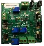
Figure 4 shows the top assembly view of the EVM. Figure 5 shows the top etch layer of the EVM, and
Figure 6 shows the bottom etch layer.
Figure 4. Top Assembly View
Figure 5. Board Layout – Top Etch Layer
8
bq24230H and bq24232H 0.5-A Single-Chip Li-Ion
Copyright © 2014, Texas Instruments Incorporated
SLVUA18 – January 2014
Submit Documentation Feedback
�Physical Layouts
www.ti.com
Figure 6. Board Layout – Bottom Etch Layer
SLVUA18 – January 2014
Submit Documentation Feedback
bq24230H and bq24232H 0.5-A Single-Chip Li-Ion
Copyright © 2014, Texas Instruments Incorporated
9
�Bill of Materials
5
www.ti.com
Bill of Materials
Designator
Quantity
Value
Description
Package
Reference
Printed Circuit Board
Part Number
Manufacturer
!PCB
1
PWR608
Any
C1, C4
2
10uF
CAP CER 10UF 25V 20% X5R 1206
1206
C3216X5R1E106M085AC
TDK
C2, C3
2
10uF
Capacitor, Ceramic, 10-uF, 6.3-V,
X5R, 20%
0805
GRM21BR60J106ME19K
Murata
D1
1
Red
Diode, LED, Red, 1.8-V, 10-mA, 10mcd
0603
160-1181-1-ND
Liteon
D2
1
Green
Diode, LED, Green, 2.1-V, 20-mA, 6mcd
0603
160-1183-1-ND
Liteon
BZX84C6V2-7-F
Diodes
D3
1
BZX84C6v2T
Diode, Zener, 6.2-V, 350-mW
SOT-23
J1, J2, J3, J4
4
ED555/2DS
Terminal Block, 2-pin, 6-A, 3.5mm
0.27 x 0.25 ED1514
OST
JP1, JP2, JP3, JP4, JP5
5
PEC03SAAN
Header, 3-pin, 100mil spacing
0.100 x 3
PEC03SAAN
Sullins
JP6, JP7
2
PEC02SAAN
Header, 2-pin, 100mil spacing
0.100 inch
x2
PEC02SAAN
Sullins
LBL1
1
Thermal Transfer Printable Labels,
0.650" W x 0.200" H - 10,000 per roll
PCB Label
0.650"H x
0.200"W
THT-14-423-10
Brady
P14, VSS
2
Void
None
R4
1
49.9k
Resistor, Chip, 1/10W, 1%
0603
CRCW060349K9FKEA
Vishay Dale
R5, R6, R21
3
1.5K
Resistor, Chip, 1/10W, 1%
0603
CRCW06031K50FKEA
Vishay Dale
R7, R19
2
0
Resistor, Chip, 1/10W, 1%
0603
CRCW06030000Z0EA
Vishay Dale
R8
1
5K
Potentiometer, 1/4 in. Cermet, 12Turn, Top-Adjust
0.25x0.17
inch
3266W-1-502LF
Bourns
R10, R11
2
10k
Potentiometer, 1/4 in. Cermet, 12Turn, Top-Adjust
0.25x0.17
3266W-1-103LF
Bourns
R12, R13, R15
3
10k
Resistor, Chip, 1/10W, 1%
0603
CRCW060310K0FKEA
Vishay Dale
R14
1
301k
Resistor, Chip, 1/10W, 1%
0603
CRCW0603301KFKEA
Vishay Dale
R16
1
50k
Potentiometer, 1/4 in. Cermet, 12Turn, Top-Adjust
0.25x0.17
3266W-1-503LF
Bourns
Test Point, O.032 Hole
R17
1
1k
Resistor, Chip, 1/10W, 1%
0603
CRCW06031K00FKEA
Vishay Dale
R18, R20
2
604
Resistor, Chip, 1/10W, 1%
0603
CRCW0603604RFKEA
Vishay Dale
SH-JP1, SH-JP2, SH-JP3,
SH-JP4, SH-JP5, SH-JP6,
SH-JP7
7
1x2
Shunt, 100mil, Gold plated, Black
Shunt
969102-0000-DA
3M
U1
1
QFN-16
BQ24232HRGE
TI
10
BQ24232HRG IC, USB- Friendly LiIon Battery
E
Charger and Power-Path
Managenment
bq24230H and bq24232H 0.5-A Single-Chip Li-Ion
Alternate Part
Number
Alternate
Manufacturer
-
-
-
-
SNT-100-BK-G
Samtec
None
SLVUA18 – January 2014
Submit Documentation Feedback
Copyright © 2014, Texas Instruments Incorporated
�Bill of Materials
www.ti.com
Designator
Quantity
Value
Description
Package
Reference
Part Number
FID1, FID2, FID3
0
Fiducial mark. There is nothing to buy Fiducial
or mount.
N/A
N/A
G4, G5, G6, G14, G15,
G16, HI4, HI5, HI6, HI15,
TP1, TP2, TP4, TP5, TP6,
TP10, TP12, TP13, TP14,
TP15, TP16
0
Test Point, O.032 Hole
Void
None
R1
0
732
Resistor, Chip, 1/10W, 1%
0603
CRCW0603732RFKEA
Vishay Dale
R2
0
1k
Resistor, Chip, 1/10W, 1%
0603
CRCW06031K00FKEA
Vishay Dale
R3, R9
0
10k
Resistor, Chip, 1/10W, 1%
0603
CRCW060310K0FKEA
Vishay Dale
R22
0
23.7k
Resistor, Chip, 1/10W, 1%
0603
CRCW060323K7FKEA
Vishay Dale
R23
0
11k
Resistor, Chip, 1/10W, 1%
0603
CRCW060311K0FKEA
Vishay Dale
SLVUA18 – January 2014
Submit Documentation Feedback
Manufacturer
Alternate Part
Number
Alternate
Manufacturer
bq24230H and bq24232H 0.5-A Single-Chip Li-Ion
Copyright © 2014, Texas Instruments Incorporated
11
�EVALUATION BOARD/KIT/MODULE (EVM) ADDITIONAL TERMS
Texas Instruments (TI) provides the enclosed Evaluation Board/Kit/Module (EVM) under the following conditions:
The user assumes all responsibility and liability for proper and safe handling of the goods. Further, the user indemnifies TI from all claims
arising from the handling or use of the goods.
Should this evaluation board/kit not meet the specifications indicated in the User’s Guide, the board/kit may be returned within 30 days from
the date of delivery for a full refund. THE FOREGOING LIMITED WARRANTY IS THE EXCLUSIVE WARRANTY MADE BY SELLER TO
BUYER AND IS IN LIEU OF ALL OTHER WARRANTIES, EXPRESSED, IMPLIED, OR STATUTORY, INCLUDING ANY WARRANTY OF
MERCHANTABILITY OR FITNESS FOR ANY PARTICULAR PURPOSE. EXCEPT TO THE EXTENT OF THE INDEMNITY SET FORTH
ABOVE, NEITHER PARTY SHALL BE LIABLE TO THE OTHER FOR ANY INDIRECT, SPECIAL, INCIDENTAL, OR CONSEQUENTIAL
DAMAGES.
Please read the User's Guide and, specifically, the Warnings and Restrictions notice in the User's Guide prior to handling the product. This
notice contains important safety information about temperatures and voltages. For additional information on TI's environmental and/or safety
programs, please visit www.ti.com/esh or contact TI.
No license is granted under any patent right or other intellectual property right of TI covering or relating to any machine, process, or
combination in which such TI products or services might be or are used. TI currently deals with a variety of customers for products, and
therefore our arrangement with the user is not exclusive. TI assumes no liability for applications assistance, customer product design,
software performance, or infringement of patents or services described herein.
REGULATORY COMPLIANCE INFORMATION
As noted in the EVM User’s Guide and/or EVM itself, this EVM and/or accompanying hardware may or may not be subject to the Federal
Communications Commission (FCC) and Industry Canada (IC) rules.
For EVMs not subject to the above rules, this evaluation board/kit/module is intended for use for ENGINEERING DEVELOPMENT,
DEMONSTRATION OR EVALUATION PURPOSES ONLY and is not considered by TI to be a finished end product fit for general consumer
use. It generates, uses, and can radiate radio frequency energy and has not been tested for compliance with the limits of computing
devices pursuant to part 15 of FCC or ICES-003 rules, which are designed to provide reasonable protection against radio frequency
interference. Operation of the equipment may cause interference with radio communications, in which case the user at his own expense will
be required to take whatever measures may be required to correct this interference.
General Statement for EVMs including a radio
User Power/Frequency Use Obligations: This radio is intended for development/professional use only in legally allocated frequency and
power limits. Any use of radio frequencies and/or power availability of this EVM and its development application(s) must comply with local
laws governing radio spectrum allocation and power limits for this evaluation module. It is the user’s sole responsibility to only operate this
radio in legally acceptable frequency space and within legally mandated power limitations. Any exceptions to this are strictly prohibited and
unauthorized by Texas Instruments unless user has obtained appropriate experimental/development licenses from local regulatory
authorities, which is responsibility of user including its acceptable authorization.
For EVMs annotated as FCC – FEDERAL COMMUNICATIONS COMMISSION Part 15 Compliant
Caution
This device complies with part 15 of the FCC Rules. Operation is subject to the following two conditions: (1) This device may not cause
harmful interference, and (2) this device must accept any interference received, including interference that may cause undesired operation.
Changes or modifications not expressly approved by the party responsible for compliance could void the user's authority to operate the
equipment.
FCC Interference Statement for Class A EVM devices
This equipment has been tested and found to comply with the limits for a Class A digital device, pursuant to part 15 of the FCC Rules.
These limits are designed to provide reasonable protection against harmful interference when the equipment is operated in a commercial
environment. This equipment generates, uses, and can radiate radio frequency energy and, if not installed and used in accordance with the
instruction manual, may cause harmful interference to radio communications. Operation of this equipment in a residential area is likely to
cause harmful interference in which case the user will be required to correct the interference at his own expense.
�FCC Interference Statement for Class B EVM devices
This equipment has been tested and found to comply with the limits for a Class B digital device, pursuant to part 15 of the FCC Rules.
These limits are designed to provide reasonable protection against harmful interference in a residential installation. This equipment
generates, uses and can radiate radio frequency energy and, if not installed and used in accordance with the instructions, may cause
harmful interference to radio communications. However, there is no guarantee that interference will not occur in a particular installation. If
this equipment does cause harmful interference to radio or television reception, which can be determined by turning the equipment off and
on, the user is encouraged to try to correct the interference by one or more of the following measures:
• Reorient or relocate the receiving antenna.
• Increase the separation between the equipment and receiver.
• Connect the equipment into an outlet on a circuit different from that to which the receiver is connected.
• Consult the dealer or an experienced radio/TV technician for help.
For EVMs annotated as IC – INDUSTRY CANADA Compliant
This Class A or B digital apparatus complies with Canadian ICES-003.
Changes or modifications not expressly approved by the party responsible for compliance could void the user’s authority to operate the
equipment.
Concerning EVMs including radio transmitters
This device complies with Industry Canada licence-exempt RSS standard(s). Operation is subject to the following two conditions: (1) this
device may not cause interference, and (2) this device must accept any interference, including interference that may cause undesired
operation of the device.
Concerning EVMs including detachable antennas
Under Industry Canada regulations, this radio transmitter may only operate using an antenna of a type and maximum (or lesser) gain
approved for the transmitter by Industry Canada. To reduce potential radio interference to other users, the antenna type and its gain should
be so chosen that the equivalent isotropically radiated power (e.i.r.p.) is not more than that necessary for successful communication.
This radio transmitter has been approved by Industry Canada to operate with the antenna types listed in the user guide with the maximum
permissible gain and required antenna impedance for each antenna type indicated. Antenna types not included in this list, having a gain
greater than the maximum gain indicated for that type, are strictly prohibited for use with this device.
Cet appareil numérique de la classe A ou B est conforme à la norme NMB-003 du Canada.
Les changements ou les modifications pas expressément approuvés par la partie responsable de la conformité ont pu vider l’autorité de
l'utilisateur pour actionner l'équipement.
Concernant les EVMs avec appareils radio
Le présent appareil est conforme aux CNR d'Industrie Canada applicables aux appareils radio exempts de licence. L'exploitation est
autorisée aux deux conditions suivantes : (1) l'appareil ne doit pas produire de brouillage, et (2) l'utilisateur de l'appareil doit accepter tout
brouillage radioélectrique subi, même si le brouillage est susceptible d'en compromettre le fonctionnement.
Concernant les EVMs avec antennes détachables
Conformément à la réglementation d'Industrie Canada, le présent émetteur radio peut fonctionner avec une antenne d'un type et d'un gain
maximal (ou inférieur) approuvé pour l'émetteur par Industrie Canada. Dans le but de réduire les risques de brouillage radioélectrique à
l'intention des autres utilisateurs, il faut choisir le type d'antenne et son gain de sorte que la puissance isotrope rayonnée équivalente
(p.i.r.e.) ne dépasse pas l'intensité nécessaire à l'établissement d'une communication satisfaisante.
Le présent émetteur radio a été approuvé par Industrie Canada pour fonctionner avec les types d'antenne énumérés dans le manuel
d’usage et ayant un gain admissible maximal et l'impédance requise pour chaque type d'antenne. Les types d'antenne non inclus dans
cette liste, ou dont le gain est supérieur au gain maximal indiqué, sont strictement interdits pour l'exploitation de l'émetteur.
SPACER
SPACER
SPACER
SPACER
SPACER
SPACER
SPACER
SPACER
�【Important Notice for Users of EVMs for RF Products in Japan】
】
This development kit is NOT certified as Confirming to Technical Regulations of Radio Law of Japan
If you use this product in Japan, you are required by Radio Law of Japan to follow the instructions below with respect to this product:
1.
2.
3.
Use this product in a shielded room or any other test facility as defined in the notification #173 issued by Ministry of Internal Affairs and
Communications on March 28, 2006, based on Sub-section 1.1 of Article 6 of the Ministry’s Rule for Enforcement of Radio Law of
Japan,
Use this product only after you obtained the license of Test Radio Station as provided in Radio Law of Japan with respect to this
product, or
Use of this product only after you obtained the Technical Regulations Conformity Certification as provided in Radio Law of Japan with
respect to this product. Also, please do not transfer this product, unless you give the same notice above to the transferee. Please note
that if you could not follow the instructions above, you will be subject to penalties of Radio Law of Japan.
Texas Instruments Japan Limited
(address) 24-1, Nishi-Shinjuku 6 chome, Shinjuku-ku, Tokyo, Japan
http://www.tij.co.jp
【無線電波を送信する製品の開発キットをお使いになる際の注意事項】
本開発キットは技術基準適合証明を受けておりません。
本製品のご使用に際しては、電波法遵守のため、以下のいずれかの措置を取っていただく必要がありますのでご注意ください。
1.
2.
3.
電波法施行規則第6条第1項第1号に基づく平成18年3月28日総務省告示第173号で定められた電波暗室等の試験設備でご使用いただく。
実験局の免許を取得後ご使用いただく。
技術基準適合証明を取得後ご使用いただく。
なお、本製品は、上記の「ご使用にあたっての注意」を譲渡先、移転先に通知しない限り、譲渡、移転できないものとします。
上記を遵守頂けない場合は、電波法の罰則が適用される可能性があることをご留意ください。
日本テキサス・インスツルメンツ株式会社
東京都新宿区西新宿6丁目24番1号
西新宿三井ビル
http://www.tij.co.jp
SPACER
SPACER
SPACER
SPACER
SPACER
SPACER
SPACER
SPACER
SPACER
SPACER
SPACER
SPACER
SPACER
SPACER
SPACER
SPACER
SPACER
�EVALUATION BOARD/KIT/MODULE (EVM)
WARNINGS, RESTRICTIONS AND DISCLAIMERS
For Feasibility Evaluation Only, in Laboratory/Development Environments. Unless otherwise indicated, this EVM is not a finished
electrical equipment and not intended for consumer use. It is intended solely for use for preliminary feasibility evaluation in
laboratory/development environments by technically qualified electronics experts who are familiar with the dangers and application risks
associated with handling electrical mechanical components, systems and subsystems. It should not be used as all or part of a finished end
product.
Your Sole Responsibility and Risk. You acknowledge, represent and agree that:
1.
2.
3.
4.
You have unique knowledge concerning Federal, State and local regulatory requirements (including but not limited to Food and Drug
Administration regulations, if applicable) which relate to your products and which relate to your use (and/or that of your employees,
affiliates, contractors or designees) of the EVM for evaluation, testing and other purposes.
You have full and exclusive responsibility to assure the safety and compliance of your products with all such laws and other applicable
regulatory requirements, and also to assure the safety of any activities to be conducted by you and/or your employees, affiliates,
contractors or designees, using the EVM. Further, you are responsible to assure that any interfaces (electronic and/or mechanical)
between the EVM and any human body are designed with suitable isolation and means to safely limit accessible leakage currents to
minimize the risk of electrical shock hazard.
Since the EVM is not a completed product, it may not meet all applicable regulatory and safety compliance standards (such as UL,
CSA, VDE, CE, RoHS and WEEE) which may normally be associated with similar items. You assume full responsibility to determine
and/or assure compliance with any such standards and related certifications as may be applicable. You will employ reasonable
safeguards to ensure that your use of the EVM will not result in any property damage, injury or death, even if the EVM should fail to
perform as described or expected.
You will take care of proper disposal and recycling of the EVM’s electronic components and packing materials.
Certain Instructions. It is important to operate this EVM within TI’s recommended specifications and environmental considerations per the
user guidelines. Exceeding the specified EVM ratings (including but not limited to input and output voltage, current, power, and
environmental ranges) may cause property damage, personal injury or death. If there are questions concerning these ratings please contact
a TI field representative prior to connecting interface electronics including input power and intended loads. Any loads applied outside of the
specified output range may result in unintended and/or inaccurate operation and/or possible permanent damage to the EVM and/or
interface electronics. Please consult the EVM User's Guide prior to connecting any load to the EVM output. If there is uncertainty as to the
load specification, please contact a TI field representative. During normal operation, some circuit components may have case temperatures
greater than 60°C as long as the input and output are maintained at a normal ambient operating temperature. These components include
but are not limited to linear regulators, switching transistors, pass transistors, and current sense resistors which can be identified using the
EVM schematic located in the EVM User's Guide. When placing measurement probes near these devices during normal operation, please
be aware that these devices may be very warm to the touch. As with all electronic evaluation tools, only qualified personnel knowledgeable
in electronic measurement and diagnostics normally found in development environments should use these EVMs.
Agreement to Defend, Indemnify and Hold Harmless. You agree to defend, indemnify and hold TI, its licensors and their representatives
harmless from and against any and all claims, damages, losses, expenses, costs and liabilities (collectively, "Claims") arising out of or in
connection with any use of the EVM that is not in accordance with the terms of the agreement. This obligation shall apply whether Claims
arise under law of tort or contract or any other legal theory, and even if the EVM fails to perform as described or expected.
Safety-Critical or Life-Critical Applications. If you intend to evaluate the components for possible use in safety critical applications (such
as life support) where a failure of the TI product would reasonably be expected to cause severe personal injury or death, such as devices
which are classified as FDA Class III or similar classification, then you must specifically notify TI of such intent and enter into a separate
Assurance and Indemnity Agreement.
Mailing Address: Texas Instruments, Post Office Box 655303, Dallas, Texas 75265
Copyright © 2014, Texas Instruments Incorporated
�IMPORTANT NOTICE
Texas Instruments Incorporated and its subsidiaries (TI) reserve the right to make corrections, enhancements, improvements and other
changes to its semiconductor products and services per JESD46, latest issue, and to discontinue any product or service per JESD48, latest
issue. Buyers should obtain the latest relevant information before placing orders and should verify that such information is current and
complete. All semiconductor products (also referred to herein as “components”) are sold subject to TI’s terms and conditions of sale
supplied at the time of order acknowledgment.
TI warrants performance of its components to the specifications applicable at the time of sale, in accordance with the warranty in TI’s terms
and conditions of sale of semiconductor products. Testing and other quality control techniques are used to the extent TI deems necessary
to support this warranty. Except where mandated by applicable law, testing of all parameters of each component is not necessarily
performed.
TI assumes no liability for applications assistance or the design of Buyers’ products. Buyers are responsible for their products and
applications using TI components. To minimize the risks associated with Buyers’ products and applications, Buyers should provide
adequate design and operating safeguards.
TI does not warrant or represent that any license, either express or implied, is granted under any patent right, copyright, mask work right, or
other intellectual property right relating to any combination, machine, or process in which TI components or services are used. Information
published by TI regarding third-party products or services does not constitute a license to use such products or services or a warranty or
endorsement thereof. Use of such information may require a license from a third party under the patents or other intellectual property of the
third party, or a license from TI under the patents or other intellectual property of TI.
Reproduction of significant portions of TI information in TI data books or data sheets is permissible only if reproduction is without alteration
and is accompanied by all associated warranties, conditions, limitations, and notices. TI is not responsible or liable for such altered
documentation. Information of third parties may be subject to additional restrictions.
Resale of TI components or services with statements different from or beyond the parameters stated by TI for that component or service
voids all express and any implied warranties for the associated TI component or service and is an unfair and deceptive business practice.
TI is not responsible or liable for any such statements.
Buyer acknowledges and agrees that it is solely responsible for compliance with all legal, regulatory and safety-related requirements
concerning its products, and any use of TI components in its applications, notwithstanding any applications-related information or support
that may be provided by TI. Buyer represents and agrees that it has all the necessary expertise to create and implement safeguards which
anticipate dangerous consequences of failures, monitor failures and their consequences, lessen the likelihood of failures that might cause
harm and take appropriate remedial actions. Buyer will fully indemnify TI and its representatives against any damages arising out of the use
of any TI components in safety-critical applications.
In some cases, TI components may be promoted specifically to facilitate safety-related applications. With such components, TI’s goal is to
help enable customers to design and create their own end-product solutions that meet applicable functional safety standards and
requirements. Nonetheless, such components are subject to these terms.
No TI components are authorized for use in FDA Class III (or similar life-critical medical equipment) unless authorized officers of the parties
have executed a special agreement specifically governing such use.
Only those TI components which TI has specifically designated as military grade or “enhanced plastic” are designed and intended for use in
military/aerospace applications or environments. Buyer acknowledges and agrees that any military or aerospace use of TI components
which have not been so designated is solely at the Buyer's risk, and that Buyer is solely responsible for compliance with all legal and
regulatory requirements in connection with such use.
TI has specifically designated certain components as meeting ISO/TS16949 requirements, mainly for automotive use. In any case of use of
non-designated products, TI will not be responsible for any failure to meet ISO/TS16949.
Products
Applications
Audio
www.ti.com/audio
Automotive and Transportation
www.ti.com/automotive
Amplifiers
amplifier.ti.com
Communications and Telecom
www.ti.com/communications
Data Converters
dataconverter.ti.com
Computers and Peripherals
www.ti.com/computers
DLP® Products
www.dlp.com
Consumer Electronics
www.ti.com/consumer-apps
DSP
dsp.ti.com
Energy and Lighting
www.ti.com/energy
Clocks and Timers
www.ti.com/clocks
Industrial
www.ti.com/industrial
Interface
interface.ti.com
Medical
www.ti.com/medical
Logic
logic.ti.com
Security
www.ti.com/security
Power Mgmt
power.ti.com
Space, Avionics and Defense
www.ti.com/space-avionics-defense
Microcontrollers
microcontroller.ti.com
Video and Imaging
www.ti.com/video
RFID
www.ti-rfid.com
OMAP Applications Processors
www.ti.com/omap
TI E2E Community
e2e.ti.com
Wireless Connectivity
www.ti.com/wirelessconnectivity
Mailing Address: Texas Instruments, Post Office Box 655303, Dallas, Texas 75265
Copyright © 2014, Texas Instruments Incorporated
�


 工商网监
湘ICP备2023018690号
工商网监
湘ICP备2023018690号
