bq24750A
www.ti.com .......................................................................................................................................................... SLUS834A – JULY 2008 – REVISED MARCH 2009
Host-Controlled Multi-Chemistry Battery Charger with Low Iq and Integrated System
Power Selector
•
PGND
LODRV
REGN
PH
28 27 26 25 24 23 22
CHGEN
1
21
DPMDET
ACN
2
20
CELLS
ACP
3
bq24750A
19
SRP
ACDRV
4
28 LD QFN
18
SRN
ACDET
5
TOP VIEW
17
BAT
ACSET
6
16
SRSET
ACOP
7
15
IADAPT
9
10 11 12 13 14
BATDRV
8
ACGOOD
•
The bq24750A is a high-efficiency, synchronous
battery charger with integrated compensation and
system power selector logic, offering low component
count for space-constrained multi-chemistry battery
charging applications. Ratiometric charge current and
voltage programming allows high regulation
accuracies, and can be either hardwired with resistors
or programmed by the system power-management
microcontroller using a DAC or GPIOs.
VADJ
•
DESCRIPTION
VDAC
•
•
•
Notebook and Ultra-Mobile Computers
Portable Data-Capture Terminals
Portable Printers
Medical Diagnostics Equipment
Battery Bay Chargers
Battery Back-up Systems
HIDRV
•
•
•
•
•
•
•
VREF
•
APPLICATIONS
BTST
•
PVCC
•
NMOS-NMOS Synchronous Buck Converter
with 300 kHz Frequency and >95% Efficiency
30-ns Minimum Driver Dead-time and 99.5%
Maximum Effective Duty Cycle
High-Accuracy Voltage and Current Regulation
– ±0.5% Charge Voltage Accuracy
– ±3% Charge Current Accuracy
– ±3% Adapter Current Accuracy
– ±2% Input Current Sense Amp Accuracy
Integration
– Automatic System Power Selection From
AC/DC Adapter or Battery
– Internal Loop Compensation
– Internal Soft Start
Safety
– Input Overvoltage Protection (OVP)
– Dynamic Power Management (DPM) with
Status Indicator
– Programmable Inrush Adapter Power
(ACOP) and Overcurrent (ACOC) Limits
– Reverse-Conduction Protection Input FET
– Battery Thermistor Sense Input (TS) for
Charge Qualification
Supports Two, Three, or Four Li+ Cells
5–24 V AC/DC-Adapter Operating Range
Analog Inputs with Ratiometric Programming
via Resistors or DAC/GPIO Host Control
– Charge Voltage (4–4.512 V/cell)
– Charge Current (up to 10 A, with 10 mΩ
sense resistor)
– Adapter Current Limit (DPM)
Status and Monitoring Outputs
– AC/DC Adapter Present with Programmable
Voltage Threshold
– DPM Loop Active
– Current Drawn from Input Source
Supports Any Battery Chemistry: Li+, NiCd,
NiMH, Lead Acid, etc.
Charge Enable
28-pin, 5x5-mm QFN package
Energy Star Low Iq
– < 10 µA Off-State Battery Discharge Current
– < 1.5 mA Off-State Input Qiescent Current
TS
•
•
•
AGND
FEATURES
1
1
Please be aware that an important notice concerning availability, standard warranty, and use in critical applications of Texas
Instruments semiconductor products and disclaimers thereto appears at the end of this data sheet.
PRODUCTION DATA information is current as of publication date.
Products conform to specifications per the terms of the Texas
Instruments standard warranty. Production processing does not
necessarily include testing of all parameters.
Copyright © 2008–2009, Texas Instruments Incorporated
�bq24750A
SLUS834A – JULY 2008 – REVISED MARCH 2009 .......................................................................................................................................................... www.ti.com
These devices have limited built-in ESD protection. The leads should be shorted together or the device placed in conductive foam
during storage or handling to prevent electrostatic damage to the MOS gates.
DESCRIPTION (CONTINUED)
The bq24750A charges two, three, or four series Li+ cells, supporting up to 10 A of charge current, and is
available in a 28-pin, 5x5-mm QFN package.
The bq24750A controls external switches to prevent battery discharge back to the input, connect the adapter to
the system, and to connect the battery to the system using 6-V gate drives for better system efficiency. For
maximum system safety, inrush-power limiting provides instantaneous response to high input voltage multiplied
by current. This AC Over-Power protection (ACOP) feature limits the input-switch power to the programmed level
on the ACOP pin, and latches off if the high-power condition persists to prevent overheating.
The bq24750A features Dynamic Power Management (DPM) and input power limiting. These features reduce
battery charge current when the input power limit is reached to avoid overloading the AC adapter when supplying
the load and the battery charger simultaneously. A highly-accurate current-sense amplifier enables precise
measurement of input current from the AC adapter to monitor the overall system power.
ADAPTER +
ADAPTER -
SYSTEM
R10
2Ω
C1
2.2 µF
R1
P
Q1 (ACFET)
SI4435
C6
10 µF
RAC
0.010 Ω
P
C7
10 µF
Q2 (ACFET)
SI4435
C3
C2
0.1 µF
432 kΩ
1%
0.1 µF
ACN
PVCC
C8
0.1 µF
ACP
/ACDRV
Q3(BATFET)
SI4435
/BATDRV
ACDET
66.5 kΩ
1%
VREF
/ACGOOD
AGND
VREF
R5
10 kΩ
R3
5.6 kΩ
1%
bq24750A
L1
8.2 µH
PH
REGN
R4
118 kΩ
1%
C9
0.1 µF
C10
1 µF
LODRV
N
C4
0.1 µF
SRN
CELLS
BAT
C15
0.1 µF
/CHGEN
ACOP
VDAC
C16
0.47 µF
DAC
VADJ
ADC
C14
0.1 µF
SRP
/DPMDET
GPIO
PACK-
PGND
VREF
R6
10 kΩ
C12
10 µF
C11
10 µF
C13
0.1 µF
Q5
FDS6680A
SRSET
ACSET
HOST
RSR
0.010 Ω
PACK+
D1
BAT54
TS
DAC
P
BTST
/ACGOOD
PACK
THERMISTER
SENSE
N
R2
Q4
FDS6680A
HIDRV
IADAPT
PowerPad
C5
100 pF
A.
VIN=20 V, VBAT = 3-cell Li-Ion, ICHARGE = 3 A, IADAPTER_LIMIT = 4 A, TBAT = 0-45°C
Figure 1. Typical System Schematic, Voltage and Current Programmed by DAC
2
Submit Documentation Feedback
Copyright © 2008–2009, Texas Instruments Incorporated
Product Folder Link(s) :bq24750A
�bq24750A
www.ti.com .......................................................................................................................................................... SLUS834A – JULY 2008 – REVISED MARCH 2009
ADAPTER +
SYSTEM
R10
2Ω
ADAPTER -
C1
2.2 µF
R1
P
P
Q1 (ACFET)
SI4435
C6
10 µF
RAC
0.010 Ω
C7
10 µF
Q2 (ACFET)
SI4435
C3
C2
0.1 µF
432 kΩ
1%
ACN
0.1 µF
PVCC
C8
0.1 µF
ACP
/ACDRV
Q3(BATFET)
SI4435
/BATDRV
ACDET
66.5 kΩ
1%
VREF
AGND
VREF
R5
10 kΩ
R3
5.6 kΩ
1%
N
R2
bq24750A
/ACGOOD
VREF
R4
118 kΩ
1%
R11
REGN
R7
100 kΩ
C9
0.1 µF
C10
1 µF
43 kΩ
C13
0.1 µF
Q5
FDS6680A
LODRV
ACSET
R9
66.5 kΩ
N
C4
0.1µF
R6
10 kΩ
PACK-
C14
0.1 µF
PGND
VREF
HOST
C12
10 µF
C11
10 µF
SRSET
R8
100 kΩ
RSR
0.010 Ω
PACK+
D1
BAT54
TS
VREF
L1
8.2 µH
PH
P
BTST
/ACGOOD
PACK
THERMISTER
SENSE
Q4
FDS6680A
HIDRV
SRP
/DPMDET
GPIO
SRN
CELLS
BAT
C15
0.1 µF
/CHGEN
VREF
ACOP
VDAC
C16
0.47 µF
REGN
VADJ
ADC
PowerPad
IADAPT
C5
100 pF
A.
VIN=20 V, VBAT = 3-cell Li-Ion, ICHARGE = 3 A, IADAPTER_LIMIT = 4 A, TBAT = 0-45°C
Figure 2. Typical System Schematic, Voltage and Current Programmed by Resistor
ORDERING INFORMATION
ORDERING NUMBER
(TAPE and REEL)
PART NUMBER
PACKAGE
bq24750A
28-PIN 5 x 5 mm QFN
QUANTITY
bq24750ARHDT
250
bq24750ARHDR
3000
PACKAGE THERMAL DATA
over operating free-air temperature range (unless otherwise noted)
(1)
(2)
PACKAGE
θJA
POWER RATING
TA = 70°C
DERATING FACTOR ABOVE
TA = 70 °C
QFN – RHD (1) (2)
39 °C/W
2.36 W
0.028 W/°C
For the most current package and ordering information, see the Package Option Addendum at the end of this document, or see the TI
Web site at www.ti.com.
This data is based on using the JEDEC High-K board and the exposed die pad is connected to a Cu pad on the board. This is
connected to the ground plane by a 2x3 via matrix.
Submit Documentation Feedback
Copyright © 2008–2009, Texas Instruments Incorporated
Product Folder Link(s) :bq24750A
3
�bq24750A
SLUS834A – JULY 2008 – REVISED MARCH 2009 .......................................................................................................................................................... www.ti.com
Table 1. TERMINAL FUNCTIONS – 28-PIN QFN
TERMINAL
NAME
NO.
DESCRIPTION
CHGEN
1
Charge enable active-low logic input. LO enables charge. HI disables charge.
ACN
2
Adapter current sense resistor, negative input. A 0.1-µF ceramic capacitor is placed from ACN to ACP to provide
differential-mode filtering. An optional 0.1-µF ceramic capacitor is placed from ACN pin to AGND for common-mode
filtering.
ACP
3
Adapter current sense resistor, positive input. A 0.1-µF ceramic capacitor is placed from ACN to ACP to provide
differential-mode filtering. A 0.1-µF ceramic capacitor is placed from ACP pin to AGND for common-mode filtering.
ACDRV
4
AC adapter to system-switch driver output. Connect directly to the gate of the ACFET P-channel power MOSFET and
the reverse conduction blocking P-channel power MOSFET. Connect both FETs as common-source. Connect the
ACFET drain to the system-load side. The PVCC should be connected to the common-source node to ensure that the
driver logic is always active when needed. If needed, an optional capacitor from gate to source of the ACFET is used
to slow down the ON and OFF times. The internal gate drive is asymmetrical, allowing a quick turn-off and slower
turn-on in addition to the internal break-before-make logic with respect to the BATDRV. The output goes into linear
regulation mode when the input sensed current exceeds the ACOC threshold. ACDRV is latched off after ACOP
voltage exceeds 2 V, to protect the charging system from an ACFET-overpower condition.
ACDET
5
Adapter detected voltage set input. Program the adapter detect threshold by connecting a resistor divider from adapter
input to ACDET pin to AGND pin. Adapter voltage is detected if ACDET-pin voltage is greater than 2.4 V. The IADAPT
current sense amplifier is active when the ACDET pin voltage is greater than 0.6 V. Input overvoltage, ACOV, disables
charge and ACDRV when ACDET > 3.1 V. ACOV does not latch.
ACSET
6
Adapter current set input. The voltage ratio of ACSET voltage versus VDAC voltage programs the input current
regulation set-point during Dynamic Power Management (DPM). Program by connecting a resistor divider from VDAC
to ACSET to AGND; or by connecting the output of an external DAC to the ACSET pin and connect the DAC supply to
the VDAC pin.
ACOP
7
Input power limit set input. Program the input over-power time constant by placing a ceramic capacitor from ACOP to
AGND. The capacitor sets the time that the input current limit, ACOC, can be sustained before exceeding the
power-MOSFET power limit. When the ACOP voltage exceeds 2 V, then the ACDRV latches off to protect the charge
system from an over-power condition, ACOP. Reset latch by toggling ACDET or PVCC_UVLO.
TS
8
Temperature qualification voltage input for battery pack negative temperature coefficient thermistor. Program the hot
and cold temperature window with a resistor divider from VREF to TS to AGND.
AGND
9
Analog ground. Ground connection for low-current sensitive analog and digital signals. On PCB layout, connect to the
analog ground plane, and only connect to PGND through the PowerPad underneath the IC.
VREF
10
3.3-V regulated voltage output. Place a 0.1-µF ceramic capacitor from VREF to AGND pin close to the IC. This voltage
could be used for ratiometric programming of voltage and current regulation. Do not apply a external voltage source to
this pin.
VDAC
11
Charge voltage set reference input. Connect the VREF or external DAC voltage source to the VDAC pin. Battery
voltage, charge current, and input current are programmed as a ratio of the VDAC pin voltage versus the VADJ,
SRSET, and ACSET pin voltages, respectively. Place resistor dividers from VDAC to VADJ, SRSET, and ACSET pins
to AGND for programming. A DAC could be used by connecting the DAC supply to VDAC and connecting the output
to VADJ, SRSET, or ACSET.
VADJ
12
Charge voltage set input. The voltage ratio of VADJ voltage versus VDAC voltage programs the battery voltage
regulation set-point. Program by connecting a resistor divider from VDAC to VADJ, to AGND; or, by connecting the
output of an external DAC to VADJ, and connect the DAC supply to VDAC. VADJ connected to REGN programs the
default of 4.2 V per cell.
ACGOOD
13
Valid adapter active-low detect logic open-drain output. Pulled low when Input voltage is above programmed ACDET.
Connect a 10-kΩ pullup resistor from ACGOOD to VREF, or to a different pullup-supply rail.
BATDRV
14
Battery to system switch driver output. Gate drive for the battery to system load BAT PMOS power FET to isolate the
system from the battery to prevent current flow from the system to the battery, while allowing a low impedance path
from battery to system and while discharging the battery pack to the system load. Connect this pin directly to the gate
of the input BAT P-channel power MOSFET. Connect the source of the FET to the system load voltage node. Connect
the drain of the FET to the battery pack positive node. An optional capacitor is placed from the gate to the source to
slow-down the switching times. The internal gate drive is asymmetrical to allow a quick turn-off and slower turn-on, in
addition to the internal break-before-make logic with respect to the ACDRV.
IADAPT
15
Adapter current sense amplifier output. IADAPT voltage is 20 times the differential voltage across ACP-ACN. Place a
100-pF or less ceramic decoupling capacitor from IADAPT to AGND.
SRSET
16
Charge current set input. The voltage ratio of SRSET voltage versus VDAC voltage programs the charge current
regulation set-point. Program by connecting a resistor divider from VDAC to SRSET to AGND; or by connecting the
output of an external DAC to SRSET pin and connect the DAC supply to VDAC pin.
BAT
17
Battery voltage remote sense. Directly connect a kelvin sense trace from the battery pack positive terminal to the BAT
pin to accurately sense the battery pack voltage. Place a 0.1-µF capacitor from BAT to AGND close to the IC to filter
high-frequency noise.
4
Submit Documentation Feedback
Copyright © 2008–2009, Texas Instruments Incorporated
Product Folder Link(s) :bq24750A
�bq24750A
www.ti.com .......................................................................................................................................................... SLUS834A – JULY 2008 – REVISED MARCH 2009
Table 1. TERMINAL FUNCTIONS – 28-PIN QFN (continued)
TERMINAL
NAME
NO.
DESCRIPTION
SRN
18
Charge current sense resistor, negative input. A 0.1-µF ceramic capacitor is placed from SRN to SRP to provide
differential-mode filtering. An optional 0.1-µF ceramic capacitor is placed from SRN pin to AGND for common-mode
filtering.
SRP
19
Charge current sense resistor, positive input. A 0.1-µF ceramic capacitor is placed from SRN to SRP to provide
differential-mode filtering. A 0.1-µF ceramic capacitor is placed from SRP pin to AGND for common-mode filtering.
CELLS
20
2, 3 or 4 cells selection logic input. Logic low programs 3 cell. Logic high programs 4 cell. Floating programs 2 cell.
DPMDET
21
Dynamic power management (DPM) input current loop active, open-drain output status. Logic low indicates input
current is being limited by reducing the charge current. Connect 10-kΩ pullup resistor from DPMDET to VREF or a
different pullup-supply rail. Time delay is 10 ms.
PGND
22
Power ground. Ground connection for high-current power converter node. On PCB layout, connect directly to source of
low-side power MOSFET, to ground connection of in put and output capacitors of the charger. Only connect to AGND
through the PowerPad underneath the IC.
LODRV
23
PWM low side driver output. Connect to the gate of the low-side power MOSFET with a short trace.
REGN
24
PWM low side driver positive 6-V supply output. Connect a 1-µF ceramic capacitor from REGN to PGND, close to the
IC. Use for high-side driver bootstrap voltage by connecting a small-signal Schottky diode from REGN to BTST. REGN
is disabled when CHGEN is high.
PH
25
PWM high side driver negative supply. Connect to the phase switching node (junction of the low-side power MOSFET
drain, high-side power MOSFET source, and output inductor). Connect the 0.1-µF bootstrap capacitor from from PH to
BTST.
HIDRV
26
PWM high side driver output. Connect to the gate of the high-side power MOSFET with a short trace.
BTST
27
PWM high side driver positive supply. Connect a 0.1-µF bootstrap ceramic capacitor from BTST to PH. Connect a
small bootstrap Schottky diode from REGN to BTST.
PVCC
28
IC power positive supply. Connect to the common-source (diode-OR) point: source of high-side P-channel MOSFET
and source of reverse-blocking power P-channel MOSFET. Place a 0.1-µF ceramic capacitor from PVCC to PGND pin
close to the IC.
PowerPad
Exposed pad beneath the IC. AGND and PGND star-connected only at the PowerPad plane. Always solder PowerPad
to the board, and have vias on the PowerPad plane connecting to AGND and PGND planes. It also serves as a
thermal pad to dissipate the heat.
ABSOLUTE MAXIMUM RATINGS
over operating free-air temperature range (unless otherwise noted) (1)
(2)
VALUE
PVCC, ACP, ACN, SRP, SRN, BAT, BATDRV, ACDRV
Voltage range
Maximum difference voltage
–0.3 to 30
PH
–1 to 30
REGN, LODRV, VADJ, ACSET, SRSET, TS, ACDET, ACOP, CHGEN, CELLS,
ACGOOD
–0.3 to 7
V
VDAC
–0.3 to 5.5
VREF, IADAPT
–0.3 to 3.6
BTST, HIDRV with respect to AGND and PGND
–0.3 to 36
ACP–ACN, SRP–SRN, AGND–PGND
–0.5 to 0.5
Junction temperature range
–40 to 155
Storage temperature range
–55 to 155
(1)
(2)
UNIT
V
°C
Stresses beyond those listed under absolute maximum ratings may cause permanent damage to the device. These are stress ratings
only, and functional operation of the device at these or any other conditions beyond those indicated under recommended operating
conditions is not implied. Exposure to absolute-maximum-rated conditions for extended periods may affect device reliability.
All voltages are with respect to GND if not specified. Currents are positive into, negative out of the specified terminal. Consult Packaging
Section of the data book for thermal limitations and considerations of packages.
Submit Documentation Feedback
Copyright © 2008–2009, Texas Instruments Incorporated
Product Folder Link(s) :bq24750A
5
�bq24750A
SLUS834A – JULY 2008 – REVISED MARCH 2009 .......................................................................................................................................................... www.ti.com
RECOMMENDED OPERATING CONDITIONS
over operating free-air temperature range (unless otherwise noted)
MIN
PH
Voltage range
NOM
MAX
–1
24
PVCC, ACP, ACN, SRP, SRN, BAT, BATDRV, ACDRV
0
24
REGN, LODRV
0
6.5
VDAC, IADAPT
0
VREF
UNIT
3.6
3.3
V
ACSET, SRSET, TS, ACDET, ACOP, CHGEN, CELLS, ACGOOD, DPMDET
0
5.5
VADJ
0
6.5
BTST, HIDRV with respect to AGND and PGND
0
30
0.3
AGND, PGND
–0.3
Maximum difference voltage: ACP–ACN, SRP–SRN
–0.3
0.3
Junction temperature range, TJ
–40
125
Storage temperature range, Tstg
–55
150
V
°C
ELECTRICAL CHARACTERISTICS
7 V ≤ VPVCC ≤ 24 V, 0°C < TJ < +125°C, typical values are at TA = 25°C, with respect to AGND (unless otherwise noted)
PARAMETER
TEST CONDITIONS
MIN
TYP
MAX
UNIT
OPERATING CONDITIONS
VPVCC_OP
PVCC Input voltage operating range
5
24
V
8
18.048
V
CHARGE VOLTAGE REGULATION
VBAT_REG_RNG
BAT voltage regulation range
VVDAC_OP
VDAC reference voltage range
VADJ_OP
VADJ voltage range
4-4.512 V per cell, times 2,3,4 cells
Charge voltage regulation accuracy
Charge voltage regulation set to
default to 4.2 V per cell
2.6
3.6
V
0
REGN
V
8 V, 8.4 V, 9.024 V
–0.5%
0.5%
12 V, 12.6 V, 13.536 V
–0.5%
0.5%
16 V, 16.8 V, 18.048 V
–0.5%
0.5%
VADJ connected to REGN, 8.4 V, 12.6 V,
16.8 V
–0.5%
0.5%
0
100
CHARGE CURRENT REGULATION
VIREG_CHG
Charge current regulation differential
VIREG_CHG = VSRP – VSRN
voltage range
VSRSET_OP
SRSET voltage range
Charge current regulation accuracy
0
VDAC
VIREG_CHG = 40–100 mV
–3%
3%
VIREG_CHG = 20 mV
–5%
5%
VIREG_CHG = 5 mV
–25%
25%
VIREG_CHG = 1.5 mV (VBAT>4V)
–33%
33%
0
100
0
VDAC
–3%
3%
mV
V
INPUT CURRENT REGULATION
VIREG_DPM
Adapter current regulation
differential voltage range
VACSET_OP
ACSET voltage range
VIREG_DPM = VACP – VACN
VIREG_DPM = 40–100 mV
Input current regulation accuracy
VIREG_DPM = 20 mV
–5%
5%
VIREG_DPM = 5 mV
–25%
25%
VIREG_DPM = 1.5 mV
–33%
33%
3.267
mV
V
VREF REGULATOR
VVREF_REG
VREF regulator voltage
VACDET > 0.6 V, 0-30 mA
IVREF_LIM
VREF current limit
VVREF = 0 V, VACDET > 0.6 V
6
Submit Documentation Feedback
35
3.3
3.333
80
V
mA
Copyright © 2008–2009, Texas Instruments Incorporated
Product Folder Link(s) :bq24750A
�bq24750A
www.ti.com .......................................................................................................................................................... SLUS834A – JULY 2008 – REVISED MARCH 2009
ELECTRICAL CHARACTERISTICS (continued)
7 V ≤ VPVCC ≤ 24 V, 0°C < TJ < +125°C, typical values are at TA = 25°C, with respect to AGND (unless otherwise noted)
PARAMETER
TEST CONDITIONS
MIN
TYP
MAX
UNIT
5.9
6.2
V
mA
REGN REGULATOR
VREGN_REG
REGN regulator voltage
VACDET > 0.6 V, 0-75 mA, PVCC > 10 V
5.6
IREGN_LIM
REGN current limit
VREGN = 0 V, VACDET > 0.6 V
90
135
0
24
0
2
ADAPTER CURRENT SENSE AMPLIFIER
VACP/N_OP
Input common mode range
Voltage on ACP/ACN
VIADAPT
IADAPT output voltage range
IIADAPT
IADAPT output current
AIADAPT
Current sense amplifier voltage gain
0
Adapter current sense accuracy
AIADAPT = VIADAPT / VIREG_DPM
1
20
–2%
VIREG_DPM = 20 mV
–3%
3%
VIREG_DPM = 5 mV
–25%
25%
VIREG_DPM = 1.5 mV
–33%
33%
Output current limit
VIADAPT = 0 V
CIADAPT_MAX
Maximum output load capacitance
For stability with 0 mA to 1 mA load
mA
V/V
VIREG_DPM = 40–100 mV
IIADAPT_LIM
V
2%
1
mA
100
pF
2.424
V
ACDET COMPARATOR
VACDET_CHG
ACDET adapter-detect rising
threshold
Min voltage to enable charging, VACDET
rising
VACDET_CHG_HYS
ACDET falling hysteresis
VACDET falling
ACDET rising deglitch
2.376
2.40
VACDET rising
518
700
908
ms
ACDET falling deglitch
VACDET falling
7
9
11
ms
VACDET_BIAS
ACDET enable-bias rising threshold
Min voltage to enable all bias, VACDET
rising
0.56
0.62
0.68
VACDET_BIAS_HYS
Adapter present falling hysteresis
VACDET falling
20
mV
ACDET rising deglitch
VACDET rising
10
µs
ACDET falling deglitch
VACDET falling
10
µs
40
mV
V
PVCC / BAT COMPARATOR (REVERSE DISCHARGING PROTECTION)
VPVCC-BAT_OP
Differential Voltage from PVCC to
BAT
VPVCC-BAT_FALL
PVCC to BAT falling threshold
VPVCC-BAT_HYS
–20
VPVCC – VBAT to turn off ACFET
140
PVCC to BAT hysteresis
24
185
240
50
PVCC to BAT Rising Deglitch
VPVCC – VBAT > VPVCC-BAT_RISE
PVCC to BAT Falling Deglitch
VPVCC – VBAT < VPVCC-BAT_FALL
7
9
V
mV
mV
11
ms
µs
6
INPUT UNDERVOLTAGE LOCK-OUT COMPARATOR (UVLO)
UVLO
AC Undervoltage rising threshold
UVLO(HYS)
AC Undervoltage hysteresis, falling
Measured on PVCC
3.5
4
4.5
260
V
mV
AC LOW VOLTAGE COMPARATOR (ACLOWV)
VACLOWV
AC low voltage rising threshold
AC low voltage falling threshold
3.6
Measure on ACP pin
V
3
ACN / BAT COMPARATOR
VACN-BAT_FALL
ACN to BAT falling threshold
VACN-BAT_HYS
ACN to BAT hysteresis
VACN – VBAT to turn on BATDRV
175
285
340
mV
50
mV
ACN to BAT rising deglitch
VACN – VBAT > VACN-BAT_RISE
20
µs
ACN to BAT falling deglitch
VACN – VBAT < VACN-BAT_FALL
6
µs
BAT OVERVOLTAGE COMPARATOR
VOV_RISE
Overvoltage rising threshold
As percentage of VBAT_REG
104%
VOV_FALL
Overvoltage falling threshold
As percentage of VBAT_REG
102%
Submit Documentation Feedback
Copyright © 2008–2009, Texas Instruments Incorporated
Product Folder Link(s) :bq24750A
7
�bq24750A
SLUS834A – JULY 2008 – REVISED MARCH 2009 .......................................................................................................................................................... www.ti.com
ELECTRICAL CHARACTERISTICS (continued)
7 V ≤ VPVCC ≤ 24 V, 0°C < TJ < +125°C, typical values are at TA = 25°C, with respect to AGND (unless otherwise noted)
PARAMETER
TEST CONDITIONS
MIN
TYP
MAX
UNIT
CHARGE OVERCURRENT COMPARATOR
VOC
Charge overcurrent falling threshold
OCP Floor
OCP Threshold
As percentage of IREG_CHG
145%
50
mV
falling threshold
0.1xSRSET/VDAC falling
33.75
mV
rising threshold
0.1xSRSET/VDAC rising
42.5
mV
Minimum current Limit (SRP-SRN)
CHARGE UNDERCURRENT COMPARATOR (SYNCHRONOUS TO NON-SYNCHRONOUS TRANSITION)
VISYNSET_FALL
Charge undercurrent falling
threshold
VISYNSET_HYS
Charge undercurrent rising
hysteresis
Changing from synchronous to
non-sysnchronous
9.75
13
16.25
8
Charge undercurrent, falling-current
deglitch
Charge undercurrent, rising-current
deglitch
mV
mV
20
µs
VIREG_DPM < VISYNSET
640
INPUT OVER-POWER COMPARATOR (ACOP)
VACOC
ACOC Gain for initial ACOC current
limit (Percentage of programmed
VIREG_DPM)
Begins 700 ms after ACDET
Input current limited to this threshold for
fault protection
150
%
VIREG_DPM
VACOC_CEILING
Maximum ACOC input current limit
(VACP–VACN)max
Internally limited ceiling
VACOC_MAX = (VACP – VACN)max
100
mV
ACOP Latch Blankout Time with
ACOC active
(begins 700 ms after ACDET)
Begins 700 ms after ACDET
(does not allow ACOP latch-off, and no
ACOP source current)
2
ms
VACOP
ACOP pin latch-off threshold voltage
(See ACOP in Terminal Functions
table )
KACOP
Gain for ACOP Source Current
when in ACOC
Current source on when in ACOC limit.
Function of voltage across power FET
IACOP_SOURCE = KACOP × (VPVCC - VACP)
IACOP_SINK
ACOP Sink Current when not in
ACOC
ACOP Latch is reset by going below
ACDET or UVLO
Current sink on when not in ACOC
1.95
2
2.05
V
18
µA / V
5
µA
INPUT OVERVOLTAGE COMPARATOR (ACOV)
AC Over-voltage rising threshold on
ACDET
(See ACDET in Terminal Functions)
VACOV
VACOV_HYS
Measured on ACDET
3.007
3.1
AC Over-voltage rising deglitch
1.3
AC Over-voltage falling deglitch
1.3
3.193
V
ms
THERMAL SHUTDOWN COMPARATOR
TSHUT
Thermal shutdown rising
temperature
TSHUT_HYS
Thermal shutdown hysteresis, falling
Temperature Increasing
155
°C
20
°C
THERMISTER COMPARATOR (TS)
VLTF
Cold temperature rising threshold
As percentage to VVREF
72.5% 73.8% 74.2%
VLTF_HYS
Rising hysteresis
As percentage to VVREF
VTCO
Cut-off temperature rising threshold
As percentage to VVREF
28.7% 29.3% 29.9%
VHTF
Hot temperature rising threshold
As percentage to VVREF
33.7% 34.4% 35.1%
Deglitch time for temperature out of
range detection
VTS > VLTF, or VTS < VTCO, or
VTS < VHTF
0.5%
Submit Documentation Feedback
1.5%
10
Deglitch time for temperature in valid VTS > VLTF – VLTF_HYS or VTS > VTCO,
range detection
or VTS > VHTF
8
1%
ms
10
Copyright © 2008–2009, Texas Instruments Incorporated
Product Folder Link(s) :bq24750A
�bq24750A
www.ti.com .......................................................................................................................................................... SLUS834A – JULY 2008 – REVISED MARCH 2009
ELECTRICAL CHARACTERISTICS (continued)
7 V ≤ VPVCC ≤ 24 V, 0°C < TJ < +125°C, typical values are at TA = 25°C, with respect to AGND (unless otherwise noted)
PARAMETER
TEST CONDITIONS
MIN
TYP
MAX
UNIT
BATTERY SWITCH (BATDRV) DRIVER
RDS(off)_BAT
BATFET Turn-off resistance
VACN > 5 V
160
Ω
RDS(on)_BAT
BATFET Turn-on resistance
VACN > 5 V
3
kΩ
BATFET drive voltage
VBATDRV_REG = VACN – VBATDRV when
VACN > 5 V and BATFET is on
BATFET Power-up delay
Delay to turn off BATFET after adapter is
detected (after ACDET > 2.4)
V/BATDRV_REG
6.5
518
700
V
908
ms
AC SWITCH (ACDRV) DRIVER
RDS(off)_AC
ACFET turn-off resistance
VPVCC > 5 V
80
Ω
RDS(on)_AC
ACFET turn-on resistance
VPVCC > 5 V
2.5
kΩ
ACFET drive voltage
V/ACDRV_REG = VPVCC – V/ACDRV when
VPVCC > 5 V and ACFET is on
ACFET Power-up Delay
Delay to turn on ACFET after adapter is
detected (after ACDET > 2.4)
V/ACDRV_REG
6.5
518
700
V
908
ms
AC / BAT MOSFET DRIVERS TIMING
Dead time when switching between
ACDRV and BATDRV
Driver dead time
µs
10
PWM HIGH SIDE DRIVER (HIDRV)
RDS(on)_HI
High side driver (HSD) turn-on
resistance
RDS(off)_HI
VBTST_REFRESH
VBTST – VPH = 5.5 V, tested at 100 mA
3
6
Ω
High side driver turn-off resistance
VBTST – VPH = 5.5 V, tested at 100 mA
0.7
1.4
Ω
Bootstrap refresh comparator
threshold voltage
VBTST – VPH when low side refresh pulse
is requested
4
V
PWM LOW SIDE DRIVER (LODRV)
RDS(on)_LO
Low side driver (LSD) turn-on
resistance
REGN = 6 V, tested at 100 mA
3
6
Ω
RDS(off)_LO
Low side driver turn-off resistance
REGN = 6 V, tested at 100 mA
0.6
1.2
Ω
PWM DRIVERS TIMING
Driver Dead Time — Dead time
when switching between LODRV
and HIDRV. No load at LODRV and
HIDRV
30
ns
PWM OSCILLATOR
FSW
PWM switching frequency
VRAMP_HEIGHT
PWM ramp height
240
As percentage of PVCC
300
360
6.6
kHz
%PVCC
QUIESCENT CURRENT
IOFF_STATE
Total off-state quiescent current into
pins: SRP, SRN, BAT, BTST, PH,
PVCC, ACP, ACN
IAC
IBATQ_CD
VBAT = 16.8 V, VACDET < 0.6 V,
VPVCC > 5 V, TJ = 0 to 85°C
7
10
µA
Adapter quiescent current
VPVCC = 20 V, charge disabled
1
1.5
mA
Total quiescent current into pins:
SRP, SRN, BAT, BTST, PH
Adapter present, VACDET>2.4V, charge
disabled
100
200
µA
INTERNAL SOFT START (8 steps to regulation current)
Soft start steps
Soft start step time
8
step
1.7
ms
CHARGER SECTION POWER-UP SEQUENCING
Charge-enable delay after power-up
Delay from when adapter is detected to
when the charger is allowed to turn on
518
700
908
Submit Documentation Feedback
Copyright © 2008–2009, Texas Instruments Incorporated
Product Folder Link(s) :bq24750A
ms
9
�bq24750A
SLUS834A – JULY 2008 – REVISED MARCH 2009 .......................................................................................................................................................... www.ti.com
ELECTRICAL CHARACTERISTICS (continued)
7 V ≤ VPVCC ≤ 24 V, 0°C < TJ < +125°C, typical values are at TA = 25°C, with respect to AGND (unless otherwise noted)
PARAMETER
TEST CONDITIONS
MIN
TYP
MAX
UNIT
LOGIC INPUT PIN CHARACTERISTICS (CHGEN,LEARN)
VIN_LO
Input low threshold voltage
0.8
VIN_HI
Input high threshold voltage
IBIAS
Input bias current
V/CHGEN = 0 to VREGN
tCHGEN_DEGLITCH
Charge enable deglitch time
ACDET > 2.4 V, CHGEN rising
2.1
1
2
V
µA
ms
LOGIC INPUT PIN CHARACTERISTICS (CELLS)
VIN_LO
Input low threshold voltage, 3 cells
CELLS voltage falling edge
VIN_MID
Input mid threshold voltage, 2 cells
CELLS voltage rising for MIN,
CELLS voltage falling for MAX
0.5
0.8
VIN_HI
Input high threshold voltage, 4 cells
CELLS voltage rising
2.5
IBIAS_FLOAT
Input bias float current for 2-cell
selection
V/CHGEN = 0 to VREGN
–1
1.8
V
1
µA
OPEN-DRAIN LOGIC OUTPUT PIN CHARACTERISTICS (ACGOOD)
VOUT_LO
Output low saturation voltage
Sink Current = 4 mA
Delay, ACGOOD falling
518
Delay, ACGOOD rising
700
0.5
V
908
ms
µs
10
OPEN-DRAIN LOGIC OUTPUT PIN CHARACTERISTICS ( DPMDET )
VOUT_LO
Output low saturation voltage
Sink Current = 5 m
Delay, DPMDET rising/falling
10
0.5
10
Submit Documentation Feedback
V
ms
Copyright © 2008–2009, Texas Instruments Incorporated
Product Folder Link(s) :bq24750A
�bq24750A
www.ti.com .......................................................................................................................................................... SLUS834A – JULY 2008 – REVISED MARCH 2009
TYPICAL CHARACTERISTICS
Table of Graphs (1)
Figure
VREF Load and Line Regulation
vs Load Current
Figure 3
REGN Load and Line Regulation
vs Load Current
Figure 4
BAT Voltage
vs VADJ/VDAC Ratio
Figure 5
Charge Current
vs SRSET/VDAC Ratio
Figure 6
Input Current
vs ACSET/VDAC Ratio
Figure 7
BAT Voltage Regulation Accuracy
vs Charge Current
Figure 8
BAT Voltage Regulation Accuracy
Figure 9
Charge Current Regulation Accuracy
Figure 10
Input Current Regulation (DPM) Accuracy
Figure 11
VIADAPT Input Current Sense Amplifier Accuracy
Input Regulation Current (DPM), and Charge Current
Figure 12
vs System Current
Figure 13
Transient System Load (DPM) Response
Figure 14
Charge Current Regulation
vs BAT Voltage
Figure 15
Efficiency
vs Battery Charge Current
Figure 16
Battery Removal (from Constant Current Mode)
Figure 17
ACDRV and BATDRV Startup
Figure 18
REF and REGN Startup
Figure 19
System Selector on Adapter Insertion with 390-µF SYS-to-PGND System Capacitor
Figure 20
System Selector on Adapter Removal with 390-µF SYS-to-PGND System Capacitor
Figure 21
System Selector on Adapter Insertion
Figure 22
Selector Gate Drive Voltages, 700 ms delay after ACDET
Figure 23
Charger On Adapter Removal
Figure 24
Charge Enable / Disable and Current Soft-Start
Figure 25
Nonsynchronous to Synchronous Transition
Figure 26
Synchronous to Nonsynchronous Transition
Figure 27
Near 100% Duty Cycle Bootstrap Recharge Pulse
Figure 28
Battery Shorted Charger Response, Over Current Protection (OCP) and Charge Current Regulation
Figure 29
Continuous Conduction Mode (CCM) Switching Waveforms
Figure 30
Discontinuous Conduction Mode (DCM) Switching
Waveforms
Figure 31
(1)
Test results based on Figure 2 application schematic. VIN = 20 V, VBAT = 3-cell Li+, ICHG = 3 A, IADAPTER_LIMIT = 4 A, TA = 25°C, unless
otherwise specified.
Submit Documentation Feedback
Copyright © 2008–2009, Texas Instruments Incorporated
Product Folder Link(s) :bq24750A
11
�bq24750A
SLUS834A – JULY 2008 – REVISED MARCH 2009 .......................................................................................................................................................... www.ti.com
VREF LOAD AND LINE REGULATION
vs
Load Current
REGN LOAD AND LINE REGULATION
vs
LOAD CURRENT
0
0.50
-0.50
Regulation Error - %
Regulation Error - %
0.40
0.30
PVCC = 10 V
0.20
0.10
0
-1
-1.50
PVCC = 10 V
-2
PVCC = 20 V
-2.50
-0.10
PVCC = 20 V
-0.20
-3
0
10
20
30
VREF - Load Current - mA
40
50
0
20
Figure 4.
BAT VOLTAGE
vs
VADJ/VDAC RATIO
CHARGE CURRENT
vs
SRSET/VDAC RATIO
70
80
10
VADJ = 0 -VDAC,
4-Cell,
No Load
17.8
SRSET Varied,
4-Cell,
Vbat = 16 V
9
Charge Current Regulation - A
18
17.6
17.4
17.2
17
16.8
16.6
16.4
8
7
6
5
4
3
2
1
16.2
0
16
0
0.1
0.2
0.3
0.4
0.5
0.6
0.7
0.8
0.9
0
1
0.1
0.2
VADJ/VDAC Ratio
0.3
0.4
0.5
0.6
0.7
SRSET/VDAC Ratio
0.8
0.9
Figure 5.
Figure 6.
INPUT CURRENT
vs
ACSET/VDAC RATIO
BAT VOLTAGE REGULATION ACCURACY
vs
CHARGE CURRENT
1
0.2
10
ACSET Varied,
4-Cell,
Vbat = 16 V
9
8
Vreg = 16.8 V
Regulation Error - %
Input Current Regulation - A
30
40
50
60
REGN - Load Current - mA
Figure 3.
18.2
Voltage Regulation - V
10
7
6
5
4
3
0.1
0
-0.1
2
1
-0.2
0
0
0.1
0.2
0.3
0.4
0.5
0.6
0.7
ACSET/VDAC Ratio
0.8
0.9
1
0
Figure 7.
12
2000
4000
Charge Current - mA
6000
8000
Figure 8.
Submit Documentation Feedback
Copyright © 2008–2009, Texas Instruments Incorporated
Product Folder Link(s) :bq24750A
�bq24750A
www.ti.com .......................................................................................................................................................... SLUS834A – JULY 2008 – REVISED MARCH 2009
BAT VOLTAGE REGULATION ACCURACY
CHARGE CURRENT REGULATION ACCURACY
0.10
2
SRSET Varied
0
0.06
-1
0.04
Regulation Error - %
Regulation Error - %
4-Cell, VBAT = 16 V
1
VADJ = 0 -VDAC
0.08
4-Cell, no load
0.02
0
-0.02
-0.04
-2
-3
-4
-5
-6
-7
-0.06
-8
-0.08
-9
-0.10
16.5
-10
17
17.5
18
18.5
0
19
2
4
I(CHRG) - Setpoint - A
V(BAT) - Setpoint - V
8
Figure 9.
Figure 10.
INPUT CURRENT REGULATION (DPM) ACCURACY
VIADAPT INPUT CURRENT SENSE AMPLIFIER ACCURACY
5
10
ACSET Varied
9
0
8
7
4-Cell, VBAT = 16 V
6
Percent Error
Regulation Error - %
6
5
4
3
2
VI = 20 V, CHG = EN
-5
VI = 20 V, CHG = DIS
-10
-15
1
0
-20
-1
-2
-25
Iadapt Amplifier Gain
0
1
2
3
4
Input Current Regulation Setpoint - A
5
6
0
1
2
3
4
5
6
I(ACPWR) - A
7
8
9
Figure 11.
Figure 12.
INPUT REGULATION CURRENT (DPM), AND CHARGE
CURRENT
vs
SYSTEM CURRENT
TRANSIENT SYSTEM LOAD (DPM) RESPONSE
10
5
VI = 20 V,
4-Cell,
Vbat = 16 V
4
Ichrg and Iin - A
Input Current
3
2
System Current
Charge Current
1
0
0
1
2
System Current - A
3
4
Figure 13.
Figure 14.
Submit Documentation Feedback
Copyright © 2008–2009, Texas Instruments Incorporated
Product Folder Link(s) :bq24750A
13
�bq24750A
SLUS834A – JULY 2008 – REVISED MARCH 2009 .......................................................................................................................................................... www.ti.com
CHARGE CURRENT REGULATION
vs
BAT VOLTAGE
EFFICIENCY
vs
BATTERY CHARGE CURRENT
5
100
V(BAT) = 16.8 V
Efficiency - %
Charge Current - A
4
3
2
Vreg = 12.6 V
90
Vreg = 8.4 V
80
1
Ichrg_set = 4 A
70
0
2
4
6
8
10
12
Battery Voltage - V
14
16
18
0
2000
6000
4000
Battery Charge Current - mA
Figure 15.
Figure 16.
BATTERY REMOVAL
ACDRV AND BATDRV STARTUP
Ch1
2 V/div
0
8000
Ch2
20 V/div
VACDET
Ch3
5 V/div
VBATDRV
Ch4
5 V/div
VACDRV
VACGOOD
t − Time = 100 ms/div
Figure 18.
REF AND REGN STARTUP
SYSTEM SELECTOR ON ADAPTER INSERTION WITH
390 µF SYS-TO-PGND SYSTEM CAPACITOR
Ch4
10 V/div
Ch2
Ch1
Ch3
10 V/div 20 V/div 20 V/div
Figure 17.
VBAT
VSYS
VACDRV
VBATDRV
t − Time = 400 ms/div
Figure 19.
14
Figure 20.
Submit Documentation Feedback
Copyright © 2008–2009, Texas Instruments Incorporated
Product Folder Link(s) :bq24750A
�bq24750A
www.ti.com .......................................................................................................................................................... SLUS834A – JULY 2008 – REVISED MARCH 2009
VBAT
VSYS
VACDRV
VACPWR
VACDRV
VACGOOD
VBATDRV
IL
t − Time = 2 ms/div
t − Time = 400 ms/div
SELECTOR GATE DRIVE VOLTAGES, 700 MS DELAY
AFTER ACDET
CHARGER ON ADAPTER REMOVAL
VBAT
Ch3
2 A/div
VACDRV
VIN
VACOP
Ch1
12.6 V
Ch3
Ch4
Ch2
5 A/div 500 mV/div 5 V/div
Ch1
10.8 V
VSYS
Ch1
Ch4
5 V/div 5 V/div
Figure 22.
Ch1
5 V/div
Figure 21.
IL
IIN
t − Time = 200 ms/div
CHARGE ENABLE / DISABLE AND CURRENT
SOFT-START
NONSYNCHRONOUS TO SYNCHRONOUS TRANSITION
VCHGEN
Ch1
10 V/div
Figure 24.
Ch1
1.8 V
Figure 23.
Ch4
Ch2
Ch3
2 A/div 5 V/div 10 V/div
Ch2
20 V/div
Ch4
1 V/div
Ch1
10 V/div
t − Time = 1 ms/div
Ch3
2 A/div
Ch1
7.2 V
Ch3
Ch2
Ch1
5 V/div 20 V/div 20 V/div
SYSTEM SELECTOR ON ADAPTER INSERTION
Ch4
5 A/div
Ch4
10 V/div
Ch2
Ch1
Ch3
10 V/div 20 V/div 20 V/div
SYSTEM SELECTOR ON ADAPTER REMOVAL WITH
390 µF SYS-TO-PGND SYSTEM CAPACITOR
VBAT
VPH
VHIDRV
VPH
VLDDRV
IL
IBAT
t − Time = 4 ms/div
t − Time = 4 ms/div
Figure 25.
Figure 26.
Submit Documentation Feedback
Copyright © 2008–2009, Texas Instruments Incorporated
Product Folder Link(s) :bq24750A
15
�bq24750A
SLUS834A – JULY 2008 – REVISED MARCH 2009 .......................................................................................................................................................... www.ti.com
NEAR 100% DUTY CYCLE BOOTSTRAP RECHARGE
PULSE
Ch1
Ch2
20 V/div 20 V/div
SYNCHRONOUS TO NONSYNCHRONOUS TRANSITION
Ch2
10 V/div
VPH
Ch4
Ch3
2 A/div 5 V/div
Ch3
2 A/div
Ch4
5 V/div
VLODRV
IL
VPH
VHIDRV
VLODRV
IL
t − Time = 2 ms/div
t − Time = 4 ms/div
BATTERY SHORTED CHARGER RESPONSE,
OVERCURRENT PROTECTION (OCP) AND CHARGE
CURRENT REGULATION
CONTINUOUS CONDUCTION MODE (CCM) SWITCHING
WAVEFORMS
Ch1
20 V/div
Figure 28.
VBAT
Ch3
2 A/div
Ch3
5 V/div
Ch2
20 V/div
Ch4
10 V/div
Figure 27.
Ch4
5 A/div
IL
VPH
VHIDRV
VLODRV
IL
t − Time = 400 ms/div
t − Time = 1 ms/div
Figure 29.
Figure 30.
Ch4
2 A/div
Ch3
5 V/div
Ch2
20 V/div
Ch1
20 V/div
DISCONTINUOUS CONDUCTION MODE (DCM)
SWITCHING WAVEFORMS
VPH
VHIDRV
VLODRV
IL
t − Time = 1 ms/div
Figure 31.
16
Submit Documentation Feedback
Copyright © 2008–2009, Texas Instruments Incorporated
Product Folder Link(s) :bq24750A
�bq24750A
www.ti.com .......................................................................................................................................................... SLUS834A – JULY 2008 – REVISED MARCH 2009
FUNCTIONAL BLOCK DIAGRAM
700ms
ENA_BIAS
-
0.6V
+
-
2.4V
ADAPTER DETECTED
+
ACDET
ACGOOD
Delay
Rising
VREF
PVCC
Isrc=K*V(PVCC-ACP)
K=18 µA/V
BAT
ACOP
+
+
ACOPDET
PVCC-6V
185mV
S
Q
R
Q
PVCC
PVCC- BAT
-
5 µA
+
2V -
ENA_SNK
PVCC-6V
LDO
-
_
+
ENA_SRC
PVCC
ENA_BIAS
ACOP_LATCH
SYSTEM
POWER
SELECTOR
LOGIC
ACDET
PVCC_UVLO
CHGEN
ACDRV
PVCC-6V
ACN
ENA_BIAS
VREF
3.3V
LDO
VREFGOOD
EAI
PVCC
EAO
BATDRV
ACN-6V
UVLO
ACP
ACFET_ON
FBO
+
V(ACP-ACN)
-
-
IIN_REG
IIN_ER
COMP
ERROR
AMPLIFIER
+
ACN
+
V(ACN-BAT)
-
_
+
BTST
CHGEN
-
285mV
+
1V
BAT
VBAT_REG
BAT_OVP
BAT_ER
LEVEL
SHIFTER
CHG_OCP
+
20uA
HIDRV
ACOV
ACOP
SRP
V(ACN-BAT)
3.5 mA
+
–
SRN
V(SRP-SRN)
-
20x
IBAT_ REG
ICH_ER
UVLO
+
20 µA
PH
DC-DC
CONVERTER
PWM LOGIC
PVCC
ACLOWV
3.5 mA
SYNCH
REGN
6V LDO
VREFGOOD
CHGEN
BTST
CHRG_ON
-
REFRESH
CBTST
LODRV
+
+
V(SRP - SRN)
+
4V _
SYNCH
-
ACSET
PH
13 mV +-
IC Tj
+
155°C
-
PGND
TSHUT
ACP
SRSET
VADJ
VBATSET
IBATSET
IINSET
VBAT_REG
RATIO
PROGRAM
IIN_REG
BAT
+
104% X VBAT_REG
-
V(SRP-SRN)
+
145% X IBAT_REG
-
ACDET
+
ACN
BAT_OVP
IBAT_REG
+
20x
-
V(IADAPT)
IADAPT
DPM_LOOP_ON
DPMDET
CHG_OCP
VREF
VDAC
ACOV
3.1 V
+
-
LTF
+
CELLS
-
ACP
3.0V +
AGND
ACLOWV
PVCC
-
-
TS
UVLO
HTF
+
+
4V
+
-
+
-
SUSPEND
TCO
+
-
bq24750A
Submit Documentation Feedback
Copyright © 2008–2009, Texas Instruments Incorporated
Product Folder Link(s) :bq24750A
17
�bq24750A
SLUS834A – JULY 2008 – REVISED MARCH 2009 .......................................................................................................................................................... www.ti.com
DETAILED DESCRIPTION
Battery Voltage Regulation
The bq24750A uses a high-accuracy voltage regulator for the charging voltage. The internal default
battery-voltage setting is VBATT = 4.2 V × cell count. The regulation voltage is ratiometric with respect to VDAC.
The ratio of VADJ and VDAC provides an extra 12.5% adjustment range on the VBATT regulation voltage. By
limiting the adjustment range to 12.5% of the regulation voltage, the external resistor mismatch error is reduced
from ±1% to ±0.1%. Therefore, an overall voltage accuracy as good as 0.5% is maintained, even while using
1%-mismatched resistors. Ratiometric conversion also allows compatibility with D/As or microcontrollers (µC).
The battery voltage is programmed through VADJ and VDAC using Equation 1.
é
æ
V
VBATT = cell count ´ ê 4 V + ç 0.512 ´ VADJ
VVDAC
êë
è
öù
÷ú
ø úû
(1)
The input voltage range of VDAC is between 2.6 V and 3.6 V. VADJ is set between 0 and VDAC. VBATT defaults
to 4.2 V × cell count when VADJ is connected to REGN.
CELLS pin is the logic input for selecting cell count. Connect CELLS to charge 2,3, or 4 Li+ cells. When charging
other cell chemistries, use CELLS to select an output voltage range for the charger.
CELLS
CELL COUNT
Float
2
AGND
3
VREF
4
The per-cell charge-termination voltage is a function of the battery chemistry. Consult the battery manufacturer to
determine this voltage.
The BAT pin is used to sense the battery voltage for voltage regulation and should be connected as close to the
battery as possible, or directly on the output capacitor. A 0.1-µF ceramic capacitor from BAT to AGND is
recommended to be as close to the BAT pin as possible to decouple high frequency noise.
Battery Current Regulation
The SRSET input sets the maximum charge current. Battery current is sensed by resistor RSR connected
between SRP and SRN. The full-scale differential voltage between SRP and SRN is 100 mV. Thus, for a
0.010-Ω sense resistor, the maximum charging current is 10 A. SRSET is ratiometric with respect to VDAC using
Equation 2:
V
I CHARGE + SRSET 0.10
VVDAC
R SR
(2)
The input voltage range of SRSET is between 0 and VDAC, up to 3.6 V.
The SRP and SRN pins are used to sense across RSR, with a default value of 10 mΩ. However, resistors of other
values can also be used. A larger sense-resistor value yields a larger sense voltage, and a higher regulation
accuracy. However, this is at the expense of a higher conduction loss.
Input Adapter Current Regulation
The total input current from an AC adapter or other DC sources is a function of the system supply current and
the battery charging current. System current normally fluctuates as portions of the systems are powered up or
down. Without Dynamic Power Management (DPM), the source must be able to supply the maximum system
current and the maximum charger input current simultaneously. By using DPM, the input current regulator
reduces the charging current when the input current exceeds the input current limit set by ACSET. The current
capacity of the AC adapter can be lowered, reducing system cost.
Similar to setting battery regulation current, adapter current is sensed by resistor RAC connected between ACP
and ACN. Its maximum value is set ACSET, which is ratiometric with respect to VDAC, using Equation 3.
18
Submit Documentation Feedback
Copyright © 2008–2009, Texas Instruments Incorporated
Product Folder Link(s) :bq24750A
�bq24750A
www.ti.com .......................................................................................................................................................... SLUS834A – JULY 2008 – REVISED MARCH 2009
I ADAPTER +
VACSET
VVDAC
0.10
R AC
(3)
The input voltage range of ACSET is between 0 and VDAC, up to 3.6 V.
The ACP and ACN pins are used to sense RAC with a default value of 10 mΩ. However, resistors of other values
can also be used. A larger sense-resistor value yields a larger sense voltage, and a higher regulation accuracy.
However, this is at the expense of a higher conduction loss.
Adapter Detect and Power Up
An external resistor voltage divider attenuates the adapter voltage before it goes to ACDET. The adapter-detect
threshold should typically be programmed to a value greater than the maximum battery voltage, and lower than
the minimum allowed adapter voltage. The ACDET divider should be placed before the ACFET in order to sense
the true adapter input voltage whether the ACFET is on or off. Before the adapter is detected, BATFET stays on
and ACFET turns off.
If PVCC is below 4 V, the device is disabled.
If ACDET is below 0.6 V but PVCC is above 4 V, part of the bias is enabled, including a crude bandgap
reference, ACFET drive and BATFET drive. IADAPT is disabled and pulled down to GND. The total quiescent
current is less than 10 µA.
When ACDET rises above 0.6 V and PVCC is above 4 V, all the bias circuits are enabled and VREF goes to 3.3
V. If CHGEN is LOW, REGN output goes to 6 V. IADAPT becomes valid to proportionally reflect the adapter
current.
When ACDET keeps rising and passes 2.4 V, a valid AC adapter is present. 700 ms later, the following occurs:
• ACGOOD goes low through external pull-up resistor to the host digital voltage rail;
• ACFET can turn on and BATFET turns off consequently; (refer to System Power Selector)
• Charging begins if all the conditions are satisfied. (refer to Enable and Disable Charging)
Enable and Disable Charging
The following conditions must be valid before charge is enabled:
• CHGEN is LOW
• PVCC > UVLO
• Adapter is detected
• Adapter voltage is higher than BAT + 185 mV
• Adapter is not over voltage (ACOV)
• 700 ms delay is complete after the adapter is detected plus 10 ms ACOC time
• Thermal Shut (TSHUT) is not valid
• TS is within the temperature qualification window
• VDAC > 2.4 V
System Power Selector
The bq24750A automatically switches between connecting the adapter or battery power to the system load. By
default, the battery is connected to the system during power up or when a valid adapter is not present. When the
adapter is detected, the battery is first disconnected from the system, then the adapter is connected. An
automatic break-before-make algorithm prevents shoot-through currents when the selector transistors switch.
The ACDRV signal drives a pair of back-to-back p-channel power MOSFETs (with sources connected together
and to PVCC) connected between the adapter and ACP. The FET connected to the adapter prevents reverse
discharge from the battery to the adapter when it is turned off. The p-channel FET with the drain connected to
the adapter input provides reverse battery discharge protection when off; and also minimizes system power
dissipation, with its low RDS(on), compared to a Schottky diode. The other p-channel FET connected to ACP
separates the battery from the adapter, and provides both ACOC current limit and ACOP power limit to the
system. The BATDRV signal controls a p-channel power MOSFET placed between BAT and the system.
Submit Documentation Feedback
Copyright © 2008–2009, Texas Instruments Incorporated
Product Folder Link(s) :bq24750A
19
�bq24750A
SLUS834A – JULY 2008 – REVISED MARCH 2009 .......................................................................................................................................................... www.ti.com
When the adapter is not detected, the ACDRV output is pulled to PVCC to turn off the ACFET, disconnecting the
adapter from system. BATDRV stays at ACN – 6 V to connect the battery to system.
At 700 ms after adapter is detected, the system begins to switch from the battery to the adapter. The ACN
voltage must be 285 mV above BAT to enable the switching. The break-before-make logic turns off both ACFET
and BATFET for 10µs before ACFET turns on. This isolates the battery from shoot-through current or any large
discharging current. The BATDRV output is pulled up to ACN and the ACDRV pin is set to PVCC – 6 V by an
internal regulator to turn on the p-channel ACFET, connecting the adapter to the system.
When the adapter is removed, the system waits till ACN drops back to within 285 mV above BAT to switch from
the adapter back to the battery. The break-before-make logic ensures a 10-µs dead time. The ACDRV output is
pulled up to PVCC and the BATDRV pin is set to ACN – 6 V by an internal regulator to turn on the p-channel
BATFET, connecting the battery to the system.
Asymmetrical gate drive for the ACDRV and BATDRV drivers provides fast turn-off and slow turn-on of the
ACFET and BATFET to help the break-before-make logic and to allow a soft-start at turn-on of either FET. The
soft-start time can be further increased, by putting a capacitor from gate to source of the p-channel power
MOSFETs.
Automatic Internal Soft-Start Charger Current
The charger automatically soft-starts the charger regulation current every time the charger is enabled to ensure
there is no overshoot or stress on the output capacitors or the power converter. The soft-start consists of
stepping-up the charger regulation current into 8 evenly divided steps up to the programmed charge current.
Each step lasts approximately 1 ms, for a typical rise time of 8 ms. No external components are needed for this
function.
Converter Operation
The synchronous-buck PWM converter uses a fixed-frequency (300 kHz) voltage mode with a feed-forward
control scheme. A Type-III compensation network allows the use of ceramic capacitors at the output of the
converter. The compensation input stage is internally connected between the feedback output (FBO) and the
error-amplifier input (EAI). The feedback compensation stage is connected between the error amplifier input
(EAI) and error amplifier output (EAO). The LC output filter is selected for a nominal resonant frequency of 8
kHz–12.5 kHz.
fo +
The resonant frequency, fo, is given by:
• CO = C11 + C12
• LO = L1
1
2p ǸLoC o
where (from Figure 1 schematic)
An internal sawtooth ramp is compared to the internal EAO error-control signal to vary the duty cycle of the
converter. The ramp height is one-fifteenth of the input adapter voltage, making it always directly proportional to
the input adapter voltage. This cancels out any loop-gain variation due to a change in input voltage, and
simplifies the loop compensation. The ramp is offset by 200 mV in order to allow a 0% duty cycle when the EAO
signal is below the ramp. The EAO signal is also allowed to exceed the sawtooth ramp signal in order to operate
with a 100% duty-cycle PWM request. Internal gate-drive logic allows a 99.98% duty-cycle while ensuring that
the N-channel upper device always has enough voltage to stay fully on. If the BTST-to-PH voltage falls below 4 V
for more than 3 cycles, the high-side N-channel power MOSFET is turned off and the low-side N-channel power
MOSFET is turned on to pull the PH node down and recharge the BTST capacitor. Then the high-side driver
returns to 100% duty-cycle operation until the (BTST-PH) voltage is detected falling low again due to leakage
current discharging the BTST capacitor below 4 V, and the reset pulse is reissued.
The 300-kHz fixed-frequency oscillator tightly controls the switching frequency under all conditions of input
voltage, battery voltage, charge current, and temperature. This simplifies output-filter design, and keeps it out of
the audible noise region. The charge-current sense resistor RSR should be designed with at least half or more of
the total output capacitance placed before the sense resistor, contacting both sense resistor and the output
inductor; and the other half, or remaining capacitance placed after the sense resistor. The output capacitance
20
Submit Documentation Feedback
Copyright © 2008–2009, Texas Instruments Incorporated
Product Folder Link(s) :bq24750A
�bq24750A
www.ti.com .......................................................................................................................................................... SLUS834A – JULY 2008 – REVISED MARCH 2009
should be divided and placed on both sides of the charge-current sense resistor. A ratio of 50:50 percent gives
the best performance; but the node in which the output inductor and sense resistor connect should have a
minimum of 50% of the total capacitance. This capacitance provides sufficient filtering to remove the switching
noise and give better current-sense accuracy. The Type-III compensation provides phase boost near the
cross-over frequency, giving sufficient phase margin.
Synchronous and Non-Synchronous Operation
The charger operates in non-synchronous mode when the sensed charge current is below the ISYNSET internal
setting value. Otherwise, the charger operates in synchronous mode.
During synchronous mode, the low-side N-channel power MOSFET is on when the high-side N-channel power
MOSFET is off. The internal gate-drive logic uses break-before-make switching to prevent shoot-through
currents. During the 30-ns dead time where both FETs are off, the back-diode of the low-side power MOSFET
conducts the inductor current. Having the low-side FET turn-on keeps the power dissipation low, and allows safe
charging at high currents. During synchronous mode, the inductor current always flows, and the device operates
in Continuous Conduction Mode (CCM), creating a fixed two-pole system.
During non-synchronous operation, after the high-side N-channel power MOSFET turns off, and after the
break-before-make dead-time, the low-side N-channel power MOSFET will turn-on for around 80ns, then the
low-side power MOSFET will turn-off and stay off until the beginning of the next cycle, where the high-side power
MOSFET is turned on again. The low-side MOSFET 80-ns on-time is required to ensure that the bootstrap
capacitor is always recharged and able to keep the high-side power MOSFET on during the next cycle. This is
important for battery chargers, where unlike regular dc-dc converters, there is a battery load that maintains a
voltage and can both source and sink current. The 80-ns low-side pulse pulls the PH node (connection between
high and low-side MOSFET) down, allowing the bootstrap capacitor to recharge up to the REGN LDO value.
After the 80 ns, the low-side MOSFET is kept off to prevent negative inductor current from occurring. The
inductor current is blocked by the turned-off low-side MOSFET, and the inductor current becomes discontinuous.
This mode is called Discontinuous Conduction Mode (DCM).
During the DCM mode, the loop response automatically changes and has a single-pole system at which the pole
is proportional to the load current, because the converter does not sink current, and only the load provides a
current sink. This means that at very low currents, the loop response is slower, because there is less sinking
current available to discharge the output voltage. At very low currents during non-synchronous operation, there
may be a small amount of negative inductor current during the 80-ns recharge pulse. The charge should be low
enough to be absorbed by the input capacitance.
Whenever BTST – PH < 4 V, the 80-ns recharge pulse occurs on LODRV, the high-side MOSFET does not turn
on, and the low-side MOSFET does not turn on (only 80-ns recharge pulse).
In the bq24750A, VISYNSET=ISYN×RSR is internally set to 13mV as the charge-current threshold at which the
charger changes from non-synchronous to synchronous operation. The low-side driver turns on for only 80 ns to
charge the boost capacitor. This is important to prevent negative inductor current, which may cause a boost
effect in which the input voltage increases as power is transferred from the battery to the input capacitors. This
boost effect can lead to excessive voltage on the PVCC node and potential system damage. The inductor ripple
current is given by
IRIPPLE_MAX
£ ISYN £ IRIPPLE_ MAX
2
and
V
1
1
VIN ´ (1 - D )´ D ´
(VIN - VBAT )´ BAT ´
VIN
fs
fs
=
IRIPPLE =
L
L
(4)
Submit Documentation Feedback
Copyright © 2008–2009, Texas Instruments Incorporated
Product Folder Link(s) :bq24750A
21
�bq24750A
SLUS834A – JULY 2008 – REVISED MARCH 2009 .......................................................................................................................................................... www.ti.com
where:
VIN = adapter voltage
VBAT = BAT voltage
fS
=
switching frequency
L = output inductor
D = duty-cycle
IRIPPLE_MAX Happens when the duty-cycle(D) is mostly near to 0.5 at given VIN, fs, and L.
The ISYNSET comparator, or charge undercurrent comparator, compares the voltage between SRP-SRN and
internal threshold. The threshold is set to 13 mV on the falling edge, with an 8-mV hysteresis on the rising edge
with a 10% variation.
High Accuracy IADAPT Using Current Sense Amplifier (CSA)
An industry-standard, high-accuracy current-sense amplifier (CSA) allows a host processor or discrete logic to
monitor the input current through the analog voltage output of the IADAPT pin. The CSA amplifies the input
sensed voltage of ACP – ACN by 20× through the IADAPT pin. The IADAPT output is a voltage source 20× the
input differential voltage. When PVCC is above 5V and ACDET is above 0.6V, IADAPT no longer stays at
ground, but becomes active. If the designer needs to lower the voltage, a resistor divider from IOUT to AGND
can be used, while still achieving accuracy over temperature as the resistors can be matched for their thermal
coefficients.
A 200-pF capacitor connected on the output is recommended for decoupling high-frequency noise. An additional
RC filter is optional, after the maximum 200-pF capacitor, if additional filtering is desired. Note that adding
filtering also adds additional response delay.
Input Overvoltage Protection (ACOV)
ACOV provides protection to prevent system damage due to high input voltage. The controller enters ACOV
when ACDET > 3.1 V. Charge is disabled, the adapter is disconnected from the system by turning off ACDRV,
and the battery is connected to the system by turning on BATDRV. ACOV is not latched—normal operation
resumes when the ACDET voltage returns below 3.1 V.
Input Undervoltage Lockout (UVLO)
The system must have 5 V minimum of PVCC voltage for proper operation. This PVCC voltage can come from
either the input adapter or the battery, using a diode-OR input. When the PVCC voltage is below 5 V, the bias
circuits REGN, VREF, and the gate drive bias to ACFET and BATFET stay inactive, even with ACDET above
0.6 V.
AC Lowvoltage (ACLOWV)
ACLOWV clears the break-before-make protection latch when ACP < 3V in addition to UVLO clearing this latch
when PVCC < UVLO. It ensures the BATDRV is off when ACP < 3V, and thus this function allows the ACDRV to
turn on the ACFET again when ACP < 3V or PVCC < UVLO.
Battery Overvoltage Protection
The converter stops switching when BAT voltage goes above 104% of the regulation voltage. The converter will
not allow the high-side FET to turn on until the BAT voltage goes below 102% of the regulation voltage. This
allows one-cycle response to an overvoltage condition, such as when the load is removed or the battery is
disconnected.
Charge Overcurrent Protection
The charger has a secondary overcurrent protection feature. It monitors the charge current, and prevents the
current from exceeding 145% of regulated charge current. The high-side gate drive turns off when the
overcurrent is detected, and automatically resumes when the current falls below the overcurrent threshold.
22
Submit Documentation Feedback
Copyright © 2008–2009, Texas Instruments Incorporated
Product Folder Link(s) :bq24750A
�bq24750A
www.ti.com .......................................................................................................................................................... SLUS834A – JULY 2008 – REVISED MARCH 2009
Thermal Shutdown Protection
The QFN package has low thermal impedance, providing good thermal conduction from the silicon to the
ambient, to keep junction temperatures low. As an added level of protection, the charger converter turns off and
self-protects when the junction temperature exceeds the TSHUT threshold of 155°C. The charger stays off until
the junction temperature falls below 135°C.
Status Register (ACGOOD, DPMDET Pins)
Two status outputs are available, and both require external pullup resistors to pull the pins to the system digital
rail for a high level.
ACGOOD goes low when ACDET is above 2.4 V and the 700-ms delay time is over. It indicates that the adapter
voltage is high enough.
The DPMDET open-drain output goes low (after a 10-ms delay) when the DPM loop is active to reduce the
battery charge current.
Temperature Qualification
The controller continuously monitors the battery temperature by measuring the voltage between the TS pin and
AGND. In a typical application, a negative-temperature-coefficient thermistor (NTC) and an external voltage
divider develop this voltage. The controller compares this voltage against its internal thresholds to determine if
charging is allowed. To initiate a charge cycle, the battery temperature must be within the VLTF to VHTF
thresholds. If the battery temperature is outside of this range, the controller suspends charging and waits until the
battery temperature is within the VLTF to VHTF range. During the charge cycle, the battery temperature must be
within the VLTF to VTCO thresholds. If the battery temperature is outside this range, the controller suspends
charging and waits until the battery temperature is within the VLTF to VHTF range. The controller suspends
charging by turning off the PWM charge FETs. The VTSDET voltage threshold is used to detect whether a battery
is connected. Figure 32 summarizes the operation.
VREF
VREF
CHARGE SUSPENDED
CHARGE SUSPENDED
VLTF
VLTF-HYS
VLTF
VLTF-HYS
TEMPERATURE RANGE
TO INITIATE CHARGE
TEMPERATURE RANGE
DURING A CHARGE
CYCLE
VHTF
VTCO
CHARGE SUSPENDED
CHARGE SUSPENDED
AGND
AGND
Figure 32. TS, Thermistor Sense Thresholds
Submit Documentation Feedback
Copyright © 2008–2009, Texas Instruments Incorporated
Product Folder Link(s) :bq24750A
23
�bq24750A
SLUS834A – JULY 2008 – REVISED MARCH 2009 .......................................................................................................................................................... www.ti.com
Assuming a 103AT NTC thermistor on the battery pack, as shown in Figure 33, the value RT1 and RT2 can be
determined by using the following equations:
VVREF
-1
VLTF
RT1 =
1
1
+
RT2 RTHCOLD
and
æ 1
1 ö
VVREF ´ RTHCOLD ´ RTHHOT ´ ç
÷
V
V
HTF ø
è LTF
RT2 =
æV
ö
æV
ö
RTHHOT ´ ç VREF - 1÷ - RTHCOLD ´ ç VREF - 1÷
è VHTF
ø
è VLTF
ø
(5)
VREF
bq24750A
RT1
TS
RT2
RTH
103AT
Figure 33. TS Resistor Network
24
Submit Documentation Feedback
Copyright © 2008–2009, Texas Instruments Incorporated
Product Folder Link(s) :bq24750A
�bq24750A
www.ti.com .......................................................................................................................................................... SLUS834A – JULY 2008 – REVISED MARCH 2009
Input Over-Power Protection (ACOP)
The ACOC/ACOP circuit provides a reliable layer of safety protection that can complement other safety
measures. ACOC/ACOP helps to protect from input current surge due to various conditions including:
• Adapter insertion and system selector connecting adapter to system where system capacitors need to charge
• Learn mode exit when adapter is reconnected to the system; system load over-current surge
• System shorted to ground
• Battery shorted to ground
• Phase shorted to ground
• High-side FET shorted from drain to source (SYSTEM shorted to PH)
• BATFET shorted from drain to source (SYSTEM shorted to BAT)
Several examples of the circuit protecting from these fault conditions are shown below.
For designs using the selector functions, an input overcurrent (ACOC) and input over-power protection function
(ACOP) is provided. The threshold is set by an external capacitor from the ACOP pin to AGND. After the adapter
is detected (ACDET pin > 2.4V), there is a 700-ms delay before ACGOOD is asserted low, and Q3 (BATFET) is
turned-off. Then Q1/Q2 (ACFET) are turned on by the ACDRV pin. When Q1/Q2 (ACFET) are turned on, the
ACFET allows operation in linear-regulation mode to limit the maximum input current, ACOC, to a safe level. The
ACOC current limit is 1.5 times the programmed DPM input current limit set by the ratio of SRSET/VDAC. The
maximum allowable current limit is 100 mV across ACP – ACN (10 A for a 10-mΩ sense resistor).
The first 2 ms after the ACDRV signal begins to turn on, ACOC may limit the current; but the controller is not
allowed to latch off in order to allow a reasonable time for the system voltage to rise.
After 2 ms, ACOP is enabled. ACOP allows the ACFET to latch off before the ACFET can be damaged by
excessive thermal dissipation. The controller only latches if the ACOP pin voltage exceeds 2 V with respect to
AGND. In ACOP, a current source begins to charge the ACOP capacitor when the input current is being limited
by ACOC. This current source is proportional to the voltage across the source-drain of the ACFET (VPVCC-ACP) by
an 18-µA/V ratio. This dependency allows faster capacitor charging if the voltage is larger (more power
dissipation). It allows the time to be programmed by the ACOP capacitor selected. If the controller is not limiting
current, a fixed 5-µA sink current into the ACOP pin to discharge the ACOP capacitor. This charge and discharge
effect depends on whether there is a current-limit condition, and has a memory effect that averages the power
over time, protecting the system from potentially hazardous repetitive faults. Whenever the ACOP threshold is
exceeded, the charge is disabled and the adapter is disconnected from the system to protect the ACFET and the
whole system. If the ACFET is latched off, the BATFET is turned on to connect the battery to the system.
The capacitor provides a predictable time to limit the power dissipation of the ACFET. Since the input current is
constant at the ACOC current limit, the designer can calculate the power dissipation on the ACFET.
The ACOC current Limit threshold is equal to
Power = Id × Vsd = IACOC _ LIM × V(PVCC - ACP)
.
The time it takes to charge to 2V can be calculated from
C
× DVACOP
C ACOP × 2V
Dt = ACOP
=
i ACOP
18mA/V × V(PVCC - ACP)
(6)
An ACOP fault latch off can only be cleared by bringing the ACDET pin voltage below 2.4 V, then above 2.4 V
(i.e. remove adapter and reinsert), or by reducing the PVCC voltage below the UVLO threshold and raising it.
Conditions for ACOP Latch Off:
702ms after ACDET (adapter detected), and
a. ACOP voltage > 2V. The ACOP pin charges the ceramic capacitor when in an ACOC current-limit condition.
The ACOP pin discharges the capacitor when not in ACOC current-limit.
b. ACOP protects from a single-pulse ACOC condition depending on duration and source-drain voltage of
ACFET. Larger voltage across ACFET creates more power dissipation so latch-off protection occurs faster,
by increasing the current source out of ACOP pin.
c. Memory effect (capacitor charging and discharging) allows protection from repetitive ACOC conditions,
depending on duration and frequency. (Figure 35)
d. In short conditions when the system is shorted to ground (ACN < 2.4 V)
Submit Documentation Feedback
Copyright © 2008–2009, Texas Instruments Incorporated
Product Folder Link(s) :bq24750A
25
�bq24750A
SLUS834A – JULY 2008 – REVISED MARCH 2009 .......................................................................................................................................................... www.ti.com
In all cases, after 700ms
delay, have input overcurrent protection,
ACOC, by linearly limiting
input current.
Threshold is equal to the
lower of Idpm*1.5, or
10A.
ACOC, No Latch-off
ACOC, with ACOP Latch-off,
700ms delay after
ACDET, before allow
ACDRV to turn-on
After Latch-Off, Latch
can only clear by:
Latch-off time accumulates
only when in current limit
regulation, ACOC. The time
before latch-off is
programmable with Cacop,
and is inversely proportional to
source-drain voltage of
ACFET (power). Cacop
charge/discharge per time
also provides memory for
power averaging over time.
1) bringing ACDET below
2.4V, then above 2. 4V; or
2) bringing PVCC below
UVLO, then above
UVLO.
700ms
2ms
8ms
Allow Charge to Turn-on
Vin
Vadapter
ACDET
0V
ACGOOD
BATDRV
ACDRV
Vadapter
Vsystem
Vbattery
Ilim = 1.5xIdpm
(100 mV max
Across ACP_ACN)
Input Current
Allow Charge
Charge Current
V(ACOP)
A.
ACFET overpower protection; initial current limit allows safe soft-start without system voltage droop.
Figure 34. ACOC Protection During Adapter Insertion
26
Submit Documentation Feedback
Copyright © 2008–2009, Texas Instruments Incorporated
Product Folder Link(s) :bq24750A
�bq24750A
www.ti.com .......................................................................................................................................................... SLUS834A – JULY 2008 – REVISED MARCH 2009
Ilim = 1.5xIdpm
Iin
ACOC_REG
V(PVCC-ACP)
LATCH-OFF
Iacop_pin
LATCH-OFF
2V
Memory Effect
Averages Power
V(ACOP)
ACDRV_ON
ON
OFF
LATCH-OFF
Figure 35. ACOC Protection and ACOP Latch Off with Memory Effect Example
Submit Documentation Feedback
Copyright © 2008–2009, Texas Instruments Incorporated
Product Folder Link(s) :bq24750A
27
�bq24750A
SLUS834A – JULY 2008 – REVISED MARCH 2009 .......................................................................................................................................................... www.ti.com
ADAPTER+
ADAPTER-
R10
2Ω
C1
2.2 µF
P
Q1 (ACFET)
SI4435
RAC
0.010 Ω
P
Q2 (ACFET)
SI4435
C3
C2
0.1 µF
ACSET
0.1 µF
ACDRV_ON
/ACDRV
ACOC ERROR
AMPLIFIER &
DRIVER
Regulation
IDPM
Reference
IDPM_PRG RatioLowest of
metric
1.5xIDPM_PRG
Program
or
10A (100mV)
(100mV_max)
+
ACOCREG =
REGULATING
ACP
IIN
Differential Amp
CSA
V(ACP-ACN)
+
-
ACN
IADAPT
+
PVCC
C8
0.1 µF
VDS
Differential Amp
V(PVCC-ACP)
Isrc=K*V(PVCC-ACP)
K=18 µA/V
REF=3.3V
ACOP Adaptor
Over Power
Comparator
ACOPDET
+
ENA_SRC
ACOP
Cacop
0.47 µF
ENA_SNK
-
1µs
Deglitch
5 µA
+
-
Rising-edge Set
& Reset inputs
2V
ACDRV &
BATDRV
breakbefore-make
logic
ACOPDETDG
ACDET
PVCC_UVLO
S
Q
R
Q
ACDET
700 ms
Delay
Turn -off /ACDRV
To clear latch fault , user must remove
adapter and reinsert, or PVCC brought
below then above input UVLO threshold
Figure 36. ACOC / ACOP Circuit Functional Block Diagram
Table 2. Component List for Typical System Circuit of Figure 1
PART DESIGNATOR
QTY
DESCRIPTION
Q1, Q2, Q3
3
P-channel MOSFET, –30 V, –6 A, SO-8, Vishay-Siliconix, Si4435
Q4, Q5
2
N-channel MOSFET, 30 V, 12.5 A, SO-8, Fairchild, FDS6680A
D1
1
Diode, Dual Schottky, 30 V, 200 mA, SOT23, Fairchild, BAT54C
RAC, RSR
2
Sense Resistor, 10 mΩ, 1%, 1 W, 2010, Vishay-Dale, WSL2010R0100F
L1
1
Inductor, 8.2 µH, 8.5 A, 24.8 mΩ, Vishay-Dale, IHLP5050CE-01
C1
1
Capacitor, Ceramic, 2.2 µF, 25 V, 20%, X5R, 1206, Panasonic, ECJ-3YB1E225M
C6, C7, C11, C12
4
Capacitor, Ceramic, 10 µF, 35 V, 20%, X5R, 1206, Panasonic, ECJ-3YB1E106M
C10
2
Capacitor, Ceramic, 1 µF, 25 V, 10%, X7R, 2012, TDK, C2012X7R1E105K
C2, C3, C4, C8, C9, C13, C14, C15
7
Capacitor, Ceramic, 0.1 µF, 50 V, 10%, X7R, 0805, Kemet, C0805C104K5RACTU
C5
1
Capacitor, Ceramic, 100 pF, 25 V, 10%, X7R, 0805, Kemet
C16
1
Capacitor, Ceramic, 0.47 µF, 25 V, 10%, X7R, 0805, Kemet
R5, R6
2
Resistor, Chip, 10 kΩ, 1/16 W, 5%, 0402
R1
1
Resistor, Chip, 432 kΩ, 1/16 W, 1%, 0402
R2
1
Resistor, Chip, 66.5 kΩ, 1/16 W, 1%, 0402
R3
1
Resistor, Chip, 5.6 kΩ, 1/16 W, 1%, 0402
R4
1
Resistor, Chip, 118 kΩ, 1/16 W, 1%, 0402
R10
1
Resistor, Chip, 2 Ω, 1 W, 5%, 2010
28
Submit Documentation Feedback
Copyright © 2008–2009, Texas Instruments Incorporated
Product Folder Link(s) :bq24750A
�bq24750A
www.ti.com .......................................................................................................................................................... SLUS834A – JULY 2008 – REVISED MARCH 2009
APPLICATION INFORMATION
Input Capacitance Calculation
During the adapter hot plug-in, the ACDRV has not been enabled. The AC switch is off and the simplified
equivalent circuit of the input is shown in Figure 37.
IIN
Ri
Vi
VIN
Li
Rc
Ci Vc
Figure 37. Simplified Equivalent Circuit During Adapter Insertion
The voltage on the charger input side VIN is given by:
V IN(t) + I IN(t)
RC ) VCi(t) + Vie
Ri
t
2L i
ƪ
Ri * RC
sin wt ) cos wt
wL i
ƫ
(7)
in which,
R t = Ri + R C w =
1
L i Ci
Rt
t
2Li
VCi (t) = Vi - Vie
æ Rt ö
ç ÷
è 2Li ø
2
IIN (t) =
Vi
Ri
t
2Li
sin w t
e
wL i
æ Rt
ö
s in w t + cosw t ÷
ç
è 2w L i
ø
(8)
The damping conditions is:
Ri ) Rc u 2
Ǹ
Li
Ci
(9)
Submit Documentation Feedback
Copyright © 2008–2009, Texas Instruments Incorporated
Product Folder Link(s) :bq24750A
29
�bq24750A
SLUS834A – JULY 2008 – REVISED MARCH 2009 .......................................................................................................................................................... www.ti.com
Figure 38 (a) demonstrates a higher Ci helps dampen the voltage spike. Figure 38 (b) demonstrates the effect of
the input stray inductance Li upon the input voltage spike. Figure 38 (c) shows how increased resistance helps to
suppress the input voltage spike.
30
Input Capacitor Voltage - V
35
Ci = 20 mF
L i = 5 mH
Ri = 0.21 W
Li = 9.3 mH
Ci = 40 mF
30
Input Capacitor Voltage - V
35
25
20
15
10
5
0
Li = 12 mH
Ri = 0.15 W
Ci = 40 mF
25
20
15
10
5
0
0.5
1
1.5
2
2.5
3
3.5
Time - ms
(a) Vc with various Ci values
4
4.5
0
5
0
0.5
1
1.5
2
2.5
3
3.5
Time - ms
(b) Vc with various Li values
4
4.5
5
35
Ri = 0.15 W
Li = 9.3 mH
Ci = 40 mF
Input Capacitor Voltage - V
30
Ri = 0.5 W
25
20
15
10
5
0
0
0.5
1
1.5
2
2.5
3
Time - ms
3.5
4
4.5
5
(c) Vc with various Ri values
Figure 38. Parametric Study Of The Input Voltage
As shown in Figure 38, minimizing the input stray inductance, increasing the input capacitance, and adding
resistance (including using higher ESR capacitors) helps suppress the input voltage spike. However, a user often
cannot control input stray inductance and increasing capacitance can increase costs. Therefore, the most
efficient and cost-effective approach is to add an external resistor.
30
Submit Documentation Feedback
Copyright © 2008–2009, Texas Instruments Incorporated
Product Folder Link(s) :bq24750A
�bq24750A
www.ti.com .......................................................................................................................................................... SLUS834A – JULY 2008 – REVISED MARCH 2009
Figure 39 depicts the recommended input filter design. The measured input voltage and current waveforms are
shown in Figure 40. The input voltage spike has been well damped by adding a 2Ω resistor, while keeping the
capacitance low.
VIN
2W
(0.5 W,
1210 anti-surge)
2.2 mF
(25 V, 1210)
VPVCC
Rext
0.1 mF
(50 V, 0805, very
close to PVCC)
C1
C2
Figure 39. Recommended Input Filter Design
Figure 40. Adapter DC Side Hot Plug-in Test Waveforms
Submit Documentation Feedback
Copyright © 2008–2009, Texas Instruments Incorporated
Product Folder Link(s) :bq24750A
31
�bq24750A
SLUS834A – JULY 2008 – REVISED MARCH 2009 .......................................................................................................................................................... www.ti.com
PCB Layout Design Guideline
1. It is critical that the exposed power pad on the backside of the IC package be soldered to the PCB ground.
Ensure that there are sufficient thermal vias directly under the IC, connecting to the ground plane on the
other layers.
2. The control stage and the power stage should be routed separately. At each layer, the signal ground and the
power ground are connected only at the power pad.
3. The AC current-sense resistor must be connected to ACP (pin 3) and ACN (pin 2) with a Kelvin contact. The
area of this loop must be minimized. An additional 0.1µF decoupling capacitor for ACN is required to futther
reduce noise. The decoupling capacitors for these pins should be placed as close to the IC as possible.
4. The charge-current sense resistor must be connected to SRP (pin 19), SRN (pin 18) with a Kelvin contact.
The area of this loop must be minimized. An additional 0.1µF decoupling capacitor for SRN is required to
futther reduce noise. The decoupling capacitors for these pins should be placed as close to the IC as
possible.
5. Decoupling capacitors for PVCC (pin 28), VREF (pin 10), REGN (pin 24) should be placed underneath the IC
(on the bottom layer) with the interconnections to the IC as short as possible.
6. Decoupling capacitors for BAT (pin 17), IADAPT (pin 15) must be placed close to the corresponding IC pins
with the interconnections to the IC as short as possible.
7. Decoupling capacitor CX for the charger input must be placed close to the Q4 drain and Q5 source.
Figure 41 shows the recommended component placement with trace and via locations.
For the QFN information, please refer to the following links: SCBA017 and SLUA271
(a) Top Layer
(b) Bottom Layer
Figure 41. Layout Example
32
Submit Documentation Feedback
Copyright © 2008–2009, Texas Instruments Incorporated
Product Folder Link(s) :bq24750A
�PACKAGE OPTION ADDENDUM
www.ti.com
10-Dec-2020
PACKAGING INFORMATION
Orderable Device
Status
(1)
Package Type Package Pins Package
Drawing
Qty
Eco Plan
(2)
Lead finish/
Ball material
MSL Peak Temp
Op Temp (°C)
Device Marking
(3)
(4/5)
(6)
BQ24750ARHDR
ACTIVE
VQFN
RHD
28
3000
RoHS & Green
NIPDAU
Level-2-260C-1 YEAR
-40 to 125
BQ
24750A
BQ24750ARHDT
ACTIVE
VQFN
RHD
28
250
RoHS & Green
NIPDAU
Level-2-260C-1 YEAR
-40 to 125
BQ
24750A
(1)
The marketing status values are defined as follows:
ACTIVE: Product device recommended for new designs.
LIFEBUY: TI has announced that the device will be discontinued, and a lifetime-buy period is in effect.
NRND: Not recommended for new designs. Device is in production to support existing customers, but TI does not recommend using this part in a new design.
PREVIEW: Device has been announced but is not in production. Samples may or may not be available.
OBSOLETE: TI has discontinued the production of the device.
(2)
RoHS: TI defines "RoHS" to mean semiconductor products that are compliant with the current EU RoHS requirements for all 10 RoHS substances, including the requirement that RoHS substance
do not exceed 0.1% by weight in homogeneous materials. Where designed to be soldered at high temperatures, "RoHS" products are suitable for use in specified lead-free processes. TI may
reference these types of products as "Pb-Free".
RoHS Exempt: TI defines "RoHS Exempt" to mean products that contain lead but are compliant with EU RoHS pursuant to a specific EU RoHS exemption.
Green: TI defines "Green" to mean the content of Chlorine (Cl) and Bromine (Br) based flame retardants meet JS709B low halogen requirements of
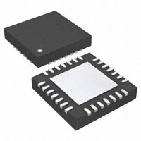


 工商网监
湘ICP备2023018690号
工商网监
湘ICP备2023018690号
