Not Recommended for New Designs
bq29410, bq29411, bq29412
bq29413, bq29414
bq29415, bq29419
www.ti.com
SLUS669G – AUGUST 2005 – REVISED AUGUST 2008
VOLTAGE PROTECTION FOR 2-, 3-, OR 4-CELL Li-Ion BATTERIES
(2nd-LEVEL PROTECTION)
Check for Samples: bq29410, bq29411, bq29412, bq29413, bq29414, bq29415, bq29419
FEATURES
DESCRIPTION
•
•
The bq2941x is a secondary overvoltage protection
IC for 2-, 3-, or 4-cell lithium-ion battery packs that
incorporates a high-accuracy precision overvoltage
detection circuit. It includes a programmable delay
circuit for overvoltage detection time.
1
•
•
•
•
2-, 3-, or 4-Cell Secondary Protection
Low Power Consumption ICC < 2 µA
[VCELL(ALL) < V(PROTECT)]
Fixed High Accuracy Overvoltage Protection
Threshold
– bq29410 = 4.35 V
– bq29411 = 4.40 V
– bq29412 = 4.45 V
– bq29413 = 4.50 V
– bq29414 = 4.55 V
– bq29415 = 4.60 V
– bq29419 = 4.30 V
Programmable Delay Time of Detection
High Power Supply Ripple Rejection
Stable During Pulse Charge Operation
APPLICATIONS
•
nd
2 -Level Overvoltage Protection in Li-Ion
Battery Packs in:
– Notebook Computers
– Portable Instrumentation
– Portable Equipment
FUNCTION
Each cell in a multiple-cell pack is compared to an
internal reference voltage. If one cell reaches an
overvoltage condition, the protection sequence
begins. The bq2941x device starts charging an
external capacitor through the CD pin. When the CD
pin voltage reaches 1.2 V, the OUT pin changes from
a low level to a high level.
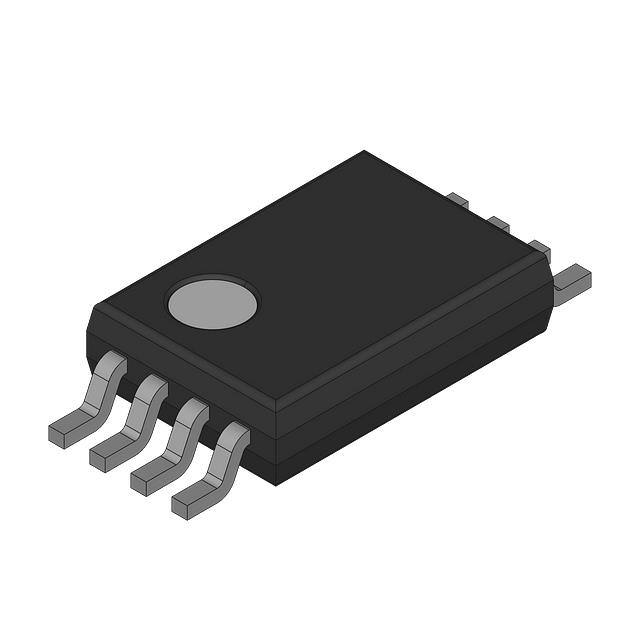
DCT PACKAGE
(TOP VIEW)
OUT
VDD
CD
1
8
2
7
3
6
VC1
VC2
VC3
VC4
4
5
GND
PW PACKAGE
(TOP VIEW)
VC1
VC2
VC3
GND
1
2
3
4
8
7
6
5
OUT
VDD
CD
VC4
1
Please be aware that an important notice concerning availability, standard warranty, and use in critical applications of
Texas Instruments semiconductor products and disclaimers thereto appears at the end of this data sheet.
PRODUCTION DATA information is current as of publication date.
Products conform to specifications per the terms of the Texas
Instruments standard warranty. Production processing does not
necessarily include testing of all parameters.
Copyright © 2005–2008, Texas Instruments Incorporated
�bq29410, bq29411, bq29412
bq29413, bq29414
bq29415, bq29419
Not Recommended for New Designs
SLUS669G – AUGUST 2005 – REVISED AUGUST 2008
www.ti.com
This integrated circuit can be damaged by ESD. Texas Instruments recommends that all integrated circuits be handled with
appropriate precautions. Failure to observe proper handling and installation procedures can cause damage.
ESD damage can range from subtle performance degradation to complete device failure. Precision integrated circuits may be more
susceptible to damage because very small parametric changes could cause the device not to meet its published specifications.
ORDERING INFORMATION (1)
TA
V(PROTECT)
PACKAGE (3)
(2)
MSOP (DCT)
SYMBOL
bq29419DCTR
4.30 V
bq29419DCTT
SSOP (PW)
CJQ
bq29419PWG4
bq29419PWRG4
CJG
bq29410PW
bq29410PWG4
bq29410PWR
bq29410PWRG4
CJH
bq29411PW
bq29411PWG4
bq29411PWR
bq29411PWRG4
CJJ
bq29412PW
bq29412PWG4
bq29412PWR
bq29412PWRG4
CJk
bq29413PW
bq29413PWR
CJL
bq29414PW
bq29414PWR
CJM
bq29415PW
bq29415PWR
bq29410DCT3R
4.35 V
bq29410DCTR
bq29410DCTT
bq29411DCT3R
4.40 V
bq29411DCTR
bq29411DCTT
–40°C to 110°C
bq29412DCT3R
4.45 V
bq29412DCTR
bq29412DCTT
4.50 V
4.55 V
4.60 V
(1)
(2)
(3)
bq29413DCTR
bq29413DCTT
bq29414DCTR
bq29414DCTT
bq29415DCTR
bq29415DCTT
For the most current package and ordering information, see the Package Option Addendum at the end of this document, or see the TI
website at www.ti.com.
Contact your local Texas Instruments representative or sales office for alternative overvoltage threshold options.
The "R" suffix indicates tape-and-reel packaging.
ABSOLUTE MAXIMUM RATINGS
over operating free-air temperature range unless otherwise noted (1)
(2)
UNIT
Supply voltage range
Input voltage range
Output voltage range
VDD
–0.3 V to 28 V
VC1, VC2, VC3, VC4
–0.3 V to 28 V
VC1 TO VC2, VC2 TO VC3, VC3 TO VC4, VC4 TO GND
–0.3 V to 8 V
OUT
–0.3 V to 28 V
CD
–0.3 V to 28 V
Continuous total power dissipation
See Dissipation Rating Table
Storage temperature range, Tstg
–65°C to 150°C
Lead temperature (soldering, 10 s)
(1)
(2)
300°C
Stresses beyond those listed under "absolute maximum ratings" may cause permanent damage to the device. These are stress ratings
only, and functional operation of the device at these or any other conditions beyond those indicated under "recommended operating
conditions" is not implied. Exposure to absolute-maximum-rated conditions for extended periods may affect device reliability.
All voltages are with respect to ground of this device except the differential voltage of VC1-VC2, VC2-VC3, VC3-VC4, and VC4-GND.
PACKAGE DISSIPATION RATINGS
2
PACKAGE
TA = 25°C
POWER RATING
DERATING FACTOR
ABOVE TA = 25°C
TA = 70°C
POWER RATING
TA = 85°C
POWER RATING
DCT
412 mW
3.3 mW/°C
264 mW
214 mW
PW
525 mW
4.2 mW/°C
336 mW
273 mW
Submit Documentation Feedback
Copyright © 2005–2008, Texas Instruments Incorporated
Product Folder Links: bq29410 bq29411 bq29412 bq29413 bq29414 bq29415 bq29419
�Not Recommended for New Designs
www.ti.com
bq29410, bq29411, bq29412
bq29413, bq29414
bq29415, bq29419
SLUS669G – AUGUST 2005 – REVISED AUGUST 2008
RECOMMENDED OPERATING CONDITIONS
MIN
VDD
Supply voltage
NOM
MAX
4
25
VC1, VC2, VC3, VC4
0
25
VCn – VC (n=1), (n=1, 2, 3), VC4 – GND
0
5
UNIT
V
VI
Input voltage range
td(CD)
Delay time capacitance
RIN
Voltage-monitor filter resistance
100
1k
Ω
CIN
Voltage-monitor filter capacitance
0.01
0.1
µF
RVD
Supply-voltage filter resistance
CVD
Supply-voltage filter capacitance
TA
Operating ambient temperature range
0.22
V
µF
0
1
0.1
kΩ
µF
–40
110
°C
ELECTRICAL CHARACTERISTICS
over recommended operating free-air temperature range, TA = 25°C (unless otherwise noted)
PARAMETER
V(OA)
Overvoltage detection
accuracy
TEST CONDITION
MIN
NOM MAX
TA = 25°C
25
35
TA = –20°C to 85°C
25
50
TA = –40°C to 110°C
V(PROTECT)
Overvoltage
detection voltage
4.35
bq29411
4.40
bq29412
4.45
bq29413
4.50
bq29414
4.55
bq29415
4.60
bq29419
4.30
bq29410/11/12/13/14/15
IIN
Input current
V2, V3 , VC4 input ,VDD = VC1
VC1 = VC2 = VC3 = VC4 = 3.5 V (see Figure 1)
tD1
Overvoltage detection delay
time
VDD = VC1, CD = 0.22 µF
1
1.5
I(CD_dis)
CD GND clamp current
VDD = VC1, CD = 1 V
5
12
V(OUT)
OUT pin drive voltage
bq29419
250
320
VDD = VC1,
VC1–VC2 = VC2–VC3 = VC3–VC4 = VC4–GND = 3.5 V
(see Figure 1)
2
VDD = VC1,
VC1–VC2 = VC2–VC3 = VC3–VC4 = VC4–GND = 2.3 V
(see Figure 1)
1.5
450
mV
0.3
µA
2
S
µA
3
µA
VC1–VC2 = VC2–VC3 = VC3–VC4 = VC4–GND =
V(PROTECT)Max, VDD = 14 V, IOH = 0 mA
2.5
7
V
VC1 = VC2 = VC3 = VC4 = V(PROTECT)Max,
VDD = 4.3 V, TA = 0°C to 70°C, IOH = 40 μA
1.5
IOH
High-level output current
OUT = 3 V,
VC1–VC2 = VC2–VC3 = VC3–VC4 = VC4–GND =
V(PROTECT)Max, VDD = 14 V
IOL
Low-level output current
OUT = 0.1 V, VDD = VC1,
VC1–VC2 = VC2–VC3 = VC3–VC4 = VC4–GND = 3.5 V
Copyright © 2005–2008, Texas Instruments Incorporated
V
320
Overvoltage detection
hysteresis
Supply current
mV
80
bq29410
Vhys
ICC
UNIT
2
2.5
–1
5
Submit Documentation Feedback
Product Folder Links: bq29410 bq29411 bq29412 bq29413 bq29414 bq29415 bq29419
mA
µA
3
�Not Recommended for New Designs
bq29410, bq29411, bq29412
bq29413, bq29414
bq29415, bq29419
SLUS669G – AUGUST 2005 – REVISED AUGUST 2008
www.ti.com
1 OUT
VC1
VC1 8
2 VDD
VC2
VC2 8
7
3 CD
VC3
VC3 6
4 VC4
GND
GND 5
Figure 1. ICC, IIN Measurement (DCT Package)
Terminal Functions
TERMINAL
4
DESCRIPTION
MSOP
(DCT)
TSSOP
(PW)
NAME
8
1
VC1
Sense voltage input for most positive cell
7
2
VC2
Sense voltage input for second most positive cell
6
3
VC3
Sense voltage input for third most positive cell
5
4
GND
Ground pin
4
5
VC4
Sense voltage input for least positive cell
3
6
CD
An external capacitor is connected to determine the programmable delay time
2
7
VDD
Power supply
1
8
OUT
Output
Submit Documentation Feedback
Copyright © 2005–2008, Texas Instruments Incorporated
Product Folder Links: bq29410 bq29411 bq29412 bq29413 bq29414 bq29415 bq29419
�Not Recommended for New Designs
www.ti.com
bq29410, bq29411, bq29412
bq29413, bq29414
bq29415, bq29419
SLUS669G – AUGUST 2005 – REVISED AUGUST 2008
FUNCTIONAL BLOCK DIAGRAM
RVD
CVD
VDD
VC1
RIN
ICD = 0.2 A (TYP)
CIN
RIN
VC2
CIN
VC3
OUT
RIN
CIN
VC4
1.2 V (TYP)
RIN
CIN
GND
CD
C(DELAY)
OVERVOLTAGE PROTECTION
When one of the cell voltages exceeds V(PROTECT), an internal current source begins to charge the capacitor,
C(DELAY), connected to the CD pin. If the voltage at the CD pin, VCD, reaches 1.2 V, the OUT pin is activated and
transitions high. An externally connected NCH FET is activiated and blows the external fuse in the positive
battery rail; see the functional block diagram.
If all cell voltages fall below V(PROTECT) before the voltage at pin CD reaches 1.2 V, the delay time does not run
out. An internal switch clamps the CD pin to GND and discharges the capacitor, C(DELAY), and secures the full
delay time for the next occurring overvoltage event.
Once the pin OUT is activated, it transitions back from high to low after all battery cells reach V(PROTECT) – Vhys.
DELAY TIME CALCULATION
The delay time is calculated as follows:
t +
d
C
ƪ1.2 V
(DELAY)
C
I
+
(DELAY)
ƫ
CD
ƪtd
I
ƫ
CD
1.2 V
Where I(CD) = CD current source = 0.18 µA
Copyright © 2005–2008, Texas Instruments Incorporated
Submit Documentation Feedback
Product Folder Links: bq29410 bq29411 bq29412 bq29413 bq29414 bq29415 bq29419
5
�bq29410, bq29411, bq29412
bq29413, bq29414
bq29415, bq29419
Not Recommended for New Designs
SLUS669G – AUGUST 2005 – REVISED AUGUST 2008
www.ti.com
V(PROTECT)
V(PROTECT) - Vhys
Cell Voltage
(VCn - VC(n-1),
VC4 - GND)
1.2 V
CD
tDELAY
OUT
td = (1.2 V x CDELAY)/ICD
Figure 2. Timing for Overvoltage Sensing
APPLICATION INFORMATION
BATTERY CONNECTIONS
The following diagrams show the DCT package device in different cell configurations.
1 OUT
VC1 8
1 OUT
VC1 8
2 VDD
VC2 8
7
2 VDD
7
VC2 8
3 CD
VC3 6
3 CD
2
VC3 6
4 VC4
GND 5
4 VC4
2
GND 5
Figure 3. 4-Series Cell Configuration
6
Submit Documentation Feedback
Figure 4. 3-Series Cell Configuration
(Connect together VC1 and VC2)
Copyright © 2005–2008, Texas Instruments Incorporated
Product Folder Links: bq29410 bq29411 bq29412 bq29413 bq29414 bq29415 bq29419
�Not Recommended for New Designs
www.ti.com
bq29410, bq29411, bq29412
bq29413, bq29414
bq29415, bq29419
SLUS669G – AUGUST 2005 – REVISED AUGUST 2008
1 OUT
VC1 8
2 VDD
VC2 77
36 CD
VC3 6
4 VC4
GND 5
Figure 5. 2-Series Cell Configuration
CELL CONNECTIONS
To prevent incorrect output activation, the following connection sequences must be used.
4-Series Cell Configuration
• VC1(=VDD) → VC2 → VC3 → VC4 → GND or
• GND → VC4 → VC3 → VC2 → VC1(=VDD)
3-Series Cell Configuration
• VC1(=VC2=VDD) → VC3 → VC4 → GND or
• GND → VC4 → VC3 → VC1(=VC2=VDD)
2-Series Cell Configuration
• VC1(=VC2=VC3=VDD) → VC4 → GND or
• GND → VC4 → VC1(=VC2=VC3=VDD)
Copyright © 2005–2008, Texas Instruments Incorporated
Submit Documentation Feedback
Product Folder Links: bq29410 bq29411 bq29412 bq29413 bq29414 bq29415 bq29419
7
�PACKAGE OPTION ADDENDUM
www.ti.com
23-Aug-2017
PACKAGING INFORMATION
Orderable Device
Status
(1)
Package Type Package Pins Package
Drawing
Qty
Eco Plan
Lead/Ball Finish
MSL Peak Temp
(2)
(6)
(3)
Op Temp (°C)
Device Marking
(4/5)
BQ29410DCT3R
NRND
SM8
DCT
8
3000
Pb-Free
(RoHS)
CU SNBI
Level-1-260C-UNLIM
-40 to 110
CJG
W
BQ29410DCT3RE6
NRND
SM8
DCT
8
3000
Pb-Free
(RoHS)
CU SNBI
Level-1-260C-UNLIM
-40 to 110
CJG
W
BQ29410DCTR
NRND
SM8
DCT
8
3000
Green (RoHS
& no Sb/Br)
CU NIPDAU
Level-1-260C-UNLIM
-40 to 110
CJG
W
BQ29410DCTRG4
NRND
SM8
DCT
8
3000
Green (RoHS
& no Sb/Br)
CU NIPDAU
Level-1-260C-UNLIM
-40 to 110
CJG
W
BQ29410DCTT
NRND
SM8
DCT
8
250
Green (RoHS
& no Sb/Br)
CU NIPDAU
Level-1-260C-UNLIM
-40 to 110
CJG
W
BQ29410DCTTG4
NRND
SM8
DCT
8
250
Green (RoHS
& no Sb/Br)
CU NIPDAU
Level-1-260C-UNLIM
-40 to 110
CJG
W
BQ29410PW
NRND
TSSOP
PW
8
150
Green (RoHS
& no Sb/Br)
CU NIPDAU
Level-1-260C-UNLIM
-40 to 110
29410
BQ29410PWR
NRND
TSSOP
PW
8
2000
Green (RoHS
& no Sb/Br)
CU NIPDAU
Level-1-260C-UNLIM
-40 to 110
29410
BQ29410PWRG4
NRND
TSSOP
PW
8
2000
Green (RoHS
& no Sb/Br)
CU NIPDAU
Level-2-260C-1 YEAR
-40 to 110
29410
BQ29411DCT3R
NRND
SM8
DCT
8
3000
Pb-Free
(RoHS)
CU SNBI
Level-1-260C-UNLIM
-40 to 110
CJH
W
BQ29411DCTR
NRND
SM8
DCT
8
3000
Green (RoHS
& no Sb/Br)
CU NIPDAU
Level-1-260C-UNLIM
-40 to 110
CJH
W
BQ29411DCTRG4
NRND
SM8
DCT
8
3000
Green (RoHS
& no Sb/Br)
CU NIPDAU
Level-1-260C-UNLIM
-40 to 110
CJH
W
BQ29411DCTT
NRND
SM8
DCT
8
250
Green (RoHS
& no Sb/Br)
CU NIPDAU
Level-1-260C-UNLIM
-40 to 110
CJH
W
BQ29411PW
NRND
TSSOP
PW
8
150
Green (RoHS
& no Sb/Br)
CU NIPDAU
Level-1-260C-UNLIM
-40 to 110
29411
BQ29411PWRG4
NRND
TSSOP
PW
8
2000
Green (RoHS
& no Sb/Br)
CU NIPDAU
Level-2-260C-1 YEAR
-40 to 110
29411
BQ29412DCT3R
NRND
SM8
DCT
8
3000
Pb-Free
(RoHS)
CU SNBI
Level-1-260C-UNLIM
-40 to 110
CJJ
W
BQ29412DCT3RE6
NRND
SM8
DCT
8
3000
Pb-Free
(RoHS)
CU SNBI
Level-1-260C-UNLIM
-40 to 110
CJJ
W
Addendum-Page 1
Samples
�PACKAGE OPTION ADDENDUM
www.ti.com
23-Aug-2017
Orderable Device
Status
(1)
Package Type Package Pins Package
Drawing
Qty
Eco Plan
Lead/Ball Finish
MSL Peak Temp
(2)
(6)
(3)
Op Temp (°C)
Device Marking
(4/5)
BQ29412DCTR
NRND
SM8
DCT
8
3000
Green (RoHS
& no Sb/Br)
CU NIPDAU
Level-1-260C-UNLIM
-40 to 110
CJJ
W
BQ29412DCTRG4
NRND
SM8
DCT
8
3000
Green (RoHS
& no Sb/Br)
CU NIPDAU
Level-1-260C-UNLIM
-40 to 110
CJJ
W
BQ29412DCTT
NRND
SM8
DCT
8
250
Green (RoHS
& no Sb/Br)
CU NIPDAU
Level-1-260C-UNLIM
-40 to 110
CJJ
W
BQ29412DCTTG4
NRND
SM8
DCT
8
250
Green (RoHS
& no Sb/Br)
CU NIPDAU
Level-1-260C-UNLIM
-40 to 110
CJJ
W
BQ29412PW
NRND
TSSOP
PW
8
150
Green (RoHS
& no Sb/Br)
CU NIPDAU
Level-1-260C-UNLIM
-40 to 110
29412
BQ29412PWR
NRND
TSSOP
PW
8
2000
Green (RoHS
& no Sb/Br)
CU NIPDAU
Level-1-260C-UNLIM
29412
BQ29412PWRG4
NRND
TSSOP
PW
8
2000
Green (RoHS
& no Sb/Br)
CU NIPDAU
Level-2-260C-1 YEAR
29412
BQ29413DCTR
NRND
SM8
DCT
8
3000
Green (RoHS
& no Sb/Br)
CU NIPDAU
Level-1-260C-UNLIM
-40 to 110
CJK
W
BQ29413DCTRG4
NRND
SM8
DCT
8
3000
Green (RoHS
& no Sb/Br)
CU NIPDAU
Level-1-260C-UNLIM
-40 to 110
CJK
W
BQ29413DCTT
NRND
SM8
DCT
8
250
Green (RoHS
& no Sb/Br)
CU NIPDAU
Level-1-260C-UNLIM
-40 to 110
CJK
W
BQ29413PWR
NRND
TSSOP
PW
8
2000
Green (RoHS
& no Sb/Br)
CU NIPDAU
Level-2-260C-1 YEAR
-40 to 110
29413
BQ29415PWR
NRND
TSSOP
PW
8
2000
Green (RoHS
& no Sb/Br)
CU NIPDAU
Level-2-260C-1 YEAR
-40 to 110
2915
BQ29419PW
NRND
TSSOP
PW
8
150
Green (RoHS
& no Sb/Br)
CU NIPDAU
Level-2-260C-1 YEAR
-40 to 110
29419
BQ29419PWG4
NRND
TSSOP
PW
8
150
Green (RoHS
& no Sb/Br)
CU NIPDAU
Level-2-260C-1 YEAR
-40 to 110
29419
BQ29419PWR
NRND
TSSOP
PW
8
2000
Green (RoHS
& no Sb/Br)
CU NIPDAU
Level-2-260C-1 YEAR
-40 to 110
29419
(1)
The marketing status values are defined as follows:
ACTIVE: Product device recommended for new designs.
LIFEBUY: TI has announced that the device will be discontinued, and a lifetime-buy period is in effect.
NRND: Not recommended for new designs. Device is in production to support existing customers, but TI does not recommend using this part in a new design.
PREVIEW: Device has been announced but is not in production. Samples may or may not be available.
OBSOLETE: TI has discontinued the production of the device.
Addendum-Page 2
Samples
�PACKAGE OPTION ADDENDUM
www.ti.com
23-Aug-2017
(2)
RoHS: TI defines "RoHS" to mean semiconductor products that are compliant with the current EU RoHS requirements for all 10 RoHS substances, including the requirement that RoHS substance
do not exceed 0.1% by weight in homogeneous materials. Where designed to be soldered at high temperatures, "RoHS" products are suitable for use in specified lead-free processes. TI may
reference these types of products as "Pb-Free".
RoHS Exempt: TI defines "RoHS Exempt" to mean products that contain lead but are compliant with EU RoHS pursuant to a specific EU RoHS exemption.
Green: TI defines "Green" to mean the content of Chlorine (Cl) and Bromine (Br) based flame retardants meet JS709B low halogen requirements of


 工商网监
湘ICP备2023018690号
工商网监
湘ICP备2023018690号
