bq4845/bq4845Y
Parallel RTC With CPU Supervisor
General Description
Features
➤ Real-Time Clock counts seconds
through years in BCD format
➤ On-chip battery-backup switchover
circuit with nonvolatile control for
external SRAM
➤ Less than 500nA of clock operation current in backup mode
➤ Microprocessor reset valid to
VCC = VSS
➤ Independent watchdog timer
with a programmable time-out
period
➤ Power-fail interrupt warning
➤ Programmable clock alarm interrupt active in battery-backup
mode
➤ Programmable periodic interrupt
28
27
26
25
24
23
22
21
20
19
18
17
16
15
The bq4845 also has a built-in
watchdog timer to monitor processor
operation. If the microprocessor does
not toggle the watchdog input (WDI)
within the programmed time-out period, the bq4845 asserts WDO and
RST. WDI unconnected disables the
watchdog timer.
The bq4845 can generate other interrupts based on a clock alarm condition or a periodic setting. The
alarm interrupt can be set to occur
from once per second to once per
month. The alarm can be made active
in the battery-backup mode to serve
as a system wake-up call. For interrupts at a rate beyond once per second, the periodic interrupt can be programmed with periods of 30.5µs to
500ms.
Pin Names
Pin Connections
1
2
3
4
5
6
7
8
9
10
11
12
13
14
The bq4845 provides direct connections for a 32.768KHz quartz crystal
and a 3V backup battery. Through
the use of the conditional chip enable output (CE OUT ) and battery
voltage output (V OUT ) pins, the
bq4845 can write-protect and make
nonvolatile external SRAMs. The
backup cell powers the real-time
clock and maintains SRAM information in the absence of system
voltage.
The bq4845 contains a temperaturecompensated reference and comparator
circuit that monitors the status of its
voltage supply. When the bq4845 de-
➤ Battery-low warning
VOUT
X1
X2
WDO
INT
RST
A3
A2
A1
A0
DQ0
DQ1
DQ2
VSS
The bq4845 Real-Time Clock is a
low-power microprocessor peripheral that integrates a time-of-day
clock, a 100-year calendar, and a
CPU supervisor in a 28-pin SOIC or
DIP. The bq4845 is ideal for fax machines, copiers, industrial control
systems, point-of-sale terminals,
data loggers, and computers.
tects an out-of-tolerance condition, it
generates an interrupt warning and
subsequently a microprocessor reset.
The reset stays active for 200ms after
VCC rises within tolerance, to allow for
power supply and processor stabilization.
VCC
WE
CEIN
CEOUT
BC
WDI
OE
CS
VSS
DQ7
DQ8
DQ5
DQ4
DQ3
A0–A3
Clock/control address
inputs
BC
Backup battery input
DQ0–DQ7
Data inputs/outputs
VOUT
Back-up battery output
WE
Write enable
INT
Interrupt output
OE
Output enable
RST
Microprocessor reset
CS
Chip select input
WDI
Watchdog input
CEIN
External RAM chip
enable
WDO
Watchdog output
CEOUT
Conditional RAM chip
enable
VCC
+5V supply
VSS
Ground
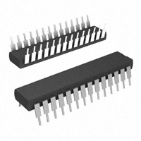
28-DIP or SOIC
PN484501.eps
X1–X2
Crystal inputs
Aug. 1995
1
�bq4845/bq4845Y
power-on reset timing, watchdog timer activation, and
interrupt generation.
Functional Description
Figure 1 is a block diagram of the bq4845. The following sections describe the bq4845 functional operation
including clock interface, data-retention modes,
Figure 1. Block Diagram
Truth Table
VCC
CS
OE
WE
CEOUT
VOUT
Mode
DQ
Power
< VCC (max.)
VIH
X
X
CEIN
VOUT1
Deselect
High Z
Standby
VIL
X
VIL
CEIN
VOUT1
Write
DIN
Active
> VCC (min.)
VIL
VIL
VIH
CEIN
VOUT1
Read
DOUT
Active
VIL
VIH
VIH
CEIN
VOUT1
Read
High Z
Active
< VPFD (min.) > VSO
X
X
X
VOH
VOUT1
Deselect
High Z
CMOS standby
≤ VSO
X
X
X
VOHB
VOUT2
Deselect
High Z
Battery-backup mode
Aug. 1995
2
�bq4845/bq4845Y
DQ0–DQ7 Data input and output
Pin Descriptions
X1–X2
X1–X2 are a direct connection
32.768kHZ, 6pF crystal.
RST
DQ0–DQ7 provide x8 data for real-time clock
information. These pins connect to the memory data bus.
Crystal inputs
for
a
Reset output
RST goes low whenever VCC falls below the
power fail threshold. RST will remain low for
200ms typical after VCC crosses the threshold
on power-up. RST also goes low whenever a
watchdog timeout occurs. RST is an opendrain output.
INT
VSS
Ground
CS
Chip select
OE
Output enable
OE provides the read control for the RTC
memory locations.
CEOUT
Interrupt output
CEOUT goes low only when CEIN is low and
VCC is above the power fail threshold. If
CEIN is low, and power fail occurs, CEOUT
stays low for 100µs or until CEIN goes high,
whichever occurs first.
INT goes low when a power fail, periodic, or
alarm condition occurs. INT is an open-drain
output.
WDI
Watchdog input
CEIN
WDI is a three-level input. If WDI remains
either high or low for longer than the
watchdog time-out period (1.5 seconds default), WDO goes low. WDO remains low
until the next transition at WDI. Leaving
WDI unconnected disables the watchdog
function. WDI connects to an internal voltage divider between VOUT and VSS, which
sets it to mid-supply when left unconnected.
WDO
Chip enable input
CEIN is the input to the chip-enable gating
circuit.
BC
Backup battery input
BC should be connected to a 3V backup
cell. A voltage within the VBC range on the
BC pin should be present upon power up to
provide proper oscillator start-up.
VOUT
Watchdog output
Output supply voltage
VOUT provides the higher of VCC or VBC,
switched internally, to supply external
RAM.
WDO goes low if WDI remains either high
or low longer than the watchdog time-out
period. WDO returns high on the next transition at WDI. WDO remains high if WDI is
unconnected.
A0–A3
Chip enable output
WE
Write enable
WE provides the write control for the RTC
memory locations.
Clock address inputs
VCC
A0–A3 allow access to the 16 bytes of realtime clock and control registers.
Input supply voltage
+5V input
Aug. 1995
3
�bq4845/bq4845Y
Address Map
Read Mode
The bq4845 provides 16 bytes of clock and control status
registers. Table 1 is a map of the bq4845 registers, and
Table 2 describes the register bits.
The bq4845 is in read mode whenever OE (Output enable) is low and CS (chip select) is low. The unique address, specified by the 4 address inputs, defines which
one of the 16 clock/calendar bytes is to be accessed. The
bq4845 makes valid data available at the data I/O pins
within tAA (address access time). This occurs after the
last address input signal is stable, and providing the CS
and OE (output enable) access times are met. If the CS
and OE access times are not met, valid data is available
after the latter of chip select access time (tACS) or output
enable access time (tOE).
Clock Memory Interface
The bq4845 has the same interface for clock/calendar
and control information as standard SRAM. To read and
write to these locations, the user must put the bq4845 in
the proper mode and meet the timing requirements.
CS and OE control the state of the eight three-state
data I/O signals. If the outputs are activated before tAA,
Table 1. bq4845 Clock and Control Register Map
Address
(h)
0
D7
0
1
ALM1
2
0
3
ALM1
4
PM/AM
ALM1
PM/AM
0
ALM1
0
0
5
6
7
8
9
A
B
*
C
*
D
E
F
*
*
*
Notes:
D6
D5
D4
10-second digit
ALM0
10-second digit
10-minute digit
ALM0
10-minute digit
0
10-hour digit
ALM0
D3
10-hour digit
0
ALM0
10-day digit
10-day digit
0
0
0
10 mo.
10-year digit
WD2
*
WD1
WD0
0
12-Hour
Range (h)
00–59
Register
Seconds
1-second digit
00–59
Seconds alarm
1-minute digit
00–59
Minutes
1-minute digit
00–59
Minutes alarm
D2
D1
1-second digit
D0
1-hour digit
01–12 AM/ 81– 92 PM Hours
1-hour digit
01–12 AM/ 81–92 PM Hours alarm
1-day digit
1-day digit
Day-of-week digit
1-month digit
1-year digit
RS3
RS2
*
AIE
PIE
PWRIE ABE
*
*
*
AF
UTI
*
PF
STOP
*
PWRF BVF
24/12 DSE
*
*
*
RS1
RS0
01–31
01–31
01–07
01–12
00–99
Day
Day alarm
Day-of-week
Month
Year
Programmable
rates
Interrupt enables
Flags
Control
Unused
* = Unused bits; unwritable and read as 0.
0 = should be set to 0 for valid time/calendar range.
Clock calendar data in BCD. Automatic leap year adjustment.
PM/AM = 1 for PM; PM/AM = 0 for AM.
DSE = 1 enables daylight savings adjustment.
24/12 = 1 enables 24-hour data representation; 24/12 = 0 enables 12-hour data representation.
Day-of-Week coded as Sunday = 1 through Saturday = 7.
BVF = 1 for valid battery.
STOP = 1 turns the RTC on; STOP = 0 stops the RTC in back-up mode.
Aug. 1995
4
�bq4845/bq4845Y
Reading the Clock
Table 2. Clock and Control Register Bits
ABE
Alarm interrupt enable in
battery-backup mode
AF
Alarm interrupt flag
AIE
Alarm interrupt enable
ALM0–ALM1
Alarm mask bits
BVF
Battery-valid flag
DSE
Daylight savings time enable
PF
Periodic interrupt flag
PIE
Periodic interrupt enable
Once every second, the user-accessible clock/calendar locations are updated simultaneously from the internal
real time counters. To prevent reading data in transition, updates to the bq4845 clock registers should be
halted. Updating is halted by setting the update transfer inhibit (UTI) bit D3 of the control register E. As long
as the UTI bit is 1, updates to user-accessible clock locations are inhibited. Once the frozen clock information is
retrieved by reading the appropriate clock memory locations, the UTI bit should be reset to 0 in order to allow
updates to occur from the internal counters. Because
the internal counters are not halted by setting the UTI
bit, reading the clock locations has no effect on clock accuracy. Once the UTI bit is reset to 0, the internal registers update within one second the user-accessible registers with the correct time. A halt command issued during a clock update allows the update to occur before
freezing the data.
PM/AM
PM or AM indication
Setting the Clock
PWRF
Power-fail interrupt flag
PWRIE
Power-fail interrupt enable
RS0–RS3
Periodic interrupt rate
STOP
Oscillator stop and start
The UTI bit must also be used to set the bq4845 clock.
Once set, the locations can be written with the desired
information in BCD format. Resetting the UTI bit to 0
causes the written values to be transferred to the internal clock counters and allows updates to the useraccessible registers to resume within one second.
UTI
Update transfer inhibit
WD0 - WD2
Watchdog time-out rate
Bits
24/12
Description
24- or 12-hour representation
Stopping and Starting the Clock Oscillator
The bq4845 clock can be programmed to turn off when
the part goes into battery back-up mode by setting
STOP to 0 prior to power down. If the board using the
bq4845 is to spend a significant period of time in storage, the STOP bit can be used to preserve some battery
capacity. STOP set to 1 keeps the clock running when
VCC drops below VSO. With VCC greater than VSO, the
bq4845 clock runs regardless of the state of STOP.
the data lines are driven to an indeterminate state until
tAA. If the address inputs are changed while CS and OE
remain low, output data remains valid for tOH (output
data hold time), but goes indeterminate until the next
address access.
Write Mode
Power-Down/Power-Up Cycle
The bq4845 is in write mode whenever WE and CS are
active. The start of a write is referenced from the
latter-occurring falling edge of WE or CS. A write is terminated by the earlier rising edge of WE or CS. The addresses must be held valid throughout the cycle. CS or
WE must return high for a minimum of tWR2 from CS or
tWR1 from WE prior to the initiation of another read or
write cycle.
The bq4845 continuously monitors V CC for out-oftolerance. During a power failure, when VCC falls below
VPFD, the bq4845 write-protects the clock and storage
registers. When VCC is below VBC (3V typical), the
power source is switched to BC. RTC operation and
storage data are sustained by a valid backup energy
source. When VCC is above VBC, the power source is
VCC. Write-protection continues for tCSR time after VCC
rises above VPFD.
Data-in must be valid tDW prior to the end of write and
remain valid for tDH1 or tDH2 afterward. OE should be
kept high during write cycles to avoid bus contention; although, if the output bus has been activated by a low on
CS and OE, a low on WE disables the outputs tWZ after
WE falls.
An external CMOS static RAM is battery-backed using
the VOUT and chip enable output pins from the bq4845.
As the voltage input VCC slews down during a power
failure, the chip enable output, CEOUT, is forced inactive
independent of the chip enable input CEIN.
Aug. 1995
5
�bq4845/bq4845Y
This activity unconditionally write-protects the external
SRAM as VCC falls below VPFD. If a memory access is in
progress to the external SRAM during power-fail detection, that memory cycle continues to completion before
the memory is write-protected. If the memory cycle is
not terminated within time tWPT, the chip enable output
is unconditionally driven high, write-protecting the controlled SRAM.
A primary backup energy source input is provided on
the bq4845. The BC input accepts a 3V primary battery,
typically some type of lithium chemistry. Since the
bq4845 provides for reverse battery charging protection,
no diode or current limiting resistor is needed in series
with the cell. To prevent battery drain when there is no
valid data to retain, VOUT and CEOUT are internally isolated from BC by the initial connection of a battery. Following the first application of VCC above VPFD, this isolation is broken, and the backup cell provides power to
VOUT and CEOUT for the external SRAM.
As the supply continues to fall past VPFD, an internal
switching device forces VOUT to the external backup energy source. CEOUT is held high by the VOUT energy
source.
The crystal should be located as close to X1 and X2 as
possible and meet the specifications in the Crystal
Specification Table. With the specified crystal, the
bq4845 RTC will be accurate to within one minute per
month at room temperature. In the absence of a crystal,
a 32.768 kHz waveform can be fed into X1 with X2
grounded.
During power-up, VOUT is switched back to the 5V supply as VCC rises above the backup cell input voltage
sourcing VOUT. CEOUT is held inactive for time tCER after the power supply has reached VPFD, independent of
the CEIN input, to allow for processor stabilization.
During power-valid operation, the CEIN input is passed
through to the CEOUT output with a propagation delay of
less than 12ns.
Power-On Reset
The bq4845 provides a power-on reset, which pulls the
RST pin low on power-down and remains low on powerup for tRST after VCC passes VPFD. With valid battery
voltage on BC, RST remains valid for VCC= VSS.
Figure 2 shows the hardware hookup for the external
RAM, battery, and crystal.
Figure 2. bq4845 Application Circuit
Aug. 1995
6
�bq4845/bq4845Y
at WDI) biases WDI to approximately 1.6V. Internal
comparators detect this level and disable the watchdog
timer. When VCC is below the power-fail threshold, the
bq4845 disables the watchdog function and disconnects
WDI from its internal resistor network, thus making it
high impedance.
Watchdog Timer
The watchdog monitors microprocessor activity through
the Watchdog input (WDI). To use the watchdog function, connect WDI to a bus line or a microprocessor I/O
line. If WDI remains high or low for longer than the
watchdog time-out period (1.5 seconds default), the
bq4845 asserts WDO and RST.
Watchdog Output
The Watchdog output (WDO) remains high if there is a
transition or pulse at WDI during the watchdog timeout period. The bq4845 disables the watchdog function
and WDO is a logic high when VCC is below the power
fail threshold, battery-backup mode is enabled, or WDI
is an open circuit. In watchdog mode, if no transition occurs at WDI during the watchdog time-out period, the
bq4845 asserts RST for the reset time-out period t1.
WDO goes low and remains low until the next transition
at WDI. If WDI is held high or low indefinitely, RST will
generate pulses (t1 seconds wide) every t3 seconds. Figure 3 shows the watchdog timing.
Watchdog Input
The bq4845 resets the watchdog timer if a change of
state (high to low, low to high, or a minimum 100ns
pulse) occurs at the Watchdog input (WDI) during the
watchdog period. The watchdog time-out is set by WD0WD2 in register B. The bq4845 maintains the watchdog
time-out programming through power cycles. The default state (no valid battery power) of WD0-WD2 is 000
or 1.5s on power-up. Table 3 shows the programmable
watchdog time-out rates. The watchdog time-out period
immediately after a reset is equal to the programmed
watchdog time-out.
To disable the watchdog function, leave WDI floating. An
internal resistor network (100kΩ equivalent impedance
Figure 3. Watchdog Time-out Period and Reset Active Time
Aug. 1995
7
�bq4845/bq4845Y
ters with the corresponding alarm registers. If a match
between all the corresponding bytes is found, the alarm
flag AF in the flags register is set. If the alarm interrupt is enabled with AIE, an interrupt request is generated on INT. The alarm condition is cleared by a read to
the flags register. ALM1 – ALM0 in the alarm registers,
mask each alarm compare byte. An alarm byte is
masked by setting ALM1 (D7) and ALM0 (D6) to 1.
Alarm byte masking can be used to select the frequency
of the alarm interrupt, according to Table 5.
Interrupts
The bq4845 allows three individually selected interrupt
events to generate an interrupt request on the INT pin.
These three interrupt events are:
■
The periodic interrupt, programmable to occur once
every 30.5µs to 500ms
■
The alarm interrupt, programmable to occur once per
second to once per month
■
The power-fail interrupt, which can be enabled to be
asserted when the bq4845 detects a power failure
The alarm interrupt can be made active while the
bq4845 is in the battery-backup mode by setting ABE in
the interrupts register. Normally, the INT pin goes
high-impedance during battery backup. With ABE set,
however, INT is driven low if an alarm condition occurs
and the AIE bit is set. Because the AIE bit is reset during power-on reset, an alarm generated during power-on
reset updates only the flags register. The user can read
the flags register during boot-up to determine if an
alarm was generated during power-on reset.
The periodic, alarm, and power-fail interrupts are enabled by an individual interrupt-enable bit in register C,
the interrupts register. When an event occurs, its event
flag bit in the flags register, register D, is set. If the corresponding event enable bit is also set, then an interrupt
request is generated. Reading the flags register clears
all flag bits and makes INT high impedance. To reset
the flag register, the bq4845 addresses must be held stable at register D for at least 50ns to avoid inadvertent
resets.
Power-Fail Interrupt
When V CC falls to the power-fail-detect point, the
power-fail flag PWRF is set. If the power-fail interrupt
enable bit (PWRIE) is also set, then INT is asserted low.
The power-fail interrupt occurs tWPT before the bq4845
generates a reset and deselects. The PWRIE bit is
cleared on power-up.
Periodic Interrupt
Bits RS3–RS0 in the interrupts register program the
rate for the periodic interrupt. The user can interpret
the interrupt in two ways: either by polling the flags
register for PF assertion or by setting PIE so that INT
goes active when the bq4845 sets the periodic flag.
Reading the flags register resets the PF bit and returns
INT to the high-impedance state. Table 4 shows the periodic rates.
Battery-Low Warning
The bq4845 checks the battery on power-up. When the
battery voltage is approximately 2.1V, the battery-valid
flag BVF in the flags register is set to a 0 indicating that
clock and RAM data may be invalid.
Alarm Interrupt
Registers 1, 3, 5, and 7 program the real-time clock
alarm. During each update cycle, the bq4845 compares
the date, hours, minutes, and seconds in the clock regis-
Table 3. Watchdog Time-out Rates
WD2
WD1
WD0
Normal Watchdog
Time-out Period (t2, t3)
Reset Time-out
Period (t1)
0
0
0
1.5s
0.25s
0
0
1
23.4375ms
3.9063ms
0
1
0
46.875ms
7.8125ms
0
1
1
93.75ms
15.625ms
1
0
0
187.5ms
31.25ms
1
0
1
375ms
62.5ms
1
1
0
750ms
125ms
1
1
1
3s
0.5s
Aug. 1995
8
�bq4845/bq4845Y
Table 4. Periodic Interrupt Rates
Register B Bits
Periodic Interrupt
RS3
RS2
RS1
RS0
Period
Units
0
0
0
0
None
0
0
0
1
30.5175
µs
0
0
1
0
61.035
µs
0
0
1
1
122.070
µs
0
1
0
0
244.141
µs
0
1
0
1
488.281
µs
0
1
1
0
976.5625
µs
0
1
1
1
1.95315
ms
1
0
0
0
3.90625
ms
1
0
0
1
7.8125
ms
1
0
1
0
15.625
ms
1
0
1
1
31.25
ms
1
1
0
0
62.5
ms
1
1
0
1
125
ms
1
1
1
0
250
ms
1
1
1
1
500
ms
Table 5. Alarm Frequency (Alarm Bits D6 and D7 of Alarm Registers)
1h
3h
5h
7h
ALM1•ALM0
ALM1•ALM0
ALM1•ALM0
ALM1•ALM0
1
1
1
1
Once per second
0
1
1
1
Once per minute when seconds match
0
0
1
1
Once per hour when minutes, and seconds match
0
0
0
1
Once per day when hours, minutes, and seconds match
0
0
0
0
When date, hours, minutes, and seconds match
Aug. 1995
9
Alarm Frequency
�bq4845/bq4845Y
Absolute Maximum Ratings
Symbol
Parameter
Value
Unit
Conditions
VCC
DC voltage applied on VCC relative to VSS
-0.3 to 7.0
V
VT
DC voltage applied on any pin excluding VCC
relative to VSS
-0.3 to 7.0
V
VT ≤ VCC + 0.3
TOPR
Operating temperature
0 to +70
°C
Commercial
-40 to +85
°C
Industrial
TSTG
Storage temperature
-55 to +125
°C
TBIAS
Temperature under bias
-40 to +85
°C
TSOLDER
Soldering temperature
+260
°C
Note:
For 10 seconds
Permanent device damage may occur if Absolute Maximum Ratings are exceeded. Functional operation
should be limited to the Recommended DC Operating Conditions detailed in this data sheet. Exposure to conditions beyond the operational limits for extended periods of time may affect device reliability.
Recommended DC Operating Conditions (TA = TOPR)
Symbol
VCC
Note:
Parameter
Supply voltage
Minimum
Typical
Maximum
Unit
4.5
5.0
5.5
V
bq4845Y
4.75
5.0
5.5
V
bq4845
0
0
0
V
VSS
Supply voltage
VIL
Input low voltage
-0.3
-
0.8
V
VIH
Input high voltage
2.2
-
VCC + 0.3
V
VBC
Backup cell voltage
2.3
-
4.0
V
Notes
Typical values indicate operation at TA = 25°C.
Aug. 1995
10
�bq4845/bq4845Y
DC Electrical Characteristics (TA = TOPR, VCCmin
Symbol
ILI
Parameter
Input leakage current
ILO
Output leakage current
VOH
VOHB
VOL
Output high voltage
VOH, BC Supply
Output low voltage
ICC
ISB1
≤ VCC ≤ VCCmax)
Minimum
-
Typical
-
Maximum
±1
Unit
µA
-
-
±1
µA
2.4
VBC- 0.3
-
-
0.4
V
V
V
Operating supply current
-
12
25
mA
Standby supply current
-
3
-
mA
ISB2
Standby supply current
-
1.5
-
mA
VSO
Supply switch-over voltage
-
VBC
-
V
ICCB
Battery operation current
-
0.3
0.5
µA
4.62
4.37
-10
20
4.75
4.5
0.4V
0.4V
0.4V
50
V
V
V
V
µA
µA
VPFD
VOUT1
VOUT2
VRST
VINT
VWDO
IWDIL
IWDIH
Notes:
Power-fail-detect voltage
Power-fail-detect voltage
VOUT voltage
VOUT voltage
RST output voltage
INT output voltage
4.55
4.30
VCC - 0.3V
VBC - 0.3V
WDO output voltage
2.4
Watchdog input low current
-50
Watchdog input high current
-
Conditions/Notes
VIN = VSS to VCC
CS = VIH or OE = VIH or WE
= VIL
IOH = -2.0 mA
VBC > VCC, IOH = -10µA
IOL = 4.0 mA
Min. cycle, duty = 100%,
CS = VIL, II/O = 0mA
CS = VIH
CS ≥ VCC - 0.2V,
0V ≤ VIN ≤ 0.2V,
or VIN ≥ VCC - 0.2V
VBC = 3V, TA = 25°C, no load
on VOUT or CEOUT
bq4845
bq4845Y
IOUT = 100mA, VCC > VBC
IOUT = 100µA, VCC < VBC
IRST = 4mA
IINT = 4mA
ISINK = 4mA
ISOURCE = 2mA
0 < VWDI < 0.8V
2.2 < VWDI < VCC
Typical values indicate operation at TA = 25°C, VCC = 5V.
RST and INT are open-drain outputs.
Crystal Specifications (DT-26 or Equivalent)
Minimum
Typical
Maximum
Unit
fO
Symbol
Oscillation frequency
Parameter
-
32.768
-
kHz
CL
Load capacitance
-
6
-
pF
TP
Temperature turnover point
20
25
30
°C
k
Parabolic curvature constant
-
-
-0.042
ppm/°C
Q
Quality factor
40,000
70,000
-
R1
Series resistance
-
-
45
KΩ
C0
Shunt capacitance
-
1.1
1.8
pF
C0/C1
Capacitance ratio
-
430
600
DL
Drive level
-
-
1
µW
∆f/fO
Aging (first year at 25°C)
-
1
-
ppm
Aug. 1995
11
�bq4845/bq4845Y
Capacitance (TA = 25°C, F = 1MHz, VCC = 5.0V)
Symbol
Parameter
Minimum
Typical
Maximum
Unit
CI/O
Input/output capacitance
-
-
7
pF
Output voltage = 0V
CIN
Input capacitance
-
-
5
pF
Input voltage = 0V
Note:
Conditions
These parameters are sampled and not 100% tested.
AC Test Conditions
Parameter
Test Conditions
Input pulse levels
0V to 3.0V
Input rise and fall times
5 ns
Input and output timing reference levels
1.5 V (unless otherwise specified)
Output load (including scope and jig)
See Figures 4 and 5
Figure 4. Output Load A
Figure 5. Output Load B
Aug. 1995
12
�bq4845/bq4845Y
Read Cycle
(TA = TOPR, VCCmin ≤ VCC ≤ VCCmax)
Symbol
Parameter
Min.
Max.
Unit
70
-
ns
Conditions
-
70
ns
Output load A
-
70
ns
Output load A
tRC
Read cycle time
tAA
Address access time
tACS
Chip select access time
tOE
Output enable to output valid
-
35
ns
Output load A
tCLZ
Chip select to output in low Z
5
-
ns
Output load B
tOLZ
Output enable to output in low Z
0
-
ns
Output load B
tCHZ
Chip deselect to output in high Z
0
25
ns
Output load B
tOHZ
Output disable to output in high Z
0
25
ns
Output load B
tOH
Output hold from address change
10
-
ns
Output load A
Write Cycle
Symbol
(TA =TOPR , VCCmin ≤ VCC ≤ VCCmax)
Parameter
Min.
Max.
Unit
tWC
Write cycle time
70
-
ns
tCW
Chip select to end of write
65
-
ns
tAW
Address valid to end of write
65
-
ns
Conditions
(1)
(1)
tAS
Address setup time
0
-
ns
Measured from address valid to beginning
of write. (2)
tWP
Write pulse width
55
-
ns
Measured from beginning of write to end of
write. (1)
tWR1
Write recovery time (write cycle 1)
5
-
ns
Measured from WE going high to end of
write cycle. (3)
tWR2
Write recovery time (write cycle 2)
15
-
ns
Measured from CS going high to end of
write cycle. (3)
tDW
Data valid to end of write
30
-
ns
Measured to first low-to-high transition of
either CS or WE.
tDH1
Data hold time (write cycle 1)
0
-
ns
Measured from WE going high to end of
write cycle. (4)
tDH2
Data hold time (write cycle 2)
10
-
ns
Measured from CS going high to end of
write cycle. (4)
tWZ
Write enabled to output in high Z
0
25
ns
I/O pins are in output state. (5)
tOW
Output active from end of write
0
-
ns
I/O pins are in output state. (5)
Notes:
1. A write ends at the earlier transition of CS going high and WE going high.
2. A write occurs during the overlap of a low CS and a low WE. A write begins at the later transition
of CS going low and WE going low.
3. Either tWR1 or tWR2 must be met.
4. Either tDH1 or tDH2 must be met.
5. If CS goes low simultaneously with WE going low or after WE going low, the outputs remain in
high-impedance state.
Aug. 1995
13
�bq4845/bq4845Y
Read Cycle No. 1 (Address Access) 1,2
Read Cycle No. 2 (CS Access) 1,3,4
Read Cycle No. 3 (OE Access) 1,5
Notes:
1. WE is held high for a read cycle.
2. Device is continuously selected: CS = OE = VIL.
3. Address is valid prior to or coincident with CS transition low.
4. OE = VIL.
5. Device is continuously selected: CS = VIL.
Aug. 1995
14
�bq4845/bq4845Y
Write Cycle No. 1 (WE-Controlled) 1,2,3
Write Cycle No. 2 (CS-Controlled) 1,2,3,4,5
Notes:
1. CS or WE must be high during address transition.
2. Because I/O may be active (OE low) during this period, data input signals of opposite polarity to the
outputs must not be applied.
3. If OE is high, the I/O pins remain in a state of high impedance.
4. Either tWR1 or tWR2 must be met.
5. Either tDH1 or tDH2 must be met.
Aug. 1995
15
�bq4845/bq4845Y
Power-Down/Power-Up Timing (TA = TOPR)
Minimum
Typical
Maximum
Unit
tF
Symbol
VCC slew from 4.75 to
4.25V
Parameter
300
-
-
µs
tFS
VCC slew from 4.25 to VSO
10
-
-
µs
tR
VCC slew from VSO to
VPFD(MAX)
100
-
-
µs
Conditions
tPF
Interrupt delay from
VPFD
6
-
24
µs
tWPT
Write-protect time for
external RAM
90
100
125
µs
Delay after VCC slews down past
VPFD before SRAM is write-protected
and RST activated.
tCSR
CS at VIH after power-up
100
200
300
ms
Internal write-protection period after VCC passes VPFD on power-up.
tRST
VPFD to RST inactive
tCSR
-
tCSR
ms
Reset active time-out period
tCER
tCED
Chip enable recovery
time
Chip enable propagation
delay to external SRAM
tCSR
-
tCSR
ms
Time during which external SRAM
is write-protected after VCC passes
VPFD on power-up.
-
9
12
ns
Output load A
Caution: Negative undershoots below the absolute maximum rating of -0.3V in battery-backup mode
may affect data integrity.
Power-Down/Power-Up Timing
Notes:
PWRIE set to “1” to enable power fail interrupt.
RST and INT are open drain and require an external pull-up resistor.
Aug. 1995
16
�bq4845/bq4845Y
28-Pin DIP (P)
28-Pin DIP (P)
Dimension
A
A1
B
B1
C
D
E
E1
e
G
L
S
Minimum
0.160
0.015
0.015
0.045
0.008
1.440
0.600
0.530
0.600
0.090
0.115
0.070
All dimensions are in inches.
Aug. 1995
17
Maximum
0.190
0.040
0.022
0.065
0.013
1.480
0.625
0.570
0.670
0.110
0.150
0.090
�bq4845/bq4845Y
28-Pin SOIC (S)
28-Pin SOIC (S)
Dimension
A
A1
B
C
D
E
e
H
L
Minimum
0.095
0.004
0.013
0.008
0.700
0.290
0.045
0.395
0.020
Maximum
0.105
0.012
0.020
0.013
0.715
0.305
0.055
0.415
0.040
All dimensions are in inches.
Aug. 1995
18
�bq4845/bq4845Y
Ordering Information
bq4845
Temperature Range:
Blank = Commercial
N = Industrial
Package Option:
P = 28-pin plastic DIP (0.600)
S = 28-pin SOIC (0.300)
Voltage Tolerance:
Blank = 5%
Y = 10%
Device:
bq4845 Real-Time Clock With CPU Supervisor
Aug. 1995
19
�PACKAGE OPTION ADDENDUM
www.ti.com
10-Dec-2020
PACKAGING INFORMATION
Orderable Device
Status
(1)
Package Type Package Pins Package
Drawing
Qty
Eco Plan
(2)
Lead finish/
Ball material
MSL Peak Temp
Op Temp (°C)
Device Marking
(3)
(4/5)
(6)
BQ4845S-A4TR
ACTIVE
SOIC
DW
28
1000
RoHS & Green
NIPDAU
Level-1-260C-UNLIM
0 to 70
4845S
-A4
(1)
The marketing status values are defined as follows:
ACTIVE: Product device recommended for new designs.
LIFEBUY: TI has announced that the device will be discontinued, and a lifetime-buy period is in effect.
NRND: Not recommended for new designs. Device is in production to support existing customers, but TI does not recommend using this part in a new design.
PREVIEW: Device has been announced but is not in production. Samples may or may not be available.
OBSOLETE: TI has discontinued the production of the device.
(2)
RoHS: TI defines "RoHS" to mean semiconductor products that are compliant with the current EU RoHS requirements for all 10 RoHS substances, including the requirement that RoHS substance
do not exceed 0.1% by weight in homogeneous materials. Where designed to be soldered at high temperatures, "RoHS" products are suitable for use in specified lead-free processes. TI may
reference these types of products as "Pb-Free".
RoHS Exempt: TI defines "RoHS Exempt" to mean products that contain lead but are compliant with EU RoHS pursuant to a specific EU RoHS exemption.
Green: TI defines "Green" to mean the content of Chlorine (Cl) and Bromine (Br) based flame retardants meet JS709B low halogen requirements of


 工商网监
湘ICP备2023018690号
工商网监
湘ICP备2023018690号
