Product
Folder
Sample &
Buy
Technical
Documents
Tools &
Software
Support &
Community
CC2560A, CC2560B, CC2564, CC2564B
SWRS121E – JULY 2012 – REVISED JANUARY 2016
CC256x Dual-Mode Bluetooth® Controller
CC2560A NRND; CC2564 NRND
1 Device Overview
1.1
Features
1
• TI's Single-Chip Bluetooth Solution With Bluetooth
Basic Rate (BR), Enhanced Data Rate (EDR), and
Low Energy (LE) Support; Available in Two
Variants:
– Dual-Mode Bluetooth CC2564 Controller
– Bluetooth CC2560 Controller
• CC2564 Bluetooth 4.1 Controller Subsystem
Qualified (QDID 58852); Compliant up to the HCI
Layer
• Highly Optimized for Low-Cost Designs:
– Single-Ended 50-Ω RF Interface
– Package Footprint: 76 Terminals, 0.6-mm Pitch,
8-mm x 8-mm mrQFN
• BR/EDR Features Include:
– Up to 7 Active Devices
– Scatternet: Up to 3 Piconets Simultaneously, 1
as Master and 2 as Slaves
– Up to 2 SCO Links on the Same Piconet
– Support for All Voice Air-Coding – Continuously
Variable Slope Delta (CVSD), A-Law, μ-Law,
and Transparent (Uncoded)
– CC2560B/CC2564B Devices Provide an
Assisted Mode for HFP 1.6 Wideband Speech
(WBS) Profile or A2DP Profile to Reduce Host
Processing and Power
– Support of Multiple Bluetooth Profiles With
Enhanced QoS
• LE Features Include:
– Support of Up to 10 (CC2564B) Connections
– Multiple Sniff Instances Tightly Coupled to
Achieve Minimum Power Consumption
– Independent Buffering for LE Allows Large
Numbers of Multiple Connections Without
Affecting BR/EDR Performance.
– Built-In Coexistence and Prioritization Handling
for BR/EDR and LE
• Best-in-Class Bluetooth (RF) Performance
1.2
•
•
•
•
•
•
•
•
•
•
•
(TX Power, RX Sensitivity, Blocking)
– Class 1 TX Power Up to +10 dBm
– –95 dbm Typical RX Sensitivity
– Internal Temperature Detection and
Compensation to Ensure Minimal Variation in
RF Performance Over Temperature, No
External Calibration Required
– Improved Adaptive Frequency Hopping (AFH)
Algorithm With Minimum Adaptation Time
– Provides Longer Range, Including 2x Range
Over Other LE-Only Solutions
Advanced Power Management for Extended
Battery Life and Ease of Design
– On-Chip Power Management, Including Direct
Connection to Battery
– Low Power Consumption for Active, Standby,
and Scan Bluetooth Modes
– Shutdown and Sleep Modes to Minimize Power
Consumption
Physical Interfaces:
– UART Interface With Support for Maximum
Bluetooth Data Rates
• UART Transport Layer (H4) With Maximum
Rate of 4 Mbps
• Three-Wire UART Transport Layer (H5) With
Maximum Rate of 4 Mbps (CC2560B and
CC2564B Only)
– Fully Programmable Digital PCM-I2S Codec
Interface
Flexibility for Easy Stack Integration and Validation
Into Various Microcontrollers, Such as MSP430™
and ARM® Cortex®-M3 and Cortex®-M4 MCUs
CC256x Bluetooth Hardware Evaluation Tool: PCBased Application to Evaluate RF Performance of
the Device and Configure Service Pack
Device Pin-to-Pin Compatible With Previous
Devices or Modules
Applications
Mobile Accessories
Sports and Fitness Applications
Wireless Audio Solutions
Remote Controls
Toys
Test and Measurement
•
•
•
•
•
Industrial: Cable Replacement
Wireless Sensors
Automotive Aftermarket
Point of Service (POS)
Wellness and Health
1
An IMPORTANT NOTICE at the end of this data sheet addresses availability, warranty, changes, use in safety-critical applications,
intellectual property matters and other important disclaimers. PRODUCTION DATA.
�CC2560A NRND; CC2564 NRND
CC2560A, CC2560B, CC2564, CC2564B
SWRS121E – JULY 2012 – REVISED JANUARY 2016
1.3
www.ti.com
Description
The TI CC256x device is a complete Bluetooth BR/EDR/LE HCI solution that reduces design effort and
enables fast time to market. Based on TI’s seventh-generation Bluetooth core, the CC256x device
provides a product-proven solution that is Bluetooth 4.1 compliant. When coupled with a microcontroller
unit (MCU), this HCI device offers best-in-class RF performance with a range of about 2X compared to
other Bluetooth LE-only solutions. Furthermore, TI’s power-management hardware and software
algorithms provide significant power savings in all commonly used Bluetooth BR/EDR/LE modes of
operation.
The TI Dual-Mode Bluetooth Stack software is certified and provided royalty free for TI's MSP430 and
ARM Cortex-M3 and Cortex-M4 MCUs. Other MPUs can be supported through TI's third party. iPod®
(MFi) protocol is supported by add-on software packages. For more information, see TI Dual-Mode
Bluetooth Stack. Some of the profiles supported include the following:
• Serial port profile (SPP)
• Advanced audio distribution profile (A2DP)
• Audio/video remote control profile (AVRCP)
• Handsfree profile (HFP)
• Human interface device (HID)
• Generic attribute profile (GATT)
• Several Bluetooth LE profiles and services
In addition to software, this solution consists of multiple reference designs with a low BOM cost, including
a new Bluetooth audio sink reference design for customers to create a variety of applications for low-end,
low-power audio solutions.
Device Information (1)
PACKAGE
BODY SIZE
CC2560A (NRND) (2)
PART NUMBER
RVM (76)
8.0 mm × 8.0 mm × 0.6 mm
CC2560B
RVM (76)
8.0 mm × 8.0 mm × 0.6 mm
RVM (76)
8.0 mm × 8.0 mm × 0.6 mm
RVM (76)
8.0 mm × 8.0 mm × 0.6 mm
CC2564 (NRND)
(2)
CC2564B
(1)
(2)
For more information on these devices, see Section 9.2, Packaging and Ordering.
NRND = Not recommended for new designs
space
2
Device Overview
Copyright © 2012–2016, Texas Instruments Incorporated
Submit Documentation Feedback
Product Folder Links: CC2560A CC2560B CC2564 CC2564B
�CC2560A NRND; CC2564 NRND
CC2560A, CC2560B, CC2564, CC2564B
www.ti.com
1.4
SWRS121E – JULY 2012 – REVISED JANUARY 2016
Functional Block Diagram
CC256x
2.4-GHz
band pass filter
Coprocessor
PCM/I2S
(See Note)
Modem
arbitrator
I/O
interface
DRP
BR/EDR
main processor
UART
HCI
Power
management
Power Shutdown
Clock
management
Slow
clock
Fast
clock
SWRS121-001
Note: The following technologies and assisted modes cannot be used simultaneously with the coprocessor: Bluetooth
LE, ANT, assisted HFP 1.6 (WBS), and assisted A2DP. One and only one technology or assisted mode can be used
at a time.
Figure 1-1. Functional Block Diagram
Copyright © 2012–2016, Texas Instruments Incorporated
Submit Documentation Feedback
Product Folder Links: CC2560A CC2560B CC2564 CC2564B
Device Overview
3
�CC2560A NRND; CC2564 NRND
CC2560A, CC2560B, CC2564, CC2564B
SWRS121E – JULY 2012 – REVISED JANUARY 2016
www.ti.com
Table of Contents
1
2
3
4
5
6
Device Overview ......................................... 1
6.3
1.1
Features .............................................. 1
6.4
Functional Blocks.................................... 24
1.2
Applications ........................................... 1
6.5
Bluetooth BR/EDR Features ........................ 34
1.3
Description ............................................ 2
6.6
Bluetooth LE Description ............................ 35
1.4
Functional Block Diagram ............................ 3
6.7
6.8
Bluetooth Transport Layers ......................... 36
Changes from CC2560A and CC2564 to CC2560B
and CC2564B Devices .............................. 36
Revision History ......................................... 4
Device Comparison ..................................... 5
Terminal Configuration and Functions .............. 6
4.1
Pin Attributes ......................................... 7
4.2
Connections for Unused Signals ..................... 8
............................................ 9
5.1
Absolute Maximum Ratings .......................... 9
5.2
ESD Ratings .......................................... 9
5.3
Power-On Hours ...................................... 9
5.4
Recommended Operating Conditions ................ 9
5.5
Power Consumption Summary ...................... 10
5.6
Electrical Characteristics ............................ 11
5.7
Timing and Switching Characteristics ............... 12
Detailed Description ................................... 21
6.1
Overview ............................................ 21
6.2
Functional Block Diagram ........................... 21
Specifications
7
Applications, Implementation, and Layout........ 37
7.1
8
9
Clock Inputs ......................................... 21
Reference Design Schematics and BOM for Power
and Radio Connections ............................. 37
Device and Documentation Support ............... 38
8.1
Device Support ...................................... 38
8.2
Documentation Support ............................. 38
8.3
Related Links ........................................ 38
8.4
Community Resources .............................. 39
8.5
Trademarks.......................................... 39
8.6
Electrostatic Discharge Caution ..................... 39
8.7
Glossary ............................................. 39
Mechanical, Packaging, and Orderable
Information .............................................. 40
9.1
mrQFN Mechanical Data ............................ 40
9.2
Packaging and Ordering
............................
42
2 Revision History
Changes from Revision D (January 2014) to Revision E
•
•
•
•
•
•
•
•
•
•
•
•
•
•
•
•
•
•
•
•
•
4
Page
Changed organizational flow of document in compliance with Data Sheet Council standard .............................. 1
Changed document title ............................................................................................................. 1
Changed Section 1.1, Features ..................................................................................................... 1
Changed Section 1.3, Description .................................................................................................. 2
Changed Device Information table ................................................................................................. 2
Added Section 5.2, ESD Ratings .................................................................................................. 9
Changed values for continuous transmission for GFSK and EDR in Section 5.5.1, Static Current Consumption .... 10
Deleted idle mode in Section 5.5.1, Static Current Consumption ............................................................ 10
Changed values for average current in Section 5.5.2.2, Current Consumption for Different LE Scenarios ............ 11
Added supported crystal frequency in Section 6.3.2.3, Fast Clock Using External Crystal .............................. 24
Changed Section 6.4.4, Assisted Modes (CC2560B and CC2564B Devices) ............................................. 30
Added dual channel support in Table 6-5 ........................................................................................ 32
Added 4, 8. and 12 block lengths in Table 6-7 .................................................................................. 32
Added 4 subband support in Table 6-8........................................................................................... 32
Added SNR support in Table 6-9 ................................................................................................. 32
Added Assisted A2DP sink range of 2–54 in Table 6-10 ...................................................................... 32
Changed Section 6.5, Bluetooth BR/EDR Description ........................................................................ 34
Changed Section 6.6, Bluetooth LE Description ............................................................................... 35
Changed Figure 7-1 ................................................................................................................. 37
Changed description of 0.1-µF and 1.0-µF capacitors and of reference designators C31 and U5 and in Table 7-1 .. 37
Changed A1 corner orientation in Figure 9-3 ................................................................................... 43
Revision History
Copyright © 2012–2016, Texas Instruments Incorporated
Submit Documentation Feedback
Product Folder Links: CC2560A CC2560B CC2564 CC2564B
�CC2560A NRND; CC2564 NRND
CC2560A, CC2560B, CC2564, CC2564B
www.ti.com
SWRS121E – JULY 2012 – REVISED JANUARY 2016
3 Device Comparison
Table 3-1 lists the features of the CC256x device variants.
Table 3-1. CC256x Family Members
DEVICE
DESCRIPTION
TECHNOLOGY SUPPORTED
BR/EDR
CC2560A
(NRND) (2)
Bluetooth 4.0 (with EDR)
√
CC2564
(NRND) (2) (3)
Bluetooth 4.0 + BLE
√
Bluetooth 4.0 + ANT
√
CC2560B
Bluetooth 4.1 (with EDR)
√
CC2564B (3)
Bluetooth 4.1 + BLE
√
Bluetooth 4.1 + ANT
√
(1)
(2)
(3)
LE
ANT
ASSISTED MODES
SUPPORTED (1)
HFP 1.6
(WBS)
A2DP
√
√
√
√
√
√
√
√
√
√
The assisted modes (HFP 1.6 and A2DP) are not supported simultaneously. Furthermore, the assisted modes are not supported
simultaneously with BLE or ANT.
NRND = Not recommended for new designs
Does not support simultaneous operation of LE and ANT
Copyright © 2012–2016, Texas Instruments Incorporated
Submit Documentation Feedback
Product Folder Links: CC2560A CC2560B CC2564 CC2564B
Device Comparison
5
�CC2560A NRND; CC2564 NRND
CC2560A, CC2560B, CC2564, CC2564B
SWRS121E – JULY 2012 – REVISED JANUARY 2016
www.ti.com
4 Terminal Configuration and Functions
NC
DIG_LDO_OUT
A40
DIG_LDO_OUT
B36
AUD_IN
NC
A39
B35
B33
B34
A38
VDD_IO
AUD_OUT
A37
NC
AUD_CLK
NC
AUD_FSYNC
A35
B32
A36
VDD_IO
NC
B30
B31
NC
A34
NC
HCI_TX
A33
A32
B5
B22
B6
A23
A8
B8
B19
B9
B10
MLDO_OUT
NC
NC
A11
A10
NC
NC
A12
VSS_DCO
DCO_LDO_OUT
A13
NC
NC
NC
B11
B12
A14
NC
A15
NC
NC
B13
B14
A16
NC
DIG_LDO_OUT
B15
B16
A17
VDD_IO
A19
A18
NC
NC
NC
A9
VDD_IO
ADC_PPA_LDO_OUT
BT_RF
A22
A21
CL1.5_LDO_OUT
MLDO_OUT
B7
B20
nSHUTD
CL1.5_LDO_IN
A7
B21
MLDO_OUT
MLDO_IN
A6
A20
NC
B23
XTALM/FREFM
XTALP/FREFP
A5
B17
NC
B4
A24
VDD_IO
DIG_LDO_OUT
VSS_FREF
A25
NC
A3
A4
NC
NC
DIG_LDO_OUT
MLDO_OUT
A26
VDD_IO
A2
B3
B24
VDD_IO
VSS
B29
B25
NC
SLOW_CLK
B2
A27
TX_DBG
HCI_RX
B26
NC
SRAM_LDO_OUT
A28
VDD_IO
NC
B1
A29
DIG_LDO_OUT
VSS
A1
B27
NC
HCI_CTS
B28
A30
B18
NC
DIG_LDO_OUT
HCI_RTS
NC
A31
NC
Figure 4-1 shows the bottom view of the pin attributes.
SWRS121-002
Figure 4-1. Pin Diagram (Bottom View)
6
Terminal Configuration and Functions
Copyright © 2012–2016, Texas Instruments Incorporated
Submit Documentation Feedback
Product Folder Links: CC2560A CC2560B CC2564 CC2564B
�CC2560A NRND; CC2564 NRND
CC2560A, CC2560B, CC2564, CC2564B
www.ti.com
4.1
SWRS121E – JULY 2012 – REVISED JANUARY 2016
Pin Attributes
Table 4-1 describes the pin attributes.
Table 4-1. Pin Attributes
NO.
PULL AT
RESET
DEF.
DIR. (1)
I/O
Type (2)
HCI_RX
A26
PU
I
8 mA
HCI universal asynchronous receiver/transmitter (UART) data
receive
HCI_TX
A33
PU
O
8 mA
HCI UART data transmit
HCI_RTS
A32
PU
O
8 mA
HCI UART request-to-send
The host is allowed to send data when HCI_RTS is low.
HCI_CTS
A29
PU
I
8 mA
HCI UART clear-to-send
The CC256x device is allowed to send data when HCI_CTS is
low.
AUD_FSYNC
A35
PD
I/O
4 mA
pulse-code modulation (PCM) frame-sync signal
Fail-safe
AUD_CLK
B32
PD
I/O
HY, 4 mA
PCM clock
Fail-safe
AUD_IN
B34
PD
I
4 mA
PCM data input
Fail-safe
AUD_OUT
B33
PD
O
4 mA
PCM data output
Fail-safe
2 mA
TI internal debug messages. TI recommends
leaving an internal test point.
NAME
DESCRIPTION
I/O Signals
TX_DBG
B24
PU
O
Clock Signals
SLOW_CLK
A25
I
32.768-kHz clock in
Fail-safe
Fail-safe
Fail-safe
XTALP/FREFP
B4
I
Fast clock in analog (sine wave)
Output terminal of fast-clock crystal
XTALM/FREFM
A4
I
Fast clock in digital (square wave)
Input terminal of fast-clock crystal
Analog Signals
BT_RF
B8
nSHUTD
A6
I/O
PD
Bluetooth RF I/O
I
Shutdown input (active low)
A17,
A34,
A38,
B18,
B19,
B21,
B22,
B25
I
I/O power supply (1.8-V nominal)
B5
I
Main LDO input
Connect directly to battery
A5, A9,
B2, B7
I/O
B6
I
Power amplifier (PA) LDO input
Connect directly to battery
Power and Ground Signals
VDD_IO
MLDO_IN
MLDO_OUT
CL1.5_LDO_IN
CL1.5_LDO_OUT
Main LDO output (1.8-V nominal)
A7
O
PA LDO output
A2, A3,
B15,
B26,
B27,
B35,
B36
O
Digital LDO output
QFN pin B26 or B27 must be shorted to other
DIG_LDO_OUT pins on the PCB.
SRAM_LDO_OUT
B1
O
SRAM LDO output
DCO_LDO_OUT
A12
O
DCO LDO output
ADC_PPA_LDO_OUT
A8
O
ADC/PPA LDO output
DIG_LDO_OUT
(1)
(2)
I = input; O = output; I/O = bidirectional
I/O Type: Digital I/O cells. HY = input hysteresis, current = typical output current
Terminal Configuration and Functions
Submit Documentation Feedback
Product Folder Links: CC2560A CC2560B CC2564 CC2564B
Copyright © 2012–2016, Texas Instruments Incorporated
7
�CC2560A NRND; CC2564 NRND
CC2560A, CC2560B, CC2564, CC2564B
SWRS121E – JULY 2012 – REVISED JANUARY 2016
www.ti.com
Table 4-1. Pin Attributes (continued)
NAME
NO.
PULL AT
RESET
DEF.
DIR. (1)
I/O
Type (2)
DESCRIPTION
VSS
A24,
A28
I
Ground
VSS_DCO
B11
I
DCO ground
VSS_FREF
B3
I
Fast clock ground
4.2
Connections for Unused Signals
Table 4-2 lists the connections for unused signals.
Table 4-2. Connections for Unused Signals
FUNCTION
PIN NUMBER
DESCRIPTION
NC
A1
Not connected
NC
A10
Not connected
NC
A11
Not connected
NC
A14
Not connected
NC
A18
Not connected
NC
A19
Not connected
NC
A20
Not connected
NC
A21
Not connected
NC
A22
Not connected
NC
A23
Not connected
NC
A27
Not connected
NC
A30
Not connected
NC
A31
Not connected
NC
A40
Not connected
NC
B9
Not connected
NC
B10
Not connected
NC
B16
Not connected
NC
B17
Not connected
NC
B20
Not connected
NC
B23
Not connected
NC
A13
TI internal use
NC
A15
TI internal use
NC
A16
TI internal use
NC
A36
TI internal use
NC
A37
TI internal use
NC
A39
TI internal use
NC
B12
TI internal use
NC
B13
TI internal use
NC
B14
TI internal use
NC
B29
TI internal use
NC
B30
TI internal use
NC
B31
TI internal use
NC
B28
TI internal use
8
Terminal Configuration and Functions
Copyright © 2012–2016, Texas Instruments Incorporated
Submit Documentation Feedback
Product Folder Links: CC2560A CC2560B CC2564 CC2564B
�CC2560A NRND; CC2564 NRND
CC2560A, CC2560B, CC2564, CC2564B
www.ti.com
SWRS121E – JULY 2012 – REVISED JANUARY 2016
5 Specifications
Unless otherwise indicated, all measurements are taken at the device pins of the TI test evaluation board
(EVB). All specifications are over process, voltage, and temperature, unless otherwise indicated.
5.1
Absolute Maximum Ratings (1)
Over operating free-air temperature range (unless otherwise indicated). All parameters are measured as follows:
VDD_IN = 3.6 V and VDD_IO = 1.8 V (unless otherwise indicated).
PARAMETERS
Supply voltage range
Input voltage to analog pins
MIN
MAX
VDD_IN
–0.5
4.8
VDDIO_1.8V
–0.5
2.145
V
–0.5
2.1
V
–0.5
VDD_IO
+ 0.5
V
(2)
Input voltage to all other pins
Bluetooth RF inputs
UNIT
V (1)
10
dBm
Operating ambient temperature range, TA (3)
–40
85
°C
Storage temperature range, Tstg
–55
125
°C
(1)
(1)
(2)
(3)
5.2
Stresses beyond those listed under absolute maximum ratings may cause permanent damage to the device. These are stress ratings
only and functional operation of the device at these or any other conditions beyond those indicated under recommended operating
conditions is not implied. Exposure to absolute-maximum-rated conditions for extended periods may affect device reliability.
Maximum allowed depends on accumulated time at that voltage: VDD_IN is defined in Section 7.1, Reference Design for Power and
Radio Connections.
Analog pins: BT_RF, XTALP, and XTALM
The reference design supports a temperature range of –20°C to 70°C because of the operating conditions of the crystal.
ESD Ratings
VALUE
V(ESD) electrostatic discharge
(1)
(2)
5.3
Human-body model (HBM), per ANSI/ESDA/JEDEC JS-001 (1)
±500
Charged device model (CDM), per JEDEC specification JESD22- ±YYY V C101 (2)
±250
V
JEDEC document JEP155 states that 500-V HBM allows safe manufacturing with a standard ESD control process.
JEDEC document JEP157 states that 250-V CDM allows safe manufacturing with a standard ESD control process.
Power-On Hours
DEVICE
CONDITIONS
POWER-ON HOURS
Duty cycle = 25% active and 75% sleep
Tambient = 70ºC
CC256x
5.4
UNIT
15,400 (7 Years)
Recommended Operating Conditions
MIN
MAX
Power supply voltage
RATING
CONDITION
VDD_IN
SYM
2.2
4.8
UNIT
V
I/O power supply voltage
VDD_IO
1.62
1.92
V
V
High-level input voltage
Default
VIH
0.65 x VDD_IO
VDD_IO
Low-level input voltage
Default
VIL
0
0.35 x VDD_IO
V
tr and tf
1
10
ns
1
2.5
ns
400
mV
85
°C
I/O input rise and all times,10% to 90% — asynchronous mode
I/O input rise and fall times, 10% to 90% — synchronous mode (PCM)
Voltage dips on VDD_IN (VBAT)
duration = 577 μs to 2.31 ms, period = 4.6 ms
Maximum ambient operating temperature
(1)
(2)
(1) (2)
–40
The device can be reliably operated for 7 years at Tambient of 85°C, assuming 25% active mode and 75% sleep mode (15,400
cumulative active power-on hours).
A crystal-based solution is limited by the temperature range required for the crystal to meet 20 ppm.
Copyright © 2012–2016, Texas Instruments Incorporated
Submit Documentation Feedback
Product Folder Links: CC2560A CC2560B CC2564 CC2564B
Specifications
9
�CC2560A NRND; CC2564 NRND
CC2560A, CC2560B, CC2564, CC2564B
SWRS121E – JULY 2012 – REVISED JANUARY 2016
5.5
www.ti.com
Power Consumption Summary
5.5.1
Static Current Consumption
OPERATIONAL MODE
MIN
TYP
MAX
1
7
µA
40
105
µA
Shutdown mode (1)
Deep sleep mode (2)
Total I/O current consumption in active mode
Continuous transmission—GFSK (3)
Continuous transmission—EDR (4) (5)
(1)
(2)
(3)
(4)
(5)
UNIT
1
mA
107
mA
112.5
mA
VBAT + VIO + VSHUTDOWN
VBAT + VIO
At maximum output power (10 dBm)
At maximum output power (8 dBm)
Both π/4 DQPSK and 8DPSK
5.5.2
Dynamic Current Consumption
5.5.2.1
Current Consumption for Different Bluetooth BR/EDR Scenarios
Conditions: VDD_IN = 3.6 V, 25°C, 26-MHz XTAL, nominal unit, 10-dBm output power
MASTER AND SLAVE
AVERAGE CURRENT
UNIT
Synchronous connection oriented (SCO) link HV3
OPERATIONAL MODE
Master and slave
13.7
mA
Extended SCO (eSCO) link EV3 64 kbps, no retransmission
Master and slave
13.2
mA
eSCO link 2-EV3 64 kbps, no retransmission
Master and slave
10
mA
GFSK full throughput: TX = DH1, RX = DH5
Master and slave
40.5
mA
EDR full throughput: TX = 2-DH1, RX = 2-DH5
Master and slave
41.2
mA
EDR full throughput: TX = 3-DH1, RX = 3-DH5
Master and slave
41.2
mA
Sniff, four attempt, 1.28 seconds
Master and slave
145
μA
Page or inquiry scan 1.28 seconds, 11.25 ms
Master and slave
320
μA
Page (1.28 seconds) and inquiry (2.56 seconds) scans,
11.25 ms
Master and slave
445
μA
A2DP source
Master
13.9
mA
A2DP sink
Master
15.2
mA
Assisted A2DP source
Master
16.9
mA
Assisted A2DP sink
Master
18.1
mA
Assisted WBS EV3; retransmit effort = 2;
maximum latency = 8 ms
Master and slave
17.5 and 18.5
mA
Assisted WBS 2EV3; retransmit effort = 2;
maximum latency = 12 ms
Master and slave
11.9 and 13
mA
10
Specifications
Copyright © 2012–2016, Texas Instruments Incorporated
Submit Documentation Feedback
Product Folder Links: CC2560A CC2560B CC2564 CC2564B
�CC2560A NRND; CC2564 NRND
CC2560A, CC2560B, CC2564, CC2564B
www.ti.com
5.5.2.2
SWRS121E – JULY 2012 – REVISED JANUARY 2016
Current Consumption for Different LE Scenarios
Conditions: VDD_IN = 3.6 V, 25°C, 26-MHz fast clock, nominal unit, 10-dBm output power
MODE
DESCRIPTION
AVERAGE
CURRENT
UNIT
Advertising, nonconnectable
Advertising in all three channels
1.28-seconds advertising interval
15 bytes advertise data
114
µA
Advertising, discoverable
Advertising in all three channels
1.28-seconds advertising interval
15 bytes advertise data
138
µA
Scanning
Listening to a single frequency per window
1.28-seconds scan interval
11.25-ms scan window
324
µA
Master role
Connected
5.6
Slave role
500-ms connection interval
0-ms slave connection latency
Empty TX and RX LL packets
169
µA
199
Electrical Characteristics
RATING
CONDITION
High-level output voltage, VOH
Low-level output voltage, VOL
I/O input impedance
MIN
MAX
At 2, 4, 8 mA
0.8 x VDD_IO
VDD_IO
At 0.1 mA
VDD_IO – 0.2
VDD_IO
At 2, 4, 8 mA
0
0.2 x VDD_IO
At 0.1 mA
0
0.2
Resistance
1
Capacitance
Output rise and fall times, 10% to 90% (digital pins)
PCM-I2S bus, TX_DBG
I/O pull currents
All others
CL = 20 pF
V
MΩ
pF
10
ns
typ = 6.5
3.5
PD
typ = 27
9.5
55
PU
typ = 100
50
300
PD
typ = 100
50
360
Submit Documentation Feedback
Product Folder Links: CC2560A CC2560B CC2564 CC2564B
V
5
PU
Copyright © 2012–2016, Texas Instruments Incorporated
UNIT
9.7
Specifications
μA
11
�CC2560A NRND; CC2564 NRND
CC2560A, CC2560B, CC2564, CC2564B
SWRS121E – JULY 2012 – REVISED JANUARY 2016
5.7
www.ti.com
Timing and Switching Characteristics
5.7.1
Device Power Supply
The CC256x power-management hardware and software algorithms provide significant power savings,
which is a critical parameter in an MCU-based system.
The power-management module is optimized for drawing extremely low currents.
5.7.1.1
Power Sources
The CC256x device requires two power sources:
• VDD_IN: main power supply for the device
• VDD_IO: power source for the 1.8-V I/O ring
The HCI module includes several on-chip voltage regulators for increased noise immunity and can be
connected directly to the battery.
5.7.1.2
Device Power-Up and Power-Down Sequencing
The device includes the following power-up requirements (see Figure 5-1):
• nSHUTD must be low. VDD_IN and VDD_IO are don't-care when nSHUTD is low. However, signals
are not allowed on the I/O pins if I/O power is not supplied, because the I/Os are not fail-safe.
Exceptions are SLOW_CLK_IN and AUD_xxx, which are fail-safe and can tolerate external voltages
with no VDD_IO and VDD_IN.
• VDD_IO and VDD_IN must be stable before releasing nSHUTD.
• The fast clock must be stable within 20 ms of nSHUTD going high.
• The slow clock must be stable within 2 ms of nSHUTD going high.
The device indicates that the power-up sequence is complete by asserting RTS low, which occurs up to
100 ms after nSHUTD goes high. If RTS does not go low, the device is not powered up. In this case,
ensure that the sequence and requirements are met.
Shut down
before
VDD_IO
removed
20 µs max
nSHUTD
VDD_IO
VDD_IN
2 ms max
SLOW CLOCK
20 ms max
FAST CLOCK
± 100 ms
HCI_RTS
CC256x ready
SWRS098-008
Figure 5-1. Power-Up and Power-Down Sequence
12
Specifications
Copyright © 2012–2016, Texas Instruments Incorporated
Submit Documentation Feedback
Product Folder Links: CC2560A CC2560B CC2564 CC2564B
�CC2560A NRND; CC2564 NRND
CC2560A, CC2560B, CC2564, CC2564B
www.ti.com
5.7.1.3
SWRS121E – JULY 2012 – REVISED JANUARY 2016
Power Supplies and Shutdown – Static States
The nSHUTD signal puts the device in ultra-low power mode and performs an internal reset to the device.
The rise time for nSHUTD must not exceed 20 μs; nSHUTD must be low for a minimum of 5 ms.
To prevent conflicts with external signals, all I/O pins are set to the high-impedance (Hi-Z) state during
shutdown and power up of the device. The internal pull resistors are enabled on each I/O pin, as
described in Section 4.1, Pin Attributes. Table 5-1 describes the static operation states.
Table 5-1. Power Modes
VDD_IN
(1)
(1)
VDD_IO
(1)
nSHUTD (1)
PM_MODE
COMMENTS
1
None
None
Asserted
Shut down
I/O state is undefined. No I/O voltages
are allowed on nonfail-safe pins.
2
None
None
Deasserted
Not allowed
I/O state is undefined. No I/O voltages
are allowed on nonfail-safe pins.
3
None
Present
Asserted
Shut down
I/Os are defined as 3-state with internal
pullup or pulldown enabled.
4
None
Present
Deasserted
Not allowed
I/O state is undefined. No I/O voltages
are allowed on nonfail-safe pins.
5
Present
None
Asserted
Shut down
I/O state is undefined.
6
Present
None
Deasserted
Not allowed
I/O state is undefined. No I/O voltages
are allowed on nonfail-safe pins.
7
Present
Present
Asserted
Shut down
I/Os are defined as 3-state with internal
pullup or pulldown enabled.
8
Present
Present
Deasserted
Active
See Section 5.7.1.4, I/O States in
Various Power Modes
The terms None or Asserted can imply any of the following conditions: directly pulled to ground or driven low, pulled to ground through a
pulldown resistor, or left NC or floating (high-impedance output stage).
5.7.1.4
I/O States in Various Power Modes
CAUTION
Some device I/Os are not fail-safe (see Section 4.1, Pin Attributes). Fail-safe
means that the pins do not draw current from an external voltage applied to the
pin when I/O power is not supplied to the device. External voltages are not
allowed on these I/O pins when the I/O supply voltage is not supplied because
of possible damage to the device.
Table 5-2 lists the I/O states in various power modes.
Table 5-2. I/O States in Various Power Modes
I/O NAME
SHUT DOWN (1)
DEFAULT ACTIVE (1)
DEEP SLEEP (1)
I/O State
Pull
I/O State
Pull
I/O State
Pull
HCI_RX
Z
PU
I
PU
I
PU
HCI_TX
Z
PU
O-H
HCI_RTS
Z
PU
O-H
HCI_CTS
Z
PU
I
PU
I
PU
AUD_CLK
Z
PD
I
PD
I
PD
AUD_FSYNC
Z
PD
I
PD
I
PD
AUD_IN
Z
PD
I
PD
I
PD
AUD_OUT
Z
PD
Z
PD
Z
PD
TX_DBG
Z
PU
O
(1)
O
O
I = input, O = output, Z = Hi-Z, — = no pull, PU = pullup, PD = pulldown, H = high, L = low
Copyright © 2012–2016, Texas Instruments Incorporated
Submit Documentation Feedback
Product Folder Links: CC2560A CC2560B CC2564 CC2564B
Specifications
13
�CC2560A NRND; CC2564 NRND
CC2560A, CC2560B, CC2564, CC2564B
SWRS121E – JULY 2012 – REVISED JANUARY 2016
5.7.1.5
www.ti.com
nSHUTD Requirements
SYM
MIN
MAX
UNIT
Operation mode level
(1)
PARAMETER
VIH
1.42
1.98
V
Shutdown mode level
(1)
VIL
0
0.4
Minimum time for nSHUT_DOWN low to reset the device
Rise and fall times
(1)
V
5
ms
tr and tf
μs
20
An internal pulldown retains shut-down mode when no external signal is applied to this pin.
5.7.2
Clock Specifications
5.7.2.1
Slow Clock Requirements
An external source must supply the slow clock and connect to the SLOW_CLK_IN pin (for example, the
host or external crystal oscillator). The source must be a digital signal in the range of 0 to 1.8 V. The
accuracy of the slow clock frequency must be 32.768 kHz ±250 ppm for Bluetooth use (as specified in the
Bluetooth specification). The external slow clock must be stable within 64 slow-clock cycles (2 ms)
following the release of nSHUTD.
space
CHARACTERISTICS
CONDITION
SYM
MIN
TYP
Input slow clock frequency
Input slow clock accuracy
(Initial + temp + aging)
±250
ANT
±50
tr and tf
200
Frequency input duty cycle
15%
Square wave, DC-coupled
50%
85%
VDD_IO
V peak
VIL
0
0.35 ×
VDD_IO
V peak
1
MΩ
5
pF
MAX
UNIT
External Fast Clock Crystal Requirements and Operation
CHARACTERISTICS
CONDITION
SYM
Supported crystal frequencies
MIN
fin
TYP
26, 38.4
Frequency accuracy
(Initial + temperature + aging)
Crystal oscillator negative resistance
MHz
±20
26 MHz, external capacitance = 8 pF
Iosc = 0.5 mA
650
940
490
710
ppm
Ω
26 MHz, external capacitance = 20 pF
Iosc = 2.2 mA
Fast Clock Source Requirements (–40°C to +85°C)
CHARACTERISTICS
CONDITION
SYM
Supported frequencies
Initial + temp + aging
Fast clock input voltage limits
Square wave, DC-coupled
Specifications
MIN
FREF
Reference frequency accuracy
14
ns
0.65 ×
VDD_IO
Input capacitance
5.7.2.3
ppm
VIH
Input impedance
5.7.2.2
UNIT
Hz
Bluetooth
Input transition time tr and tf
(10% to 90%)
Slow clock input voltage limits
MAX
32768
TYP
MAX
26, 38.4
UNIT
MHz
±20
ppm
V
VIL
–0.2
0.37
VIH
1.0
2.1
V
Sine wave, AC-coupled
0.4
1.6
Vp-p
Sine wave, DC-coupled
0.4
1.6
Vp-p
Sine wave input limits, DC-coupled
0.0
1.6
V
Copyright © 2012–2016, Texas Instruments Incorporated
Submit Documentation Feedback
Product Folder Links: CC2560A CC2560B CC2564 CC2564B
�CC2560A NRND; CC2564 NRND
CC2560A, CC2560B, CC2564, CC2564B
www.ti.com
SWRS121E – JULY 2012 – REVISED JANUARY 2016
CHARACTERISTICS
CONDITION
Fast clock input rise time
(as % of clock period)
SYM
MIN
MAX
35%
Phase noise for 26 MHz
UNIT
10%
Duty cycle
5.7.3
TYP
Square wave, DC-coupled
50%
65%
@ offset = 1 kHz
–123.4
@ offset = 10 kHz
–133.4
@ offset = 100 kHz
–138.4
dBc/Hz
Peripherals
5.7.3.1
UART
Figure 5-2 shows the UART timing diagram.
HCI_RTS
t2
t1
HCI_RX
t6
HCI_CTS
t3
t4
HCI_TX
Start bit
Stop bit
10 bits
td_uart_swrs064
Figure 5-2. UART Timing
Table 5-3 lists the UART timing characteristics.
Table 5-3. UART Timing Characteristics
SYMBOL
CHARACTERISTICS
CONDITION
MIN
Baud rate
TYP
MAX
UNIT
kbps
37.5
4000
Baud rate accuracy per byte
Receive and transmit
–2.5%
1.5%
Baud rate accuracy per bit
Receive and transmit
–12.5%
12.5%
t3
CTS low to TX_DATA on
t4
CTS high to TX_DATA off
0
t6
CTS-high pulse width
1
t1
RTS low to RX_DATA on
0
t2
RTS high to RX_DATA off
μs
2
Hardware flow control
1
byte
bit
μs
2
Interrupt set to 1/4 FIFO
16
byte
Figure 5-3 shows the UART data frame.
tb
TX
STR
D0
D1
D2
Dn
PAR
STP
td_uart_swrs064
Figure 5-3. Data Frame
Table 5-4 describes the symbols used in Figure 5-3.
Copyright © 2012–2016, Texas Instruments Incorporated
Submit Documentation Feedback
Product Folder Links: CC2560A CC2560B CC2564 CC2564B
Specifications
15
�CC2560A NRND; CC2564 NRND
CC2560A, CC2560B, CC2564, CC2564B
SWRS121E – JULY 2012 – REVISED JANUARY 2016
www.ti.com
Table 5-4. Data Frame Key
SYMBOL
5.7.3.2
DESCRIPTION
STR
Start bit
D0...Dn
Data bits (LSB first)
PAR
Parity bit (optional)
STP
Stop bit
PCM
Figure 5-4 shows the interface timing for the PCM.
Tclk
Tw
Tw
AUD_CLK
tis
tih
AUD_IN / FSYNC_IN
top
AUD_OUT / FSYNC_OUT
td_aud_swrs064
Figure 5-4. PCM Interface Timing
Table 5-5 lists the associated PCM master parameters.
Table 5-5. PCM Master
Symbol
PARAMETER
Tclk
Cycle time
Tw
High or low pulse width
tis
AUD_IN setup time
CONDITION
MIN
MAX
244.14
(4.096 MHz)
15625
(64 kHz)
UNIT
ns
50% of Tclk min
ns
25
ns
tih
AUD_IN hold time
top
AUD_OUT propagation time
40-pF load
0
0
10
ns
ns
top
FSYNC_OUT propagation time
40-pF load
0
10
ns
MIN
MAX
Table 5-6 lists the associated PCM slave parameters.
Table 5-6. PCM Slave
SYMBOL
16
PARAMETER
Tclk
Cycle time
Tw
High or low pulse width
CONDITION
UNIT
66.67
(15 MHz)
ns
40% of Tclk
ns
Tis
AUD_IN setup time
8
ns
Tih
AUD_IN hold time
0
ns
tis
AUD_FSYNC setup time
8
ns
tih
AUD_FSYNC hold time
top
AUD_OUT propagation time
Specifications
0
40-pF load
0
ns
21
ns
Copyright © 2012–2016, Texas Instruments Incorporated
Submit Documentation Feedback
Product Folder Links: CC2560A CC2560B CC2564 CC2564B
�CC2560A NRND; CC2564 NRND
CC2560A, CC2560B, CC2564, CC2564B
www.ti.com
5.7.4
SWRS121E – JULY 2012 – REVISED JANUARY 2016
RF Performance
5.7.4.1
Bluetooth BR/EDR RF Performance
All parameters in this section that are fast-clock dependent are verified using a 26-MHz XTAL under a
temperature range from –20°C to 70°C and an RF load of 50 Ω at the BT_RF port.
5.7.4.1.1 Bluetooth Receiver—In-Band Signals
CHARACTERISTICS
CONDITION
MIN
Operation frequency range
TYP
2402
1
Input impedance
50
–70
Pi/4-DQPSK, BER = 0.01%
–90.5
–94.5
–70
–81
–87.5
–70
1E–7
1E–5
1E–6
8DPSK
1E–6
Maximum usable input power
GFSK, BER = 0.1%
–10
8DPSK, BER = 0.1%
–10
Intermodulation characteristics
Level of interferers (for n = 3, 4, and 5)
–36
C/I performance (2)
GFSK, co-channel
EDR, co-channel
Image = –1 MHz
Pi/4-DQPSK
10
11
13
21
–10
–5
0
–10
–5
0
–5
–1
5
–38
–35
–30
Pi/4-DQPSK
–38
–35
–30
8DPSK
–38
–30
–25
Pi/4-DQPSK
GFSK, adjacent –2 MHz
–28
–20
–20
Pi/4-DQPSK
–28
–20
–20
8DPSK
–22
–13
–13
–45
–43
–40
Pi/4-DQPSK
–45
–43
–40
8DPSK
–44
–36
–33
GFSK, adjacent ≥ |±3| MHz
EDR, adjacent ≥ |±3| MHz
–39
8
20
GFSK, adjacent +2 MHz
EDR, adjacent –2 MHz
–30
11
8DPSK
EDR, adjacent, +2 MHz
dBm
9.5
GFSK, adjacent ±1 MHz
EDR, adjacent ±1 MHz, (image)
–20
16.5
8DPSK
RF return loss
dBm
1E–5
–5
Pi/4-DQPSK, BER = 0.1%
(2)
Ω
–95
Pi/4-DQPSK
(1)
MHz
–91.5
BER error floor at sensitivity +
10dB, dirty TX off
UNIT
MHz
GFSK, BER = 0.1%
8DPSK, BER = 0.01%
RX mode LO leakage
BLUETOOTH
SPECIFICATION
2480
Channel spacing
Sensitivity, dirty TX on (1)
MAX
dBm
dB
–10
Frf = (received RF – 0.6 MHz)
–63
dB
–58
dBm
Sensitivity degradation up to 3 dB may occur for minimum and typical values where the Bluetooth frequency is a harmonic of the fast
clock.
Numbers show ratio of desired signal to interfering signal. Smaller numbers indicate better C/I performance.
5.7.4.1.2 Bluetooth Receiver—General Blocking
CHARACTERISTICS
Blocking performance over full range, according to Bluetooth
specification (1)
(1)
CONDITION
MIN
TYP
30 to 2000 MHz
–6
2000 to 2399 MHz
–6
2484 to 3000 MHz
–6
3 to 12.75 GHz
–6
UNIT
dBm
Exceptions are taken out of the total 24 allowed in the Bluetooth specification.
Copyright © 2012–2016, Texas Instruments Incorporated
Submit Documentation Feedback
Product Folder Links: CC2560A CC2560B CC2564 CC2564B
Specifications
17
�CC2560A NRND; CC2564 NRND
CC2560A, CC2560B, CC2564, CC2564B
SWRS121E – JULY 2012 – REVISED JANUARY 2016
www.ti.com
5.7.4.1.3 Bluetooth Transmitter—GFSK
CHARACTERISTICS
MIN
TYP
Maximum RF output power (1)
10
12
Power variation over Bluetooth band
–1
MAX
BLUETOOTH
SPECIFICATION
dBm
1
Gain control range
dB
30
Power control step
5
8
2 to 8
Adjacent channel power |M–N| = 2
–45
–39
≤ –20
Adjacent channel power |M–N| > 2
–50
–42
≤ –40
(1)
2
UNIT
dB
dBm
To modify maximum output power, use an HCI VS command.
5.7.4.1.4 Bluetooth Transmitter—EDR
CHARACTERISTICS
Maximum RF output
power (1)
MIN
TYP
Pi/4-DQPSK
6
8
8DPSK
6
8
Relative power
–2
Power variation over Bluetooth band
–1
MAX
BLUETOOTH
SPECIFICATI
ON
dBm
1
–4 to +1
1
Gain control range
2
dB
dB
30
Power control step
UNIT
dB
5
8
2 to 8
dB
–36
–30
≤ –26
dBc
Adjacent channel power |M–N| = 2
(2)
–30
–23
≤ –20
dBm
Adjacent channel power |M–N| > 2
(2)
–42
–40
≤ –40
dBm
Adjacent channel power |M–N| = 1
(1)
(2)
To modify maximum output power, use an HCI VS command.
Assumes 3-dB insertion loss from Bluetooth RF ball to antenna
5.7.4.1.5 Bluetooth Modulation—GFSK
CHARACTERISTICS
CONDITION
–20 dB bandwidth
GFSK
Modulation characteristics
Δf1avg
Δf2max ≥ limit for
at least 99.9% of
all Δf2max
Δf2avg, Δf1avg
Absolute carrier frequency drift
SYM
MIN
Mod data = 4 1 s,
4 0 s:
111100001111...
F1 avg
150
Mod data =
1010101...
F2 max
TYP MAX
18
Specifications
UNIT
kHz
925
995
≤ 1000
165
170
140 to 175
kHz
115
130
> 115
kHz
85%
88%
> 80%
DH1
–25
25
< ±25
DH3 and DH5
–35
35
< ±40
15
< 20
kHz/
50 μs
+75
< ±75
kHz
Drift rate
Initial carrier frequency tolerance
BLUETOOTH
SPECIFICATION
f0 – fTX
–75
kHz
Copyright © 2012–2016, Texas Instruments Incorporated
Submit Documentation Feedback
Product Folder Links: CC2560A CC2560B CC2564 CC2564B
�CC2560A NRND; CC2564 NRND
CC2560A, CC2560B, CC2564, CC2564B
www.ti.com
SWRS121E – JULY 2012 – REVISED JANUARY 2016
5.7.4.1.6 Bluetooth Modulation—EDR
CHARACTERISTICS
CONDITION
MIN
TYP
MAX
Carrier frequency stability
99% DEVM
(1)
Peak DEVM
(1)
(1)
(1)
UNIT
≤ 10
kHz
kHz
±5
Initial carrier frequency tolerance
RMS DEVM
BLUETOOTH
SPECIFICATION
±75
±75
Pi/4-DQPSK
6%
15%
20%
8DPSK
6%
13%
13%
Pi/4-DQPSK
30%
30%
8DPSK
20%
20%
Pi/4-DQPSK
14%
30%
35%
8DPSK
16%
25%
25%
Max performance refers to maximum TX power.
5.7.4.1.7 Bluetooth Transmitter—Out-of-Band and Spurious Emissions
CHARACTERISTICS
CONDITION
Second harmonic (1)
Third harmonic (1)
Fourth harmonics
(1)
Measured at maximum output power
(1)
TYP
MAX
UNIT
–14
–2
dBm
–10
–6
dBm
–19
–11
dBm
Meets FCC and ETSI requirements with external filter shown in Figure 7-1
5.7.4.2
Bluetooth LE RF Performance
All parameters in this section that are fast-clock dependent are verified using a 26-MHz XTAL under a
temperature range from –20°C to 70°C and an RF load of 50 Ω at the BT_RF port.
5.7.4.2.1 BLE Receiver—In-Band Signals
CHARACTERISTIC
CONDITION
Operation frequency range
MIN
2402
Channel spacing
BLE
SPECIFICATION
2480
UNIT
MHz
MHz
Ω
50
Sensitivity, dirty TX on (1)
PER = 30.8%; dirty TX on
Maximum usable input power
GMSK, PER = 30.8%
Intermodulation characteristics
Level of interferers
(for n = 3, 4, 5)
C/I performance (2)
Image = –1 MHz
GMSK, co-channel
RX mode LO leakage
MAX
2
Input impedance
(1)
(2)
TYP
–93
–96
–5
–36
–30
≤ –70
dBm
≥ –10
dBm
≥ –50
dBm
8
12
≤ 21
GMSK, adjacent ±1 MHz
–5
0
≤ 15
GMSK, adjacent +2 MHz
–45
–38
≤ –17
GMSK, adjacent –2 MHz
–22
–15
≤ –15
GMSK, adjacent ≥ |±3| MHz
–47
–40
≤ –27
Frf = (received RF – 0.6 MHz)
–63
–58
dB
dBm
Sensitivity degradation up to 3 dB may occur where the BLE frequency is a harmonic of the fast clock.
Numbers show wanted signal-to-interfering signal ratio. Smaller numbers indicate better C/I performance.
Copyright © 2012–2016, Texas Instruments Incorporated
Submit Documentation Feedback
Product Folder Links: CC2560A CC2560B CC2564 CC2564B
Specifications
19
�CC2560A NRND; CC2564 NRND
CC2560A, CC2560B, CC2564, CC2564B
SWRS121E – JULY 2012 – REVISED JANUARY 2016
www.ti.com
5.7.4.2.2 BLE Receiver—General Blocking
CHARACTERISTICS
CONDITION
MIN
Blocking performance over full 30 to 2000 MHz
range, according to BLE
2000 to 2399 MHz
specification (1)
2484 to 3000 MHz
3 to 12.75 GHz
(1)
TYP
BLE SPECIFICATION
–15
≥ –30
–15
≥ –35
–15
≥ –35
–15
≥ –30
UNIT
dBm
Exceptions are taken out of the total 10 allowed in the BLE specification.
5.7.4.2.3 BLE Transmitter
CHARACTERISTICS
MIN
TYP
Maximum RF output power (1)
10
12 (2)
Power variation over BLE band
–1
MAX
BLE
SPECIFICATION
UNIT
≤10
dBm
dBm
1
dB
Adjacent channel power |M-N| = 2
–45
–39
≤ –20
Adjacent channel power |M-N| > 2
–50
–42
≤ –30
(1)
(2)
To modify maximum output power, use an HCI VS command.
To achieve the BLE specification of 10-dBm maximum, an insertion loss of > 2 dB is assumed between the RF ball and the antenna.
Otherwise, use an HCI VS command to modify the output power.
5.7.4.2.4 BLE Modulation
CHARACTERISTICS
Modulation characteristics
CONDITION
Δf1avg
Δf2max ≥ limit for at least
99.9% of all Δf2max
SYM
MIN
TYP MAX
Mod data = 4 1s,
4 0 s:
1111000011110000...
Δf1
avg
240
250
Mod data = 1010101...
Δf2
max
185
210
0.85
0.9
Δf2avg, Δf1avg
Absolute carrier frequency
drift
UNIT
225 to 275
kHz
–25
Drift rate
Initial carrier frequency
tolerance
260
BLE
SPEC.
–75
≥ 185
kHz
≥ 0.8
25
≤ ±50
kHz
15
≤ 20
kHz/50
ms
75
≤ ±100
kHz
5.7.4.2.5 BLE Transceiver, Out-Of-Band and Spurious Emissions
See Section 5.7.4.1.7, Bluetooth Transmitter, Out-of-Band and Spurious Emissions.
20
Specifications
Copyright © 2012–2016, Texas Instruments Incorporated
Submit Documentation Feedback
Product Folder Links: CC2560A CC2560B CC2564 CC2564B
�CC2560A NRND; CC2564 NRND
CC2560A, CC2560B, CC2564, CC2564B
www.ti.com
SWRS121E – JULY 2012 – REVISED JANUARY 2016
6 Detailed Description
6.1
Overview
The CC256x architecture comprises a DRP™ and a point-to-multipoint baseband core. The architecture is
based on a single-processor ARM7TDMIE® core. The device includes several on-chip peripherals to
enable easy communication with a host system and the Bluetooth BR/EDR/LE core.
6.2
Functional Block Diagram
CC256x
2.4-GHz
band pass filter
Coprocessor
PCM/I2S
(See Note)
Modem
arbitrator
I/O
interface
DRP
BR/EDR
main processor
UART
HCI
Power
management
Power Shutdown
Clock
management
Slow
clock
Fast
clock
SWRS121-001
Note: The following technologies and assisted modes cannot be used simultaneously with the coprocessor: Bluetooth
LE, ANT, assisted HFP 1.6 (WBS), and assisted A2DP. One and only one technology or assisted mode can be used
at a time.
Figure 6-1. CC256x Functional Block Diagram
6.3
Clock Inputs
This section describes the available clock inputs. For specifications, see Section 5.7.2, Clock
Specifications.
6.3.1
Slow Clock
An external source must supply the slow clock and connect to the SLOW_CLK_IN pin (for example, the
host or external crystal oscillator). The source must be a digital signal in the range of 0 to 1.8 V. The
accuracy of the slow clock frequency must be 32.768 kHz ±250 ppm for Bluetooth use (as specified in the
Bluetooth specification). The external slow clock must be stable within 64 slow-clock cycles (2 ms)
following the release of nSHUTD.
6.3.2
Fast Clock Using External Clock Source
An external clock source is fed to an internal pulse-shaping cell to provide the fast-clock signal for the
device. The device incorporates an internal, automatic clock-scheme detection mechanism that
automatically detects the fast-clock scheme used and configures the FREF cell accordingly. This
mechanism ensures that the electrical characteristics (loading) of the fast-clock input remain static
regardless of the scheme used and eliminates any power-consumption penalty-versus-scheme used.
The frequency variation of the fast-clock source must not exceed ±20 ppm (as defined by the Bluetooth
specification).
The external clock can be AC- or DC-coupled, sine or square wave.
Copyright © 2012–2016, Texas Instruments Incorporated
Submit Documentation Feedback
Product Folder Links: CC2560A CC2560B CC2564 CC2564B
Detailed Description
21
�CC2560A NRND; CC2564 NRND
CC2560A, CC2560B, CC2564, CC2564B
SWRS121E – JULY 2012 – REVISED JANUARY 2016
6.3.2.1
www.ti.com
External FREF DC-Coupled
Figure 6-2 and Figure 6-3 show the clock configuration when using a square wave, DC-coupled external
source for the fast clock input.
NOTE
A shunt capacitor with a range of 10 nF must be added on the oscillator output to reject high
harmonics and shape the signal to be close to a sinusoidal waveform.
TI recommends using only a dedicated LDO to feed the oscillator. Do not use the same VIO
for the oscillator and the CC256x device.
FREFP
CC256x
FREFM
SWRS121-009
Figure 6-2. Clock Configuration (Square Wave, DC-Coupled)
VFref [V]
2.1
1.0
0.37
Vhigh_min
Vlow_max
–0.2
t
clksqtd_wrs064
Figure 6-3. External Fast Clock (Square Wave, DC-Coupled)
Figure 6-4 and Figure 6-5 show the clock configuration when using a sine wave, DC-coupled external
source for the fast clock input.
FREFP
CC256x
FREFM
VDD_IO
SWRS121-007
Figure 6-4. Clock Configuration (Sine Wave, DC-Coupled)
22
Detailed Description
Copyright © 2012–2016, Texas Instruments Incorporated
Submit Documentation Feedback
Product Folder Links: CC2560A CC2560B CC2564 CC2564B
�CC2560A NRND; CC2564 NRND
CC2560A, CC2560B, CC2564, CC2564B
www.ti.com
SWRS121E – JULY 2012 – REVISED JANUARY 2016
VIN
1.6 V
VPP = 0.4 – 1.6 Vp-p
Vdc = 0.2 – 1.4 V
0
t
SWRS097-023
Figure 6-5. External Fast Clock (Sine Wave, DC-Coupled)
6.3.2.2
External FREF Sine Wave, AC-Coupled
Figure 6-6 and Figure 6-7 show the configuration when using a sine wave, AC-coupled external source for
the fast-clock input.
FREFP
68 pF
CC256x
FREFM
VDD_IO
SWRS121-008
Figure 6-6. Clock Configuration (Sine Wave, AC-Coupled)
VIN [V]
1V
VPP = 0.4 – 1.6 Vp-p
0.8
0.2
0
t
–0.2
–0.8
SWRS097-022
Figure 6-7. External Fast Clock (Sine Wave, AC-Coupled)
In cases where the input amplitude is greater than 1.6 Vp-p, the amplitude can be reduced to within limits.
Using a small series capacitor forms a voltage divider with the internal input capacitance of approximately
2 pF to provide the required amplitude at the device input.
Copyright © 2012–2016, Texas Instruments Incorporated
Submit Documentation Feedback
Product Folder Links: CC2560A CC2560B CC2564 CC2564B
Detailed Description
23
�CC2560A NRND; CC2564 NRND
CC2560A, CC2560B, CC2564, CC2564B
SWRS121E – JULY 2012 – REVISED JANUARY 2016
6.3.2.3
www.ti.com
Fast Clock Using External Crystal
The CC256x device incorporates an internal crystal oscillator buffer to support a crystal-based fast-clock
scheme. The supported crystal frequencies are 26 and 38.4 MHz.
The frequency accuracy of the fast clock source must not exceed ±20 ppm (including the accuracy of the
capacitors, as specified in the Bluetooth specification).
Figure 6-8 shows the recommended fast-clock circuitry.
CC256x
C1
XTALM
Oscillator
buffer
XTAL
XTALP
C2
SWRS098-003
Figure 6-8. Fast-Clock Crystal Circuit
Table 6-1 lists component values for the fast-clock crystal circuit.
Table 6-1. Fast-Clock Crystal Circuit Component
Values
(1)
6.4
6.4.1
FREQ (MHz)
C1 (pF) (1)
C2 (pF) (1)
26
12
12
To achieve the required accuracy, values for C1 and C2 must be
taken from the crystal manufacturer's data sheet and layout
considerations.
Functional Blocks
RF
The device is the third generation of TI Bluetooth single-chip devices using DRP architecture.
Modifications and new features added to the DRP further improve radio performance.
Figure 6-9 shows the DRP block diagram.
Transmitter path
Amplitude
TX digital data
Digital
ADPLL
Phase
DPA
Receiver path
RX digital data
Demodulation
ADC
IFA
Filter
LNA
SWRS092-005
Figure 6-9. DRP Block Diagram
24
Detailed Description
Copyright © 2012–2016, Texas Instruments Incorporated
Submit Documentation Feedback
Product Folder Links: CC2560A CC2560B CC2564 CC2564B
�CC2560A NRND; CC2564 NRND
CC2560A, CC2560B, CC2564, CC2564B
www.ti.com
6.4.1.1
SWRS121E – JULY 2012 – REVISED JANUARY 2016
Receiver
The receiver uses near-zero-IF architecture to convert the RF signal to baseband data. The signal
received from the external antenna is input to a single-ended low-noise amplifier (LNA) and passed to a
mixer that downconverts the signal to IF, followed by a filter and amplifier. The signal is then quantized by
a sigma-delta analog-to-digital converter (ADC) and further processed to reduce the interference level.
The demodulator digitally downconverts the signal to zero-IF and recovers the data stream using an
adaptive-decision mechanism. The demodulator includes EDR processing with:
• State-of-the-art performance
• A maximum-likelihood sequence estimator (MLSE) to improve the performance of basic-rate GFSK
sensitivity
• Adaptive equalization to enhance EDR modulation
New features include:
• LNA input range narrowed to increase blocking performance
• Active spur cancellation to increase robustness to spurs
6.4.1.2
Transmitter
The transmitter is an all-digital, sigma-delta phase-locked loop (ADPLL) based with a digitally controlled
oscillator (DCO) at 2.4 GHz as the RF frequency clock. The transmitter directly modulates the digital PLL.
The power amplifier is also digitally controlled. The transmitter uses the polar-modulation technique. While
the phase-modulated control word is fed to the ADPLL, the amplitude-modulated controlled word is fed to
the class-E amplifier to generate a Bluetooth standard-compliant RF signal.
New features include:
• Improved TX output power
• LMS algorithm to improve the differential error vector magnitude (DEVM)
6.4.2
Host Controller Interface
The CC256x device incorporates one UART module dedicated to the HCI transport layer. The HCI
interface transports commands, events, and ACL between the device and the host using HCI data
packets.
All members of the CC256x family supand port the H4 protocol (4-wire UART) with hardware flow control.
The CC2560B and CC2564B devices also support the H5 protocol (3-wire UART) with software flow
control. The CC256x device automatically detects the protocol when it receives the first command.
The maximum baud rate of the UART module is 4 Mbps; however, the default baud rate after power up is
set to 115.2 kbps. The baud rate can thereafter be changed with a VS command. The device responds
with a command complete event (still at 115.2 kbps), after which the baud rate change occurs.
The UART module includes the following features:
• Receiver detection of break, idle, framing, FIFO overflow, and parity error conditions
• Transmitter underflow detection
• CTS and RTS hardware flow control (H4 protocol)
• XON and XOFF software flow control (H5 protocol)
Table 6-2 lists the UART module default settings.
Table 6-2. UART Module Default Settings
PARAMETER
VALUE
Bit rate
115.2 kbps
Data length
8 bits
Copyright © 2012–2016, Texas Instruments Incorporated
Submit Documentation Feedback
Product Folder Links: CC2560A CC2560B CC2564 CC2564B
Detailed Description
25
�CC2560A NRND; CC2564 NRND
CC2560A, CC2560B, CC2564, CC2564B
SWRS121E – JULY 2012 – REVISED JANUARY 2016
www.ti.com
Table 6-2. UART Module Default Settings (continued)
6.4.2.1
PARAMETER
VALUE
Stop bit
1
Parity
None
4-Wire UART Interface—H4 Protocol
The H4 UART Interface includes four signals:
• TX
• RX
• CTS
• RTS
Flow control between the host and the CC256x device is bytewise by hardware.
Figure 6-10 shows the H4 UART interface.
Host_RX
HCI_RX
Host_TX
HCI_TX
Host_CTS
HCI_CTS
Host_RTS
HCI_RTS
Host
CC256x
SWRS121-003
Figure 6-10. H4 UART Interface
When the UART RX buffer of the device passes the flow control threshold, it sets the HCI_RTS signal
high to stop transmission from the host.
When the HCI_CTS signal is set high, the device stops transmission on the interface. If HCI_CTS is set
high while transmitting a byte, the device finishes transmitting the byte and stops the transmission.
The H4 protocol device includes a mechanism that handles the transition between active mode and sleep
mode. The protocol occurs through the CTS and RTS UART lines and is known as the enhanced HCI low
level (eHCILL) power-management protocol.
For more information on the H4 UART protocol, see Volume 4 Host Controller Interface, Part A UART
Transport
Layer
of
the
Bluetooth
Core
Specifications
(www.bluetooth.org/enus/specification/adoptedspecifications).
6.4.2.2
3-Wire UART Interface—H5 Protocol (CC2560B and CC2564B Devices)
The H5 UART interface consists of three signals (see Figure 6-11):
• TX
• RX
• GND
Host_RX
HCI_RX
Host_TX
HCI_TX
Host
CC256x
GND
GND
SWRS121-015
Figure 6-11. H5 UART Interface
The H5 protocol supports the following features:
• Software flow control (XON/XOFF)
26
Detailed Description
Copyright © 2012–2016, Texas Instruments Incorporated
Submit Documentation Feedback
Product Folder Links: CC2560A CC2560B CC2564 CC2564B
�CC2560A NRND; CC2564 NRND
CC2560A, CC2560B, CC2564, CC2564B
www.ti.com
•
•
SWRS121E – JULY 2012 – REVISED JANUARY 2016
Power management using the software messages:
– WAKEUP
– WOKEN
– SLEEP
CRC data integrity check
For more information on the H5 UART protocol, see Volume 4 Host Controller Interface, Part D ThreeWire UART Transport Layer of the Bluetooth Core Specifications (www.bluetooth.org/enus/specification/adoptedspecifications).
6.4.3
Digital Codec Interface
The codec interface is a fully programmable port to support seamless interfacing with different PCM and
I2S codec devices. The interface includes the following features:
• Two voice channels
• Master and slave modes
• All voice coding schemes defined by the Bluetooth specification: linear, A-Law, and μ-Law
• Long and short frames
• Different data sizes, order, and positions
• High flexibility to support a variety of codecs
• Bus sharing: Data_Out is in Hi-Z state when the interface is not transmitting voice data.
6.4.3.1
Hardware Interface
The interface includes four signals:
• Clock: configurable direction (input or output)
• Frame_Sync and Word_Sync: configurable direction (input or output)
• Data_In: input
• Data_Out: output or 3-state
The CC256x device can be the master of the interface when generating the Clock and Frame_Sync
signals or the slave when receiving these two signals.
For slave mode, clock input frequencies of up to 15 MHz are supported. At clock rates above 12 MHz, the
maximum data burst size is 32 bits.
For master mode, the device can generate any clock frequency between 64 kHz and 4.096 MHz.
6.4.3.2
I2S
When the codec interface is configured to support the I2S protocol, these settings are recommended:
• Bidirectional, full-duplex interface
• Two time slots per frame: time slot-0 for the left channel audio data; and time slot-1 for the right
channel audio data
• Each time slot is configurable up to 40 serial clock cycles long, and the frame is configurable up to 80
serial clock cycles long.
6.4.3.3
Data Format
The data format is fully configurable:
• The data length can be from 8 to 320 bits in 1-bit increments when working with 2 channels, or up to
640 bits when working with 1 channel. The data length can be set independently for each channel.
• The data position within a frame is also configurable within 1 clock (bit) resolution and can be set
independently (relative to the edge of the Frame_Sync signal) for each channel.
Copyright © 2012–2016, Texas Instruments Incorporated
Submit Documentation Feedback
Product Folder Links: CC2560A CC2560B CC2564 CC2564B
Detailed Description
27
�CC2560A NRND; CC2564 NRND
CC2560A, CC2560B, CC2564, CC2564B
SWRS121E – JULY 2012 – REVISED JANUARY 2016
•
•
•
6.4.3.4
www.ti.com
The Data_In and Data_Out bit order can be configured independently. For example; Data_In can start
with the most significant bit (MSB); Data_Out can start with the least significant bit (LSB). Each
channel is separately configurable. The inverse bit order (that is, LSB first) is supported only for
sample sizes up to 24 bits.
Data_In and Data_Out are not required to be the same length.
The Data_Out line is configured to Hi-Z output between data words. Data_Out can also be set for
permanent Hi-Z, regardless of the data output. This configuration allows the device to be a bus slave in
a multislave PCM environment. At power up, Data_Out is configured as Hi-Z.
Frame Idle Period
The codec interface handles frame idle periods, in which the clock pauses and becomes 0 at the end of
the frame, after all data are transferred.
The device supports frame idle periods both as master and slave of the codec bus.
When the device is the master of the interface, the frame idle period is configurable. There are two
configurable parameters:
• Clk_Idle_Start: indicates the number of clock cycles from the beginning of the frame to the beginning of
the idle period. After Clk_Idle_Start clock cycles, the clock becomes 0.
• Clk_Idle_End: indicates the time from the beginning of the frame to the end of the idle period. The time
is given in multiples of clock periods.
The delta between Clk_Idle_Start and Clk_Idle_End is the clock idle period.
For example, for clock rate = 1 MHz, frame sync period = 10 kHz, Clk_Idle_Start = 60, Clk_Idle_End = 90.
Between both Frame_Sync signals there are 70 clock cycles (instead of 100). The clock idle period starts
60 clock cycles after the beginning of the frame and lasts 90 – 60 = 30 clock cycles. Thus, the idle period
ends 100 – 90 = 10 clock cycles before the end of the frame. The data transmission must end before the
beginning of the idle period.
Figure 6-12 shows the frame idle timing.
Frame period
Frame_Sync
Data_In
Data_Out
Frame idle
Clock
Clk_Idle_Start
Clk_Idle_End
frmidle_swrs064
Figure 6-12. Frame Idle Period
6.4.3.5
Clock-Edge Operation
The codec interface of the device can work on the rising or the falling edge of the clock and can sample
the Frame_Sync signal and the data at inversed polarity.
28
Detailed Description
Copyright © 2012–2016, Texas Instruments Incorporated
Submit Documentation Feedback
Product Folder Links: CC2560A CC2560B CC2564 CC2564B
�CC2560A NRND; CC2564 NRND
CC2560A, CC2560B, CC2564, CC2564B
www.ti.com
SWRS121E – JULY 2012 – REVISED JANUARY 2016
Figure 6-13 shows the operation of a falling-edge-clock type of codec. The codec is the master of the bus.
The Frame_Sync signal is updated (by the codec) on the falling edge of the clock and is therefore
sampled (by the device) on the next rising clock. The data from the codec is sampled (by the device) on
the falling edge of the clock.
PCM FSYNC
PCM CLK
D7
PCM DATA IN
D6
D5
D4
D3
D2
D1
D0
CC256x
SAMPLE TIME
SWRS121-004
Figure 6-13. Negative Clock Edge Operation
6.4.3.6
Two-Channel Bus Example
Figure 6-14 shows a 2-channel bus in which the two channels have different word sizes and arbitrary
positions in the bus frame. (FT stands for frame timer.)
...
Clock
FT
127 0
1
2 3
4
5
6
7
...
42 43 44
8 9
127 0
Fsync
MSB
LSB
MSB
LSB
Data_Out
bit bit bit bit bit bit bit bit bit bit bit
0 1 2 3 4 5 6 7 8 9 10
bit bit bit bit bit bit bit bit
0 1 2 3 4 5 6 7
...
Data_In
bit bit bit bit bit bit bit bit bit bit bit
0 1 2 3 4 5 6 7 8 9 10
bit bit bit bit bit bit bit bit
0 1 2 3 4 5 6 7
...
PCM_data_window
CH1 data start FT = 0
CH1 data length = 11
CH2 data
start FT = 43
CH2 data
length = 8
Fsync period = 128
Fsync length = 1
twochpcm_swrs064
Figure 6-14. 2-Channel Bus Timing
6.4.3.7
Improved Algorithm For Lost Packets
The device features an improved algorithm to improve voice quality when received voice data packets are
lost. There are two options:
• Repeat the last sample: possible only for sample sizes up to 24 bits. For sample sizes larger than 24
bits, the last byte is repeated.
• Repeat a configurable sample of 8 to 24 bits (depending on the real sample size) to simulate silence
(or anything else) in the bus. The configured sample is written in a specific register for each channel.
The choice between those two options is configurable separately for each channel.
6.4.3.8
Bluetooth and Codec Clock Mismatch Handling
In Bluetooth RX, the device receives RF voice packets and writes them to the codec interface. If the
device receives data faster than the codec interface output allows, an overflow occurs. In this case, the
Bluetooth RX has two possible modes of behavior:
Copyright © 2012–2016, Texas Instruments Incorporated
Submit Documentation Feedback
Product Folder Links: CC2560A CC2560B CC2564 CC2564B
Detailed Description
29
�CC2560A NRND; CC2564 NRND
CC2560A, CC2560B, CC2564, CC2564B
SWRS121E – JULY 2012 – REVISED JANUARY 2016
•
Allow overflow: if overflow is allowed, the Bluetooth RX continues receiving data and overwrites any
data not yet sent to the codec.
Do not allow overflow: if overflow is not allowed, RF voice packets received when the buffer is full are
discarded.
•
6.4.4
www.ti.com
Assisted Modes (CC2560B and CC2564B Devices)
The CC256x device contains an embedded coprocessor that can be used for multiple purposes (see
Figure 1-1). The CC2564 and CC2564B devices use the coprocessor to perform the LE or ANT
functionality. The CC256x device uses the coprocessor to execute the assisted HFP 1.6 (WBS) or
assisted A2DP functions. Only one of these functions can be executed at a time because they all use the
same resources (that is, the coprocessor; see Table 3-1 for the modes of operation supported by each
device).
This section describes the assisted HFP 1.6 (WBS) and assisted A2DP modes of operation in the CC256x
device. These modes of operation minimize host processing and power by taking advantage of the device
coprocessor to perform the voice and audio SBC processing required in HFP 1.6 (WBS) and A2DP
profiles. This section also compares the architecture of the assisted modes with the common
implementation of the HFP 1.6 and A2DP profiles.
The assisted HFP 1.6 (WBS) and assisted A2DP modes of operation comply fully with the HFP 1.6 and
A2DP Bluetooth specifications. For more information on these profiles, see the corresponding Bluetooth
Profile Specification (www.bluetooth.org/en-us/specification/adopted-specifications).
6.4.4.1
Assisted HFP 1.6 (WBS)
The HFP 1.6 Profile Specification adds the requirement for WBS support. The WBS feature allows twice
the voice quality versus legacy voice coding schemes at the same air bandwidth (64 kbps). This feature is
achieved using a voice sampling rate of 16 kHz, a modified subband coding (mSBC) scheme, and a
packet loss concealment (PLC) algorithm. The mSBC scheme is a modified version of the mandatory
audio coding scheme used in the A2DP profile with the parameters listed in Table 6-3.
Table 6-3. mSBC Parameters
PARAMETER
VALUE
Channel mode
Mono
Sampling rate
16 kHz
Allocation method
Loudness
Subbands
8
Block length
15
Bitpool
26
The assisted HFP 1.6 mode of operation implements this WBS feature on the embedded CC256x
coprocessor. That is, the mSBC voice coding scheme and the PLC algorithm are executed in the CC256x
coprocessor rather than in the host, thus minimizing host processing and power. One WBS connection at
a time is supported and WBS and NBS connections cannot be used simultaneously in this mode of
operation. Figure 6-15 shows the architecture comparison between the common implementation of the
HFP 1.6 profile and the assisted HFP 1.6 solution.
30
Detailed Description
Copyright © 2012–2016, Texas Instruments Incorporated
Submit Documentation Feedback
Product Folder Links: CC2560A CC2560B CC2564 CC2564B
�CC2560A NRND; CC2564 NRND
CC2560A, CC2560B, CC2564, CC2564B
www.ti.com
SWRS121E – JULY 2012 – REVISED JANUARY 2016
Figure 6-15. HFP 1.6 Architecture Versus Assisted HFP 1.6 Architecture
For detailed information on the HFP 1.6 profile, see the Hands-Free Profile 1.6 Specification
(www.bluetooth.org/en-us/specification/adopted-specifications).
6.4.4.2
Assisted A2DP
The advanced audio distribution profile (A2DP) enables wireless transmission of high-quality mono or
stereo audio between two devices. A2DP defines two roles:
• A2DP source is the transmitter of the audio stream.
• A2DP sink is the receiver of the audio stream.
A typical use case streams music from a tablet, phone, or PC (the A2DP source) to headphones or
speakers (the A2DP sink). This section describes the architecture of these roles and compares them with
the corresponding assisted-A2DP architecture. To use the air bandwidth efficiently, the audio data must be
compressed in a proper format. The A2DP mandates support of the SBC scheme. Other audio coding
algorithms can be used; however, both Bluetooth devices must support the same coding scheme. SBC is
the only coding scheme spread out in all A2DP Bluetooth devices, and thus the only coding scheme
supported in the assisted A2DP modes. Table 6-4 lists the recommended parameters for the SBC scheme
in the assisted A2DP modes.
Table 6-4. Recommended Parameters for the SBC Scheme in Assisted A2DP Modes
SBC
ENCODER
SETTINGS (1)
Sampling
frequency
(kHz)
MID QUALITY
MONO
HIGH QUALITY
JOINT STEREO
MONO
JOINT STEREO
44.1
48
44.1
48
44.1
48
44.1
48
Bitpool value
19
18
35
33
31
29
53
51
Resulting
frame length
(bytes)
46
44
83
79
70
66
119
115
Resulting bit
rate (Kbps)
127
132
229
237
193
198
328
345
(1)
Other settings: Block length = 16; allocation method = loudness; subbands = 8.
Copyright © 2012–2016, Texas Instruments Incorporated
Submit Documentation Feedback
Product Folder Links: CC2560A CC2560B CC2564 CC2564B
Detailed Description
31
�CC2560A NRND; CC2564 NRND
CC2560A, CC2560B, CC2564, CC2564B
SWRS121E – JULY 2012 – REVISED JANUARY 2016
www.ti.com
The SBC scheme supports a wide variety of configurations to adjust the audio quality. Table 6-5 through
Table 6-12 list the supported SBC capabilities in the assisted A2DP modes.
Table 6-5. Channel Modes
CHANNEL MODE
STATUS
Mono
Supported
Dual channel
Supported
Stereo
Supported
Joint stereo
Supported
Table 6-6. Sampling Frequency
SAMPLING FREQUENCY (kHz)
STATUS
16
Supported
44.1
Supported
48
Supported
Table 6-7. Block Length
BLOCK LENGTH
STATUS
4
Supported
8
Supported
12
Supported
16
Supported
Table 6-8. Subbands
SUBBANDS
STATUS
4
Supported
8
Supported
Table 6-9. Allocation Method
ALLOCATION METHOD
STATUS
SNR
Supported
Loudness
Supported
Table 6-10. Bitpool Values
BITPOOL RANGE
STATUS
Assisted A2DP sink: 2–54
Supported
Assisted A2DP source: 2–57
Supported
Table 6-11. L2CAP MTU Size
L2CAP MTU SIZE (BYTES)
STATUS
Assisted A2DP sink: 260–800
Supported
Assisted A2DP source: 260–1021
Supported
Table 6-12. Miscellaneous Parameters
ITEM
VALUE
STATUS
A2DP content protection
Protected
Not supported
AVDTP service
Basic type
Supported
32
Detailed Description
Copyright © 2012–2016, Texas Instruments Incorporated
Submit Documentation Feedback
Product Folder Links: CC2560A CC2560B CC2564 CC2564B
�CC2560A NRND; CC2564 NRND
CC2560A, CC2560B, CC2564, CC2564B
www.ti.com
SWRS121E – JULY 2012 – REVISED JANUARY 2016
Table 6-12. Miscellaneous Parameters (continued)
ITEM
VALUE
STATUS
L2CAP mode
Basic mode
Supported
L2CAP flush
Nonflushable
Supported
For detailed information on the A2DP profile, see the A2DP Profile Specification at Adopted Bluetooth
Core Specifications.
6.4.4.2.1 Assisted A2DP Sink
The A2DP sink role is the receiver of the audio stream in an A2DP Bluetooth connection. In this role, the
A2DP layer and its underlying layers are responsible for link management and data decoding. To handle
these tasks, two logic transports are defined:
• Control and signaling logic transport
• Data packet logic transport
The assisted A2DP takes advantage of this modularity to handle the data packet logic transport in the
CC256x device by implementing a light L2CAP layer (L-L2CAP) and light AVDTP layer (L-AVDTP) to
defragment the packets. Then the assisted A2DP performs the SBC decoding on-chip to deliver raw audio
data through the CC256x PCM–I2S interface. Figure 6-16 shows the comparison between a common
A2DP sink architecture and the assisted A2DP sink architecture.
A2DP Sink Architecture
Assisted A2DP Sink Architecture
Host Processor
Host Processor
Bluetooth Stack
PCM
/
I2S
A2DP
Profile
Bluetooth Stack
44.1 KHz
48 KHz
Audio
CODEC
16 bits
A2DP
Profile
SBC
AVDTP
AVDTP
Data
Control
Control
L2CAP
L2CAP
HCI
HCI
Control
Data
Control
HCI
Data
HCI
CC256x
Bluetooth Controller
CC256x
Bluetooth Controller
PCM
/
I2S
44.1 KHz
48 KHz
16 bits
Audio
CODEC
SBC
L-AVDTP
L-L2CAP
Figure 6-16. A2DP Sink Architecture Versus Assisted A2DP Sink Architecture
For more information on the A2DP sink role, see the A2DP Profile Specification at Adopted Bluetooth
Core Specifications.
Copyright © 2012–2016, Texas Instruments Incorporated
Submit Documentation Feedback
Product Folder Links: CC2560A CC2560B CC2564 CC2564B
Detailed Description
33
�CC2560A NRND; CC2564 NRND
CC2560A, CC2560B, CC2564, CC2564B
SWRS121E – JULY 2012 – REVISED JANUARY 2016
www.ti.com
6.4.4.2.2 Assisted A2DP Source
The role of the A2DP source is to transmit the audio stream in an A2DP Bluetooth connection. In this role,
the A2DP layer and its underlying layers are responsible for link management and data encoding. To
handle these tasks, two logic transports are defined:
• Control and signaling logic transport
• Data packet logic transport
The assisted A2DP takes advantage of this modularity to handle the data packet logic transport in the
CC256x device. First, the assisted A2DP encodes the raw data from the CC256x PCM–I2S interface
using an on-chip SBC encoder. The assisted A2DP then implements an L-L2CAP layer and an L-AVDTP
layer to fragment and packetize the encoded audio data. Figure 6-17 shows the comparison between a
common A2DP source architecture and the assisted A2DP source architecture.
A2DP Source Architecture
Assisted A2DP Source Architecture
Host Processor
Host Processor
Bluetooth Stack
PCM
/
I2S
A2DP
Profile
Bluetooth Stack
44.1 KHz
48 KHz
Audio
CODEC
16 bits
A2DP
Profile
SBC
AVDTP
AVDTP
Data
Control
Control
L2CAP
L2CAP
HCI
HCI
Control
Data
Control
HCI
Data
HCI
CC256x
Bluetooth Controller
CC256x
Bluetooth Controller
PCM
/
I2S
44.1 KHz
48 KHz
16 bits
Audio
CODEC
SBC
L-AVDTP
L-L2CAP
Figure 6-17. A2DP Source Architecture Versus Assisted A2DP Source Architecture
For more information on the A2DP source role, see the A2DP Profile Specification at Adopted Bluetooth
Core Specifications.
6.5
Bluetooth BR/EDR Features
The CC2564B/CC2560B devices fully comply with the Bluetooth 4.0 specification up to the HCI level. The
CC2560B/CC2564B devices are compliant with the Bluetooth 4.1 specification up to the HCI layer (for
family members and technology supported, see Table 3-1):
• Up to seven active devices
• Scatternet: Up to 3 piconets simultaneously, 1 as master and 2 as slaves
• Up to two synchronous connection oriented (SCO) links on the same piconet
34
Detailed Description
Copyright © 2012–2016, Texas Instruments Incorporated
Submit Documentation Feedback
Product Folder Links: CC2560A CC2560B CC2564 CC2564B
�CC2560A NRND; CC2564 NRND
CC2560A, CC2560B, CC2564, CC2564B
www.ti.com
•
•
•
•
•
•
•
•
6.6
SWRS121E – JULY 2012 – REVISED JANUARY 2016
Very fast AFH algorithm for asynchronous connection-oriented link (ACL) and extended SCO (eSCO)
link
Supports typical 12-dBm TX power without an external power amplifier (PA), thus improving Bluetooth
link robustness
Digital radio processor (DRP™) single-ended 50-Ω I/O for easy RF interfacing
Internal temperature detection and compensation to ensure minimal variation in RF performance over
temperature
Includes a 128-bit hardware encryption accelerator as defined by the Bluetooth specifications
Flexible pulse-code modulation (PCM) and inter-IC sound (I2S) digital codec interface:
– Full flexibility of data format (linear, A-Law, μ-Law)
– Data width
– Data order
– Sampling
– Slot positioning
– Master and slave modes
– High clock rates up to 15 MHz for slave mode (or 4.096 MHz for master mode)
Support for all voice air-coding
– CVSD
– A-Law
– μ-Law
– Transparent (uncoded)
The CC2560B and CC2564B devices provide an assisted mode for the HFP 1.6 (wide-band speech
[WBS]) profile or A2DP profile to reduce host processing and power.
Bluetooth LE Description
The CC2564B device fully complies with the Bluetooth 4.0 specification up to the HCI level. The CC2564B
device is Bluetooth 4.1 specification compliant up to the HCI layer (for the family members and technology
supported, see Table 3-1):
• Solution optimized for proximity and sports use cases
• Supports up to 10 (CC2564B) simultaneous connections
• Multiple sniff instances that are tightly coupled to achieve minimum power consumption
• Independent buffering for LE, allowing large numbers of multiple connections without affecting BR/EDR
performance
• Built-in coexistence and prioritization handling
NOTE
ANT and the assisted modes (HFP 1.6 and A2DP) are not available when BLE is enabled.
Copyright © 2012–2016, Texas Instruments Incorporated
Submit Documentation Feedback
Product Folder Links: CC2560A CC2560B CC2564 CC2564B
Detailed Description
35
�CC2560A NRND; CC2564 NRND
CC2560A, CC2560B, CC2564, CC2564B
SWRS121E – JULY 2012 – REVISED JANUARY 2016
6.7
www.ti.com
Bluetooth Transport Layers
Figure 6-18 shows the Bluetooth transport layers.
UART transport layer
Host controller interface
Data
Control
HCI data handler
General
modules:
Event
HCI command handler
Data
HCI vendorspecific
Trace
Link manager
Timers
Data
Sleep
Link controller
RF
SWRS121-016
Figure 6-18. Bluetooth Transport Layers
6.8
Changes from CC2560A and CC2564 to CC2560B and CC2564B Devices
The CC2560B and CC2564B devices include the following changes from the CC2560A and CC2564
devices:
• From a hardware perspective, both devices are pin compatible. From a software perspective, each
device requires a different service pack. When operating with the two devices using the supported
Bluetooth stack, the devices are integrated seamlessly and use remains identical for each device.
• Assisted mode for the HFP 1.6 (WBS) profile or the A2DP profile to enable more advanced features
without using host processing or power
• Support for the H5 protocol in the UART transport layer using 2-wire UART
• Enable 10 Bluetooth LE connections
36
Detailed Description
Copyright © 2012–2016, Texas Instruments Incorporated
Submit Documentation Feedback
Product Folder Links: CC2560A CC2560B CC2564 CC2564B
�CC2560A NRND; CC2564 NRND
CC2560A, CC2560B, CC2564, CC2564B
www.ti.com
SWRS121E – JULY 2012 – REVISED JANUARY 2016
7 Applications, Implementation, and Layout
Information in the following Applications section is not part of the TI component specification, and TI does
not warrant its accuracy or completeness. TI’s customers are responsible for determining suitability of
components for their purposes. Customers should validate and test their design implementation to confirm
system functionality.
7.1
Reference Design Schematics and BOM for Power and Radio Connections
Figure 7-1 shows the reference schematics for the CC256x device. Consult TI for complete schematics
and PCB layout guidelines.
Figure 7-1. Reference Schematics
Table 7-1 lists the BOM for the CC256x device.
Table 7-1. Bill of Materials
QTY
REF.
DES.
VALUE
DESCRIPTION
1
ANT1
NA
ANT_IIFA_CC2420_32mil_MIR
NA
IIFA_CC2420
6
Capacitor
0.1 μF
Capacitor, Ceramic; 0.1-µF
6.3-V 10% X7R 0402
Kemet
C0402C104K9RACTU
2
Capacitor
1.0 μF
Capacitor, Ceramic; 1.0-µF
6.3-V 10% X5R 0402
Taiyo Yuden
JMK105BJ105KV-F
2
Capacitor
12 pF
Capacitor, Ceramic; 12 pF
6.3-V X5R 10% 0402
Murata Electronics
GRM1555C1H120JZ01D
2
Capacitor
0.47 μF
Capacitor, Ceramic; 47-µF
6.3-V X5R ±10% 0402
Taiyo Yuden
JMK105BJ474KV-F
1
FL1
2.45 GHz
Filter, Ceramic Bandpass,
2.45-GHz SMD
Murata Electronics
LFB212G45SG8C341
1
OSC1
32.768 kHz 15 pF
Oscillator; 32.768-kHZ 15-pF
1.5-V 3.3-V SMD
Abracon
Corporation
ASH7K-32.768KHZ-T
1
U5
CC2560BRVM,
CC2564BRVM
CC256x Dual-Mode Bluetooth
Controller
Texas Instruments
CC256xRVM
1
Y1
26 MHz
Crystal, 26 MHz
NDK
NX2016SA
1
C31
22 pF
Capacitor, Ceramic; 22-PF
25-V 5% NP0 0201
Murata Electronics
North America
GRM0335C1E220JD01D
(EXS00A-CS06025)
MFR
MFR
PART NUMBER
ALT. PART
NOTES
Chip
antenna
Copper antenna
on PCB
DEA162450
BT_1260B3
(TDK)
Place brown
marking up
Optional
TZ1325D
(Tai-Saw
TST)
Applications, Implementation, and Layout
Submit Documentation Feedback
Product Folder Links: CC2560A CC2560B CC2564 CC2564B
Copyright © 2012–2016, Texas Instruments Incorporated
37
�CC2560A NRND; CC2564 NRND
CC2560A, CC2560B, CC2564, CC2564B
SWRS121E – JULY 2012 – REVISED JANUARY 2016
www.ti.com
8 Device and Documentation Support
8.1
Device Support
8.1.1
Development Support
The following products support development of the CC256x device:
• TI dual-mode Bluetooth stack on MSP430 MCUs
• TI dual-mode Bluetooth stack on TM4C MCUs
• TI dual-mode Bluetooth stack on STM32F4 MCUs
• CC256x Bluetooth Hardware Evaluation Tool
For a complete listing of development-support tools, see the TI CC256x wiki. For information on pricing
and availability, contact the nearest TI field sales office or authorized distributor.
8.1.2
Device Nomenclature
To designate the stages in the product development cycle, TI assigns prefixes to the part numbers. These
prefixes represent evolutionary stages of product development from engineering prototypes through fully
qualified production devices.
X
null
8.2
Experimental, preproduction, sample or prototype device. Device may not meet all product qualification conditions and
may not fully comply with TI specifications. Experimental/Prototype devices are shipped against the following disclaimer:
“This product is still in development and is intended for internal evaluation purposes.” Notwithstanding any provision to the
contrary, TI makes no warranty expressed, implied, or statutory, including any implied warranty of merchantability of
fitness for a specific purpose, of this device.
Device is qualified and released to production. TI’s standard warranty applies to production devices.
Documentation Support
The following documents support the CC256x device:
• Dual-Mode Bluetooth CC2564 Evaluation Board User Guide (SWRU450)
• Dual-Mode Bluetooth CC2564 Evaluation Board Quick Start Guide (SWRU441)
• CC256XQFN PCB Guidelines (SWRU420)
• QFN/SON PCB Attachment Application Report (SLUA271)
• CC256x Hardware Design Checklist (SWRR124)
• DN035 Antenna Quick Guide (SWRA351)
• AN058 Antenna Selection Guide (SWRA161)
• Using TI Technology to Simplify Bluetooth Pairing Via NFC (SLAA512)
• Surface Mount Assembly of Amkor’s Dual Row MicroLeadFrame (MLF) Packages
8.3
Related Links
Table 8-1 lists quick access links. Categories include technical documents, support and community
resources, tools and software, and quick access to sample or buy.
Table 8-1. Related Links
PARTS
PRODUCT FOLDER
SAMPLE & BUY
TECHNICAL
DOCUMENTS
TOOLS &
SOFTWARE
SUPPORT &
COMMUNITY
CC2560A (NRND) (1)
Click here
Click here
Click here
Click here
Click here
CC2560B
Click here
Click here
Click here
Click here
Click here
Click here
Click here
Click here
Click here
Click here
Click here
Click here
Click here
Click here
Click here
CC2564 (NRND)
CC2564B
(1)
38
(1)
NRND = Not recommended for new designs
Device and Documentation Support
Copyright © 2012–2016, Texas Instruments Incorporated
Submit Documentation Feedback
Product Folder Links: CC2560A CC2560B CC2564 CC2564B
�CC2560A NRND; CC2564 NRND
CC2560A, CC2560B, CC2564, CC2564B
www.ti.com
8.4
SWRS121E – JULY 2012 – REVISED JANUARY 2016
Community Resources
The following links connect to TI community resources. Linked contents are provided "AS IS" by the
respective contributors. They do not constitute TI specifications and do not necessarily reflect TI's views;
see TI's Terms of Use.
TI E2E™ Online Community TI's Engineer-to-Engineer (E2E) Community. Created to foster
collaboration among engineers. At e2e.ti.com, you can ask questions, share knowledge,
explore ideas and help solve problems with fellow engineers.
TI Embedded Processors Wiki Texas Instruments Embedded Processors Wiki. Established to help
developers get started with Embedded Processors from Texas Instruments and to foster
innovation and growth of general knowledge about the hardware and software surrounding
these devices.
8.5
Trademarks
MSP430, DRP, E2E are trademarks of Texas Instruments.
Cortex, ARM7TDMIE are registered trademarks of ARM Limited.
ARM is a registered trademark of ARM Physical IP, Inc.
iPod is a registered trademark of Apple, Inc.
Dual-Mode Bluetooth are registered trademarks of Bluetooth SIG, Inc.
All other trademarks are the property of their respective owners.
8.6
Electrostatic Discharge Caution
This integrated circuit can be damaged by ESD. Texas Instruments recommends that all integrated circuits be handled with
appropriate precautions. Failure to observe proper handling and installation procedures can cause damage.
ESD damage can range from subtle performance degradation to complete device failure. Precision integrated circuits may be more
susceptible to damage because very small parametric changes could cause the device not to meet its published specifications.
8.7
Glossary
TI Glossary This glossary lists and explains terms, acronyms, and definitions.
Device and Documentation Support
Submit Documentation Feedback
Product Folder Links: CC2560A CC2560B CC2564 CC2564B
Copyright © 2012–2016, Texas Instruments Incorporated
39
�CC2560A NRND; CC2564 NRND
CC2560A, CC2560B, CC2564, CC2564B
SWRS121E – JULY 2012 – REVISED JANUARY 2016
www.ti.com
9 Mechanical, Packaging, and Orderable Information
The following pages include mechanical packaging and orderable information. This information is the most
current data available for the designated devices. This data is subject to change without notice and
revision of this document. For browser-based versions of this data sheet, refer to the left-hand navigation.
9.1
mrQFN Mechanical Data
RVM (S-PVQFN-N76)
PLASTIC QUAD FLATPACK NO-LEAD
B18
A20
A31
B28
B19
B27
8,10
SQ
7,90
A40
B10
A11
B36
7,83
SQ
7,63
B9
A10
A1
B1
Pin 1 Indentifier
0,90
0,80
0,65
0,55
Seating Plane
0,08 C
0,05
0,00
4X 5,40
A11
B10
B9
B1
B36
A40
A1
A10
4X 4,80
0,30 TYP
4X 0,70
THERMAL PAD
CL –
PKG.
0,17
SIZE AND SHAPE
SHOWN ON SEPARATE SHEET
CL –
PAD
4X
0,60
0,24
0,25
76X
0,15
A20
B19
B18
A21
B28
B27
A30
A31
0,60
4X 0,24
0,60
0,50
76X 0,30
0,10
0,10
Bottom View
NOTES:
A.
B.
C.
D.
E.
C A B
C A B
4211965/B 12/11
All linear dimensions are in millimeters. Dimensioning and tolerancing per ASME Y14.5-1994.
This drawing is subject to change without notice.
QFN (Quad Flatpack No-Lead) Package configuration.
The package thermal pad must be soldered to the board for thermal and mechanical performance.
See the additional figure in the Product Data Sheet for details regarding the exposed thermal pad features and dimensions.
SWRS115-001
40
Mechanical, Packaging, and Orderable Information
Copyright © 2012–2016, Texas Instruments Incorporated
Submit Documentation Feedback
Product Folder Links: CC2560A CC2560B CC2564 CC2564B
�CC2560A NRND; CC2564 NRND
CC2560A, CC2560B, CC2564, CC2564B
www.ti.com
SWRS121E – JULY 2012 – REVISED JANUARY 2016
RVM (S-PVQFN-N76)
PLASTIC QUAD FLATPACK NO-LEAD
THERMAL INFORMATION
This package incorporates an exposed thermal pad that is designed to be attached directly to an external
heatsink. The thermal pad must be soldered directly to the printed circuit board (PCB). After soldering, the
PCB can be used as a heatsink. In addition, through the use of thermal vias, the thermal pad can be attached
directly to the appropriate copper plane shown in the electrical schematic for the device, or alternatively, can be
attached to a special heatsink structure designed into the PCB. This design optimizes the heat transfer from the
integrated circuit (IC).
For information on the Quad Flatpack No-Lead (QFN) package and its advantages, refer to Application Report,
QFN/SON PCB Attachment, Texas Instruments Literature No. SLUA271. This document is available at www.ti.com.
B36
A11
B10
B9
B1
A40
A1
A10
The exposed thermal pad dimensions for this package are shown in the following illustration.
CLPKG.
0,17
3,30±0,10
A20
B18
B19
A21
B28
A30
A31
B27
CLPAD
3,00±0,10
Bottom View
Exposed Thermal Pad Dimensions
4212066/B 12/11
NOTE: All linear dimensions are in millimeters
9.2
SWRS115-018
Packaging and Ordering
Mechanical, Packaging, and Orderable Information
Submit Documentation Feedback
Product Folder Links: CC2560A CC2560B CC2564 CC2564B
Copyright © 2012–2016, Texas Instruments Incorporated
41
�CC2560A NRND; CC2564 NRND
CC2560A, CC2560B, CC2564, CC2564B
SWRS121E – JULY 2012 – REVISED JANUARY 2016
9.2.1
www.ti.com
Package and Ordering Information
The mrQFN packaging is 76 pins and a 0.6-mm pitch.
For detailed information, see Section 9.1, mrQFN Mechanical Data.
Table 9-1 lists the package and order information for the device family members.
Table 9-1. Package and Order Information
PACKAGE
SUFFIX
PIECES/REEL
CC2560ARVMT (NRND) (1)
RVM
250
(1)
RVM
2500
DEVICE
CC2560ARVMR (NRND)
CC2564RVMT (NRND) (1)
RVM
250
CC2564RVMR (NRND) (1)
RVM
2500
CC2560BRVMT
RVM
250
CC2560BRVMR
RVM
2500
CC2564BRVMT
RVM
250
CC2564BRVMR
RVM
2500
(1)
NRND = Not recommended for new designs
Figure 9-1 shows the markings for the CC256x family.
CC2560A
CC2564
CC2560B
CC2564B
YM7
ZLLL G3
YM7
ZLLL G3
YM7
ZLLL G3
YM7
ZLLL G3
Y = Last digit of the year
M = Month in hex number, 1-C for Jan-Dec
7 = Primary site code for ANM
Z = Secondary site code for ANM
LLL = Assembly lot code
= Pin 1 indicator
SWRS121-010
Figure 9-1. Chip Markings
42
Mechanical, Packaging, and Orderable Information
Copyright © 2012–2016, Texas Instruments Incorporated
Submit Documentation Feedback
Product Folder Links: CC2560A CC2560B CC2564 CC2564B
�CC2560A NRND; CC2564 NRND
CC2560A, CC2560B, CC2564, CC2564B
www.ti.com
9.2.2
SWRS121E – JULY 2012 – REVISED JANUARY 2016
Empty Tape Portion
Figure 9-2 shows the empty portion of the carrier tape.
Empty portion
Empty portion
Device on tape portion
End
Start
270-mm MIN
User direction of feed
The length is to extend
so that no unit is visible
on the outer layer of tape.
swrs064-001
Figure 9-2. Carrier Tape and Pockets
9.2.3
Device Quantity and Direction
When pulling out the tape, the A1 corner is on the left side (see Figure 9-3).
A1 corner
Carrier tape
Sprocket hole
Embossment
Cover tape
User direction of feed
SWRS115-021
Figure 9-3. Direction of Device
9.2.4
Insertion of Device
Figure 9-4 shows the insertion of the device.
insert_swrs064
Figure 9-4. Insertion of Device
9.2.5
Tape Specification
The dimensions of the tape are:
• Tape width: 16 mm
• Cover tape: The cover tape does not cover the index hole and does not shift to outside from the carrier
tape.
• Tape structure: The carrier tape is made of plastic. The device is put in the embossed area of the
carrier tape and covered by the cover tape, which is made of plastic.
Mechanical, Packaging, and Orderable Information
Submit Documentation Feedback
Product Folder Links: CC2560A CC2560B CC2564 CC2564B
Copyright © 2012–2016, Texas Instruments Incorporated
43
�CC2560A NRND; CC2564 NRND
CC2560A, CC2560B, CC2564, CC2564B
SWRS121E – JULY 2012 – REVISED JANUARY 2016
•
9.2.6
www.ti.com
ESD countermeasure: The plastic material used in the carrier tape and the cover tape is static
dissipative.
Reel Specification
16.4
20.8
330.0 REF
100.0 REF
Figure 9-5 shows the reel specifications:
• 330-mm reel, 16-mm width tape
• Reel material: Polystyrene (static dissipative/antistatic)
+2.0
–0.0
2.0 +–0.5
Ø 13.0 +0.5/–0.2
SWRS121-006
Figure 9-5. Reel Dimensions (mm)
9.2.7
Packing Method
The end of the leader tape is secured by drafting tape. The reel is packed in a moisture barrier bag
fastened by heat-sealing (see Figure 9-6).
Moisture-barrier bag
reelpk_swrs064
Figure 9-6. Reel Packing Method
44
Mechanical, Packaging, and Orderable Information
Copyright © 2012–2016, Texas Instruments Incorporated
Submit Documentation Feedback
Product Folder Links: CC2560A CC2560B CC2564 CC2564B
�CC2560A NRND; CC2564 NRND
CC2560A, CC2560B, CC2564, CC2564B
www.ti.com
SWRS121E – JULY 2012 – REVISED JANUARY 2016
CAUTION
This integrated circuit can be damaged by ESD. Texas Instruments
recommends that all integrated circuits be handled with appropriate
precautions. Failure to observe proper handling and installation procedures can
cause damage. ESD damage can range from subtle performance degradation
to complete device failure. Precision integrated circuits may be more
susceptible to damage because very small parametric changes could cause
devices not to meet their published specifications.
9.2.8
Packing Specification
9.2.8.1
Reel Box
Each moisture-barrier bag is packed into a reel box, as shown in Figure 9-7.
rlbx_swrs064
Figure 9-7. Reel Box (Carton)
9.2.8.2
Reel Box Material
The reel box is made from corrugated fiberboard.
9.2.8.3
Shipping Box
If the shipping box has excess space, filler (such as cushion) is added.
Figure 9-8 shows a typical shipping box.
NOTE
The size of the shipping box may vary depending on the number of reel boxes packed.
Mechanical, Packaging, and Orderable Information
Submit Documentation Feedback
Product Folder Links: CC2560A CC2560B CC2564 CC2564B
Copyright © 2012–2016, Texas Instruments Incorporated
45
�CC2560A NRND; CC2564 NRND
CC2560A, CC2560B, CC2564, CC2564B
SWRS121E – JULY 2012 – REVISED JANUARY 2016
www.ti.com
box_swrs064
Figure 9-8. Shipping Box (Carton)
9.2.8.4
Shipping Box Material
The shipping box is made from corrugated fiberboard.
46
Mechanical, Packaging, and Orderable Information
Copyright © 2012–2016, Texas Instruments Incorporated
Submit Documentation Feedback
Product Folder Links: CC2560A CC2560B CC2564 CC2564B
�PACKAGE OPTION ADDENDUM
www.ti.com
11-Dec-2020
PACKAGING INFORMATION
Orderable Device
Status
(1)
Package Type Package Pins Package
Drawing
Qty
Eco Plan
(2)
Lead finish/
Ball material
MSL Peak Temp
Op Temp (°C)
Device Marking
(3)
(4/5)
(6)
CC2560ARVMR
NRND
VQFNP-MR
RVM
76
2500
RoHS & Green
SN
Level-3-260C-168 HR
-40 to 85
CC2560A
CC2560ARVMT
NRND
VQFNP-MR
RVM
76
250
RoHS & Green
SN
Level-3-260C-168 HR
-40 to 85
CC2560A
CC2560BRVMR
ACTIVE
VQFNP-MR
RVM
76
2500
RoHS & Green
SN
Level-3-260C-168 HR
-40 to 85
CC2560B
CC2560BRVMT
ACTIVE
VQFNP-MR
RVM
76
250
RoHS & Green
SN
Level-3-260C-168 HR
CC2560B
CC2560BYFVR
ACTIVE
DSBGA
YFV
54
2500
RoHS & Green
SNAGCU
Level-1-260C-UNLIM
CC2560B
CC2560BYFVT
ACTIVE
DSBGA
YFV
54
250
RoHS & Green
SNAGCU
Level-1-260C-UNLIM
CC2560B
CC2564BRVMR
ACTIVE
VQFNP-MR
RVM
76
2500
RoHS & Green
Call TI | SN
Level-3-260C-168 HR
-40 to 85
CC2564B
CC2564BRVMT
ACTIVE
VQFNP-MR
RVM
76
250
RoHS & Green
SN
Level-3-260C-168 HR
-40 to 85
CC2564B
CC2564NSRVMR
NRND
VQFNP-MR
RVM
76
2500
RoHS & Green
SN
Level-3-260C-168 HR
-40 to 85
CC2564
CC2564NSRVMT
NRND
VQFNP-MR
RVM
76
250
RoHS & Green
SN
Level-3-260C-168 HR
-40 to 85
CC2564
CC2564RVMR
NRND
VQFNP-MR
RVM
76
2500
RoHS & Green
SN
Level-3-260C-168 HR
-40 to 85
CC2564
CC2564RVMT
NRND
VQFNP-MR
RVM
76
250
RoHS & Green
SN
Level-3-260C-168 HR
-40 to 85
CC2564
(1)
The marketing status values are defined as follows:
ACTIVE: Product device recommended for new designs.
LIFEBUY: TI has announced that the device will be discontinued, and a lifetime-buy period is in effect.
NRND: Not recommended for new designs. Device is in production to support existing customers, but TI does not recommend using this part in a new design.
PREVIEW: Device has been announced but is not in production. Samples may or may not be available.
OBSOLETE: TI has discontinued the production of the device.
(2)
RoHS: TI defines "RoHS" to mean semiconductor products that are compliant with the current EU RoHS requirements for all 10 RoHS substances, including the requirement that RoHS substance
do not exceed 0.1% by weight in homogeneous materials. Where designed to be soldered at high temperatures, "RoHS" products are suitable for use in specified lead-free processes. TI may
reference these types of products as "Pb-Free".
RoHS Exempt: TI defines "RoHS Exempt" to mean products that contain lead but are compliant with EU RoHS pursuant to a specific EU RoHS exemption.
Green: TI defines "Green" to mean the content of Chlorine (Cl) and Bromine (Br) based flame retardants meet JS709B low halogen requirements of
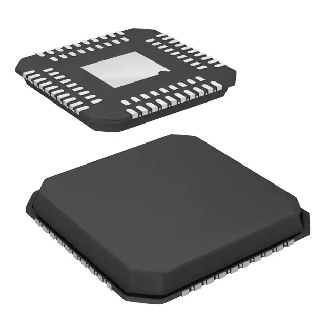


 工商网监
湘ICP备2023018690号
工商网监
湘ICP备2023018690号
