CC2652P
CC2652P
SWRS195B – OCTOBER 2019 – REVISED FEBRUARY
2021
SWRS195B – OCTOBER 2019 – REVISED FEBRUARY 2021
www.ti.com
CC2652P SimpleLink™ Multiprotocol 2.4 GHz Wireless MCU With Integrated Power
Amplifier
1 Features
•
•
•
•
•
•
Microcontroller
– Powerful 48-MHz Arm® Cortex®-M4F processor
– EEMBC CoreMark® score: 148
– 352KB of in-system programmable flash
– 256KB of ROM for protocols and library
functions
– 8KB of cache SRAM (alternatively available as
general-purpose RAM)
– 80KB of ultra-low leakage SRAM. The SRAM is
protected by parity to ensure high reliability of
operation.
– 2-pin cJTAG and JTAG debugging
– Supports over-the-air (OTA) update
Ultra-low power sensor controller with 4KB of
SRAM
– Sample, store, and process sensor data
– Operation independent from system CPU
– Fast wake-up for low-power operation
TI-RTOS, drivers, bootloader, Bluetooth® 5.2 low
energy controller, and IEEE 802.15.4 MAC in ROM
for optimized application size
RoHS-compliant package
– 7-mm × 7-mm RGZ VQFN48 (26 GPIOs)
Peripherals
– Digital peripherals can be routed to any GPIO
– 4× 32-bit or 8× 16-bit general-purpose timers
– 12-bit ADC, 200 kSamples/s, 8 channels
– 2× comparators with internal reference DAC
(1× continuous time, 1× ultra-low power)
– Programmable current source
– 2× UART
– 2× SSI (SPI, MICROWIRE, TI)
– I2C and I2S
– Real-time clock (RTC)
– AES 128- and 256-bit cryptographic accelerator
– ECC and RSA public key hardware accelerator
– SHA2 accelerator (full suite up to SHA-512)
– True random number generator (TRNG)
– Capacitive sensing, up to 8 channels
– Integrated temperature and battery monitor
External system
– On-chip buck DC/DC converter
•
•
•
•
Low power
– Active mode RX: 6.9 mA
– Active mode TX 0 dBm: 7.3 mA
– Active mode TX 5 dBm: 9.6 mA
– Active mode TX at +10 dBm: 22 mA
– Active mode TX at +20 dBm: 85 mA
– Active mode MCU 48 MHz (CoreMark):
3.4 mA (71 μA/MHz)
– Sensor controller, low power-mode, 2 MHz,
running infinite loop: 30.1 μA
– Sensor controller, active mode, 24 MHz,
running infinite loop: 808 μA
– Standby: 0.94 µA (RTC on, 80KB RAM and
CPU retention)
– Shutdown: 150 nA (wakeup on external events)
Radio section
– 2.4 GHz RF transceiver compatible with
Bluetooth 5.2 Low Energy and earlier LE
specifications and IEEE 802.15.4 PHY and
MAC
– 3-wire, 2-wire, 1-wire PTA coexistence
mechanisms
– Excellent receiver sensitivity:
-100 dBm for 802.15.4 (2.4 GHz),
-105 dBm for Bluetooth 125-kbps (LE Coded
PHY)
– Output power up to +20 dBm with temperature
compensation
– Suitable for systems targeting compliance with
worldwide radio frequency regulations
• EN 300 328, (Europe)
• EN 300 440 Category 2
• FCC CFR47 Part 15
• ARIB STD-T66 (Japan)
Wireless protocols
– Thread, Zigbee®, Bluetooth® 5.2 Low Energy,
IEEE 802.15.4, IPv6-enabled smart objects
(6LoWPAN), proprietary systems, SimpleLink™
TI 15.4 stack (2.4 GHz), and dynamic
multiprotocol manager (DMM) driver.
Development Tools and Software
– SimpleLink™ CC13x2 and CC26x2 Software
Development Kit (SDK)
– SmartRF™ Studio for simple radio configuration
– Sensor Controller Studio for building low-power
sensing applications
An©IMPORTANT
NOTICEIncorporated
at the end of this data sheet addresses availability, warranty, changes, use in
safety-critical
applications,
Copyright
2021 Texas Instruments
Submit
Document
Feedback
intellectual property matters and other important disclaimers. PRODUCTION DATA.
Product Folder Links: CC2652P
1
�CC2652P
www.ti.com
SWRS195B – OCTOBER 2019 – REVISED FEBRUARY 2021
2 Applications
•
•
•
2400 to 2480 MHz ISM and SRD systems 1
with down to 4 kHz of receive bandwidth
Building automation
– Building security systems – motion detector,
electronic smart lock, door and window sensor,
garage door system, gateway
– HVAC – thermostat, wireless environmental
sensor, HVAC system controller, gateway
– Fire safety system – smoke and heat detector,
fire alarm control panel (FACP)
– Video surveillance – IP network camera
– Elevators and escalators – elevator main
control panel for elevators and escalators
Grid infrastructure
– Smart meters – water meter, gas meter,
electricity meter, and heat cost allocators
– Grid communications – wireless
communications – Long-range sensor
applications
•
•
•
•
•
•
– Other alternative energy – energy harvesting
Industrial transport – asset tracking
Factory automation and control
Medical
Electronic point of sale (EPOS) – Electronic Shelf
Label (ESL)
Communication equipment
– Wired networking – wireless LAN or Wi-Fi
access points, edge router , small business
router
Personal electronics
– Portable electronics – RF smart remote control
– Home theater & entertainment – smart
speakers, smart display, set-top box
– Connected peripherals – consumer wireless
module, pointing devices, keyboards and
keypads
– Gaming – electronic and robotic toys
– Wearables (non-medical) – smart trackers,
smart clothing
3 Description
The SimpleLink™ CC2652P device is a multiprotocol 2.4 GHz wireless microcontroller (MCU) supporting Thread,
Zigbee®, Bluetooth® 5.2 Low Energy, IEEE 802.15.4, IPv6-enabled smart objects (6LoWPAN), proprietary
systems, including the TI 15.4-Stack (2.4 GHz), and concurrent multiprotocol through a Dynamic Multiprotocol
Manager (DMM) driver. The device is optimized for low-power wireless communication and advanced sensing in
building security systems, HVAC, medical, wired networking, portable electronics, home theater & entertainment,
and connected peripherals markets. The highlighted features of this device include:
• Wide flexibility of protocol stack support in the SimpleLink™ CC13x2 and CC26x2 Software Development Kit
(SDK).
• Enable long-range and low-power applications using integrated +20 dBm high-power amplifier with best-inclass transmit current consumption at 85 mA.
• Coin-cell operation at +10 dBm with transmit current consumption of 22 mA.
• Longer battery life wireless applications with low standby current of 0.94 µA with full RAM retention.
• Industrial temperature ready with lowest standby current of 5 µA at 85°C.
• Advanced sensing with a programmable, autonomous ultra-low power Sensor Controller CPU with fast wakeup capability. As an example, the sensor controller is capable of 1-Hz ADC sampling at 1 µA system current.
• Low SER (Soft Error Rate) FIT (Failure-in-time) for long operation lifetime with no disruption for industrial
markets with always-on SRAM parity against corruption due to potential radiation events.
• Dedicated software controlled radio controller (Arm® Cortex®-M0) providing flexible low-power RF transceiver
capability to support multiple physical layers and RF standards.
• Excellent radio sensitivity and robustness (selectivity and blocking) performance for Bluetooth ® Low Energy
(-105 dBm for 125-kbps LE Coded PHY).
The CC2652P device is part of the SimpleLink™ MCU platform, which consists of Wi-Fi®, Bluetooth Low Energy,
Thread, Zigbee, Sub-1 GHz MCUs, and host MCUs that all share a common, easy-to-use development
environment with a single core software development kit (SDK) and rich tool set. A one-time integration of the
SimpleLink™ platform enables you to add any combination of the portfolio’s devices into your design, allowing
100 percent code reuse when your design requirements change. For more information, visit SimpleLink™ MCU
platform.
1
2
See RF Core for additional details on supported protocol standards, modulation formats, and data rates.
Submit Document Feedback
Copyright © 2021 Texas Instruments Incorporated
Product Folder Links: CC2652P
�CC2652P
www.ti.com
SWRS195B – OCTOBER 2019 – REVISED FEBRUARY 2021
Device Information
PART NUMBER(1)
CC2652P1FRGZ
(1)
PACKAGE
BODY SIZE (NOM)
VQFN (48)
7.00 mm × 7.00 mm
For the most current part, package, and ordering information for all available devices, see the Package Option Addendum in Section
12, or see the TI website.
CC26x2P
z
G
H
2.
4
20
-d
B
m
PA
4 Functional Block Diagram
RF Core
cJTAG
Main CPU
256KB
ROM
ADC
ADC
Arm® Cortex®-M4F
Processor
Up to
352KB
Flash
with 8KB
Cache
48 MHz
69 µA/MHz
Up to
80KB
SRAM
Digital PLL
DSP Modem
Arm® Cortex®-M0
Processor
General Hardware Peripherals and Modules
I2C and I2S
16KB
SRAM
ROM
Sensor Interface
4× 32-bit Timers
ULP Sensor Controller
2× UART
2× SSI (SPI)
32 ch. µDMA
Watchdog Timer
26 GPIOs
TRNG
AES-256, SHA2-512
Temperature and
Battery Monitor
ECC, RSA
RTC
12-bit ADC, 200 ks/s
Low-Power Comparator
SPI-I2C Digital Sensor IF
Constant Current Source
Time-to-Digital Converter
LDO, Clocks, and References
Optional DC/DC Converter
4KB SRAM
Figure 4-1. CC2652P Block Diagram
Submit Document Feedback
Copyright © 2021 Texas Instruments Incorporated
Product Folder Links: CC2652P
3
�CC2652P
www.ti.com
SWRS195B – OCTOBER 2019 – REVISED FEBRUARY 2021
Table of Contents
1 Features............................................................................1
2 Applications..................................................................... 2
3 Description.......................................................................2
4 Functional Block Diagram.............................................. 3
5 Revision History.............................................................. 5
6 Device Comparison......................................................... 6
7 Terminal Configuration and Functions..........................7
7.1 Pin Diagram – RGZ Package (Top View)....................7
7.2 Signal Descriptions – RGZ Package...........................8
7.3 Connections for Unused Pins and Modules................9
8 Specifications................................................................ 10
8.1 Absolute Maximum Ratings ..................................... 10
8.2 ESD Ratings ............................................................ 10
8.3 Recommended Operating Conditions ......................10
8.4 Power Supply and Modules ..................................... 11
8.5 Power Consumption - Power Modes ....................... 12
8.6 Power Consumption - Radio Modes ........................ 13
8.7 Nonvolatile (Flash) Memory Characteristics ............ 13
8.8 Thermal Resistance Characteristics ........................ 13
8.9 RF Frequency Bands ............................................... 14
8.10 Bluetooth Low Energy - Receive (RX) ................... 15
8.11 Bluetooth Low Energy - Transmit (TX) ................... 18
8.12 Zigbee and Thread - IEEE 802.15.4-2006 2.4
GHz (OQPSK DSSS1:8, 250 kbps) - RX ................... 20
8.13 Zigbee and Thread - IEEE 802.15.4-2006 2.4
GHz (OQPSK DSSS1:8, 250 kbps) - TX ....................21
8.14 Timing and Switching Characteristics..................... 22
8.15 Peripheral Characteristics.......................................27
4
8.16 Typical Characteristics............................................ 35
9 Detailed Description......................................................54
9.1 Overview................................................................... 54
9.2 System CPU............................................................. 54
9.3 Radio (RF Core)........................................................55
9.4 Memory..................................................................... 55
9.5 Sensor Controller...................................................... 56
9.6 Cryptography............................................................ 58
9.7 Timers....................................................................... 59
9.8 Serial Peripherals and I/O.........................................60
9.9 Battery and Temperature Monitor............................. 60
9.10 µDMA...................................................................... 60
9.11 Debug......................................................................60
9.12 Power Management................................................61
9.13 Clock Systems........................................................ 62
9.14 Network Processor..................................................62
10 Application, Implementation, and Layout................. 63
10.1 Reference Designs................................................. 63
11 Device and Documentation Support..........................65
11.1 Tools and Software..................................................65
11.2 Documentation Support.......................................... 67
11.3 Support Resources................................................. 68
11.4 Trademarks............................................................. 68
11.5 Electrostatic Discharge Caution.............................. 68
11.6 Glossary.................................................................. 68
12 Mechanical, Packaging, and Orderable
Information.................................................................... 69
12.1 Packaging Information............................................ 69
Submit Document Feedback
Copyright © 2021 Texas Instruments Incorporated
Product Folder Links: CC2652P
�CC2652P
www.ti.com
SWRS195B – OCTOBER 2019 – REVISED FEBRUARY 2021
5 Revision History
NOTE: Page numbers for previous revisions may differ from page numbers in the current version.
Changes from April 24, 2020 to February 12, 2021 (from Revision A (April 2020) to Revision B
(February 2021))
Page
• Updated the numbering format for tables, figures, and cross-references throughout the document..................1
• Updated to Bluetooth 5.2 throughout the document........................................................................................... 1
• Added 3-wire, 2-wire, and 1-wire PTA coexistence mechanisms to the "Radio Section" list in Section 1
Features .............................................................................................................................................................1
• Removed Wi-SUN in the Wireless protocals list items in Section 1 Features ................................................... 1
• Changed the test condition to "Zero cycles" for the Flash sector erase time parameter in Section 8.7,
Nonvolatile (Flash) Memory Characteristics .................................................................................................... 10
• Changed the test condition to 85°C for the Flash retention parameter in Section 8.7, Nonvolatile (Flash)
Memory Characteristics ................................................................................................................................... 10
• Changed the frequency of the input tone for 14-bit and 15-bit mode in Section 8.15.1.1 ................................27
• Changed the test condition for the Accuracy parameter to 85°C in Section 8.15.3.1, Temperature Sensor ... 32
• Added PTA description in Section 9.3, Radio (RF Core) ................................................................................. 55
• Added information on SRAM parity ................................................................................................................. 55
• Added the paragraph that begins "Integrated matched filter-balun devices can be used…" in Section 10.1,
Reference Designs .......................................................................................................................................... 63
Submit Document Feedback
Copyright © 2021 Texas Instruments Incorporated
Product Folder Links: CC2652P
5
�CC2652P
www.ti.com
SWRS195B – OCTOBER 2019 – REVISED FEBRUARY 2021
6 Device Comparison
Table 6-1. Device Family Overview
RADIO SUPPORT
FLASH
(KB)
RAM
(KB)
GPIO
PACKAGE SIZE
CC1312R
Sub-1 GHz
352
80
30
RGZ (7-mm × 7-mm VQFN48)
CC1352P
Multiprotocol
Sub-1 GHz
Bluetooth 5.2 Low Energy
Zigbee
Thread
2.4 GHz proprietary FSK-based formats
+20-dBm high-power amplifier
352
80
26
RGZ (7-mm × 7-mm VQFN48)
CC1352R
Multiprotocol
Sub-1 GHz
Bluetooth 5.2 Low Energy
Zigbee
Thread
2.4 GHz proprietary FSK-based formats
352
80
28
RGZ (7-mm × 7-mm VQFN48)
CC2642R
Bluetooth 5.2 Low Energy
2.4 GHz proprietary FSK-based formats
352
80
31
RGZ (7-mm × 7-mm VQFN48)
CC2642R-Q1
Bluetooth 5.2 Low Energy
352
80
31
RTC (7-mm × 7-mm VQFN48)
CC2652R
Multiprotocol
Bluetooth 5.2 Low Energy
Zigbee
Thread
2.4 GHz proprietary FSK-based formats
352
80
31
RGZ (7-mm × 7-mm VQFN48)
CC2652RB
Multiprotocol
Bluetooth 5.2 Low Energy
Zigbee
Thread
2.4 GHz proprietary FSK-based formats
352
80
31
RGZ (7-mm × 7-mm VQFN48)
CC2652P
Multiprotocol
Bluetooth 5.2 Low Energy
Zigbee
Thread
2.4 GHz proprietary FSK-based formats
+19.5-dBm high-power amplifier
352
80
26
RGZ (7-mm × 7-mm VQFN48)
CC1310
Sub-1 GHz
32–128
16–20
10–31
RGZ (7-mm × 7-mm VQFN48)
RHB (5-mm × 5-mm VQFN32)
RSM (4-mm × 4-mm VQFN32)
CC1350
Sub-1 GHz
Bluetooth 4.2 Low Energy
128
20
10–31
RGZ (7-mm × 7-mm VQFN48)
RHB (5-mm × 5-mm VQFN32)
RSM (4-mm × 4-mm VQFN32)
CC2640R2F
Bluetooth 5.1 Low Energy
2.4 GHz proprietary FSK-based formats
128
20
10–31
RGZ (7-mm × 7-mm VQFN48)
RHB (5-mm × 5-mm VQFN32)
RSM (4-mm × 4-mm VQFN32)
YFV (2.7-mm × 2.7-mm DSBGA34)
CC2640R2F-Q1
Bluetooth 5.1 Low Energy
2.4 GHz proprietary FSK-based formats
128
20
31
RGZ (7-mm × 7-mm VQFN48)
DEVICE
6
Submit Document Feedback
Copyright © 2021 Texas Instruments Incorporated
Product Folder Links: CC2652P
�CC2652P
www.ti.com
SWRS195B – OCTOBER 2019 – REVISED FEBRUARY 2021
7 Terminal Configuration and Functions
38 DIO_25
37 DIO_24
40 DIO_27
39 DIO_26
42 DIO_29
41 DIO_28
44 VDDS
43 DIO_30
46 X48M_N
45 VDDR
48 VDDR_RF
47 X48M_P
7.1 Pin Diagram – RGZ Package (Top View)
RF_P
1
36 DIO_23
RF_N
2
35 RESET_N
NC
3
34 VDDS_DCDC
NC
TX_20DBM_P
4
33 DCDC_SW
5
32 DIO_22
TX_20DBM_N
6
31 DIO_21
RX_TX
7
30 DIO_20
X32K_Q1
8
29 DIO_19
X32K_Q2
DCOUPL 23
JTAG_TMSC 24
25 JTAG_TCKC
DIO_15 21
VDDS3 22
26 DIO_16
DIO_7 12
DIO_13 19
DIO_14 20
DIO_6 11
DIO_11 17
DIO_12 18
27 DIO_17
DIO_9 15
DIO_10 16
28 DIO_18
VDDS2 13
DIO_8 14
9
DIO_5 10
Figure 7-1. RGZ (7-mm × 7-mm) Pinout, 0.5-mm Pitch (Top View)
The following I/O pins marked in Figure 7-1 in bold have high-drive capabilities:
•
•
•
•
•
•
Pin 10, DIO_5
Pin 11, DIO_6
Pin 12, DIO_7
Pin 24, JTAG_TMSC
Pin 26, DIO_16
Pin 27, DIO_17
The following I/O pins marked in Figure 7-1 in italics have analog capabilities:
•
•
•
•
•
•
•
•
Pin 36, DIO_23
Pin 37, DIO_24
Pin 38, DIO_25
Pin 39, DIO_26
Pin 40, DIO_27
Pin 41, DIO_28
Pin 42, DIO_29
Pin 43, DIO_30
Submit Document Feedback
Copyright © 2021 Texas Instruments Incorporated
Product Folder Links: CC2652P
7
�CC2652P
www.ti.com
SWRS195B – OCTOBER 2019 – REVISED FEBRUARY 2021
7.2 Signal Descriptions – RGZ Package
Table 7-1. Signal Descriptions – RGZ Package
PIN
NAME
8
NO.
I/O
TYPE
DESCRIPTION
DCDC_SW
33
—
Power
Output from internal DC/DC converter(1)
DCOUPL
23
—
Power
For decoupling of internal 1.27 V regulated digital-supply (2)
DIO_5
10
I/O
Digital
GPIO, high-drive capability
DIO_6
11
I/O
Digital
GPIO, high-drive capability
DIO_7
12
I/O
Digital
GPIO, high-drive capability
DIO_8
14
I/O
Digital
GPIO
DIO_9
15
I/O
Digital
GPIO
DIO_10
16
I/O
Digital
GPIO
DIO_11
17
I/O
Digital
GPIO
DIO_12
18
I/O
Digital
GPIO
DIO_13
19
I/O
Digital
GPIO
DIO_14
20
I/O
Digital
GPIO
DIO_15
21
I/O
Digital
GPIO
DIO_16
26
I/O
Digital
GPIO, JTAG_TDO, high-drive capability
DIO_17
27
I/O
Digital
GPIO, JTAG_TDI, high-drive capability
DIO_18
28
I/O
Digital
GPIO
DIO_19
29
I/O
Digital
GPIO
DIO_20
30
I/O
Digital
GPIO
DIO_21
31
I/O
Digital
GPIO
DIO_22
32
I/O
Digital
GPIO
DIO_23
36
I/O
Digital or Analog
GPIO, analog capability
DIO_24
37
I/O
Digital or Analog
GPIO, analog capability
DIO_25
38
I/O
Digital or Analog
GPIO, analog capability
DIO_26
39
I/O
Digital or Analog
GPIO, analog capability
DIO_27
40
I/O
Digital or Analog
GPIO, analog capability
DIO_28
41
I/O
Digital or Analog
GPIO, analog capability
DIO_29
42
I/O
Digital or Analog
GPIO, analog capability
DIO_30
43
I/O
Digital or Analog
EGP
—
—
GND
Ground – exposed ground pad(3)
JTAG_TMSC
24
I/O
Digital
JTAG TMSC, high-drive capability
JTAG_TCKC
25
I
Digital
JTAG TCKC
RESET_N
35
I
Digital
Reset, active low. No internal pullup resistor
GPIO, analog capability
RF_P
1
—
RF
Positive RF input signal to LNA during RX
Positive RF output signal from PA during TX
RF_N
2
—
RF
Negative RF input signal to LNA during RX
Negative RF output signal from PA during TX
RX_TX
7
—
RF
Optional bias pin for the RF LNA
TX_20DBM_P
5
—
RF
Positive high-power TX signal
TX_20DBM_N
6
—
RF
Negative high-power TX signal
VDDR
45
—
Power
Internal supply, must be powered from the internal DC/DC
converter or the internal LDO(2) (4) (6)
VDDR_RF
48
—
Power
Internal supply, must be powered from the internal DC/DC
converter or the internal LDO(2) (5) (6)
VDDS
44
—
Power
1.8-V to 3.8-V main chip supply(1)
Submit Document Feedback
Copyright © 2021 Texas Instruments Incorporated
Product Folder Links: CC2652P
�CC2652P
www.ti.com
SWRS195B – OCTOBER 2019 – REVISED FEBRUARY 2021
Table 7-1. Signal Descriptions – RGZ Package (continued)
PIN
I/O
TYPE
13
—
Power
1.8-V to 3.8-V DIO supply(1)
VDDS3
22
—
Power
1.8-V to 3.8-V DIO supply(1)
VDDS_DCDC
34
—
Power
1.8-V to 3.8-V DC/DC converter supply
X48M_N
46
—
Analog
48-MHz crystal oscillator pin 1
X48M_P
47
—
Analog
48-MHz crystal oscillator pin 2
X32K_Q1
8
—
Analog
32-kHz crystal oscillator pin 1
X32K_Q2
9
—
Analog
32-kHz crystal oscillator pin 2
NAME
NO.
VDDS2
(1)
(2)
(3)
(4)
(5)
(6)
DESCRIPTION
For more details, see technical reference manual listed in Section 11.2.
Do not supply external circuitry from this pin.
EGP is the only ground connection for the device. Good electrical connection to device ground on printed circuit board (PCB) is
imperative for proper device operation.
If internal DC/DC converter is not used, this pin is supplied internally from the main LDO.
If internal DC/DC converter is not used, this pin must be connected to VDDR for supply from the main LDO.
Output from internal DC/DC and LDO is trimmed to 1.68 V.
7.3 Connections for Unused Pins and Modules
Table 7-2. Connections for Unused Pins
FUNCTION
GPIO
32.768-kHz crystal
No Connects
DC/DC converter(2)
(1)
(2)
SIGNAL NAME
DIO_n
PIN NUMBER
ACCEPTABLE PRACTICE(1)
PREFERRED
PRACTICE(1)
10–12
14–21
26–32
36–43
NC or GND
NC
NC or GND
NC
X32K_Q1
8
X32K_Q2
9
NC
3–4
NC
NC
DCDC_SW
33
NC
NC
VDDS_DCDC
34
VDDS
VDDS
NC = No connect
When the DC/DC converter is not used, the inductor between DCDC_SW and VDDR can be removed. VDDR and VDDR_RF must still
be connected and the 22 uF DCDC capacitor must be kept on the VDDR net.
Submit Document Feedback
Copyright © 2021 Texas Instruments Incorporated
Product Folder Links: CC2652P
9
�CC2652P
www.ti.com
SWRS195B – OCTOBER 2019 – REVISED FEBRUARY 2021
8 Specifications
8.1 Absolute Maximum Ratings
over operating free-air temperature range (unless otherwise noted)(1) (2)
MIN
VDDS(3)
–0.3
4.1
V
Voltage on any digital pin(4)
–0.3
VDDS + 0.3, max 4.1
V
Voltage on crystal oscillator pins, X32K_Q1, X32K_Q2, X48M_N and X48M_P
–0.3
VDDR + 0.3, max 2.25
V
–0.3
VDDS
Voltage on ADC input
Voltage scaling disabled, internal reference
–0.3
1.49
Voltage scaling disabled, VDDS as reference
–0.3
VDDS / 2.9
–40
150
Input level, RF pins
Tstg
(1)
(2)
(3)
(4)
UNIT
Supply voltage
Voltage scaling enabled
Vin
MAX
5
Storage temperature
V
dBm
°C
Stresses beyond those listed under Absolute Maximum Ratings may cause permanent damage to the device. These are stress ratings
only, and functional operation of the device at these or any other conditions beyond those indicated under Recommended Operating
Conditions is not implied. Exposure to absolute-maximum-rated conditions for extended periods may affect device reliability.
All voltage values are with respect to ground, unless otherwise noted.
VDDS_DCDC, VDDS2 and VDDS3 must be at the same potential as VDDS.
Including analog capable DIOs.
8.2 ESD Ratings
VESD
(1)
(2)
Electrostatic
discharge
Human body model (HBM), per ANSI/ESDA/JEDEC
JS001(1)
Charged device model (CDM), per JESD22-C101(2)
VALUE
UNIT
All pins
±2000
V
All pins
±500
V
JEDEC document JEP155 states that 500-V HBM allows safe manufacturing with a standard ESD control process.
JEDEC document JEP157 states that 250-V CDM allows safe manufacturing with a standard ESD control process.
8.3 Recommended Operating Conditions
over operating free-air temperature range (unless otherwise noted)
MIN
MAX
Operating ambient temperature
–40
85
Operating supply voltage (VDDS)
UNIT
°C
1.8
3.8
V
Rising supply voltage slew rate
0
100
mV/µs
Falling supply voltage slew rate(1)
0
20
mV/µs
(1)
10
For small coin-cell batteries, with high worst-case end-of-life equivalent source resistance, a 22-µF VDDS input capacitor must be used
to ensure compliance with this slew rate.
Submit Document Feedback
Copyright © 2021 Texas Instruments Incorporated
Product Folder Links: CC2652P
�CC2652P
www.ti.com
SWRS195B – OCTOBER 2019 – REVISED FEBRUARY 2021
8.4 Power Supply and Modules
over operating free-air temperature range (unless otherwise noted)
PARAMETER
MIN
VDDS Brown-out Detector (BOD), before initial boot
VDDS Brown-out Detector (BOD) (1)
(1)
(2)
(2)
MAX
UNIT
V
Rising threshold
1.77
V
Rising threshold
1.70
V
Falling threshold
1.75
V
VDDS Power-on-Reset (POR) threshold
VDDS Brown-out Detector (BOD) (1)
TYP
1.1 1.55
For boost mode (VDDR =1.95 V), TI drivers software initialization will trim VDDS BOD limits to maximum (approximately 2.0 V)
Brown-out Detector is trimmed at initial boot, value is kept until device is reset by a POR reset or the RESET_N pin
Submit Document Feedback
Copyright © 2021 Texas Instruments Incorporated
Product Folder Links: CC2652P
11
�CC2652P
www.ti.com
SWRS195B – OCTOBER 2019 – REVISED FEBRUARY 2021
8.5 Power Consumption - Power Modes
When measured on the CC1352PEM-XD7793-XD24-PA24 reference design with Tc = 25 °C, VDDS = 3.0 V with DC/DC
enabled unless otherwise noted.
PARAMETER
TEST CONDITIONS
TYP
UNIT
Core Current Consumption
Reset. RESET_N pin asserted or VDDS below power-on-reset
Reset and Shutdown threshold
Shutdown. No clocks running, no retention
150
nA
150
RTC running, CPU, 80KB RAM and (partial) register retention.
RCOSC_LF
0.94
µA
RTC running, CPU, 80KB RAM and (partial) register retention
XOSC_LF
1.09
µA
RTC running, CPU, 80KB RAM and (partial) register retention.
RCOSC_LF
3.2
µA
RTC running, CPU, 80KB RAM and (partial) register retention.
XOSC_LF
3.3
µA
Idle
Supply Systems and RAM powered
RCOSC_HF
675
µA
Active
MCU running CoreMark at 48 MHz
RCOSC_HF
3.39
mA
Standby
without cache
retention
Icore
Standby
with cache retention
Peripheral Current Consumption(1) (2)
Peripheral power
domain
Delta current with domain enabled
97.7
Serial power domain Delta current with domain enabled
7.2
RF Core
Iperi
Delta current with power domain enabled,
clock enabled, RF core idle
210.9
µDMA
Delta current with clock enabled, module is idle
63.9
Timers
Delta current with clock enabled, module is idle(5)
81.0
I2C
Delta current with clock enabled, module is idle
10.1
I2S
Delta current with clock enabled, module is idle
26.3
SSI
Delta current with clock enabled, module is idle
UART
Delta current with clock enabled, module is idle(3)
167.5
CRYPTO (AES)
Delta current with clock enabled, module is idle(4)
25.6
PKA
Delta current with clock enabled, module is idle
84.7
TRNG
Delta current with clock enabled, module is idle
35.6
µA
82.9
Sensor Controller Engine Consumption
ISCE
(1)
(2)
(3)
(4)
(5)
12
Active mode
24 MHz, infinite loop
808.5
Low-power mode
2 MHz, infinite loop
30.1
µA
Adds to core current Icore for each peripheral unit activated.
Iperi is not supported in Standby or Shutdown modes.
Only one UART running
Only one SSI running
Only one GPTimer running
Submit Document Feedback
Copyright © 2021 Texas Instruments Incorporated
Product Folder Links: CC2652P
�CC2652P
www.ti.com
SWRS195B – OCTOBER 2019 – REVISED FEBRUARY 2021
8.6 Power Consumption - Radio Modes
When measured on the CC1352PEM-XD7793-XD24-PA24 reference design with Tc = 25 °C, VDDS = 3.0 V with DC/DC
enabled unless otherwise noted.
High-power PA connected to VDDS unless otherwise noted.
PARAMETER
TEST CONDITIONS
TYP
UNIT
2440 MHz
6.9
mA
0 dBm output power setting
2440 MHz
7.3
mA
+5 dBm output power setting
2440 MHz
9.6
mA
Radio transmit current
High-power PA
+20 dBm output power setting
2440 MHz. VDDS = 3.3 V
85
mA
Radio transmit current
High-power PA, 10 dBm
configuration(1)
+10 dBm output power setting
2440 MHz VDDR = 1.67 V
22
mA
Radio receive current
Radio transmit current
2.4 GHz PA (BLE)
(1)
Measured on evaluation board as described in Optimizing the CC1352P and CC2652P for Coin Cell Operation at 10 dBm Output
Power.
8.7 Nonvolatile (Flash) Memory Characteristics
Over operating free-air temperature range and VDDS = 3.0 V (unless otherwise noted)
PARAMETER
TEST CONDITIONS
MIN
TYP
Flash sector size
Supported flash erase cycles before failure, full
(5)
bank(1)
Supported flash erase cycles before failure, single
sector(2)
KB
k Cycles
60
k Cycles
83
Flash retention
85 °C
Flash sector erase current
Write
Operations
Years at
85 °C
11.4
Average delta current
time(4)
UNIT
30
Maximum number of write operations per row before
sector erase(3)
Flash sector erase
MAX
8
10.7
mA
Zero cycles
10
ms
Flash write current
Average delta current, 4 bytes at a time
6.2
mA
Flash write time(4)
4 bytes at a time
21.6
µs
(1)
(2)
(3)
(4)
(5)
A full bank erase is counted as a single erase cycle on each sector
Up to 4 customer-designated sectors can be individually erased an additional 30k times beyond the baseline bank limitation of 30k
cycles
Each wordline is 2048 bits (or 256 bytes) wide. This limitation corresponds to sequential memory writes of 4 (3.1) bytes minimum per
write over a whole wordline. If additional writes to the same wordline are required, a sector erase is required once the maximum
number of write operations per row is reached.
This number is dependent on Flash aging and increases over time and erase cycles
Aborting flash during erase or program modes is not a safe operation.
8.8 Thermal Resistance Characteristics
PACKAGE
THERMAL METRIC(1)
RGZ
(VQFN)
UNIT
48 PINS
RθJA
Junction-to-ambient thermal resistance
23.4
°C/W(2)
RθJC(top)
Junction-to-case (top) thermal resistance
13.3
°C/W(2)
RθJB
Junction-to-board thermal resistance
8.0
°C/W(2)
Submit Document Feedback
Copyright © 2021 Texas Instruments Incorporated
Product Folder Links: CC2652P
13
�CC2652P
www.ti.com
SWRS195B – OCTOBER 2019 – REVISED FEBRUARY 2021
8.8 Thermal Resistance Characteristics (continued)
PACKAGE
THERMAL METRIC(1)
RGZ
(VQFN)
UNIT
48 PINS
ψJT
Junction-to-top characterization parameter
0.1
°C/W(2)
ψJB
Junction-to-board characterization parameter
7.9
°C/W(2)
RθJC(bot)
Junction-to-case (bottom) thermal resistance
1.7
°C/W(2)
(1)
(2)
For more information about traditional and new thermal metrics, see Semiconductor and IC Package Thermal Metrics.
°C/W = degrees Celsius per watt.
8.9 RF Frequency Bands
Over operating free-air temperature range (unless otherwise noted).
PARAMETER
MIN
Frequency bands
14
2360
Submit Document Feedback
TYP
MAX
UNIT
2500
MHz
Copyright © 2021 Texas Instruments Incorporated
Product Folder Links: CC2652P
�CC2652P
www.ti.com
SWRS195B – OCTOBER 2019 – REVISED FEBRUARY 2021
8.10 Bluetooth Low Energy - Receive (RX)
Measured on the CC1352PEM-XD7793-XD24-PA24 reference design with Tc = 25 °C, VDDS = 3.0 V, fRF= 2440 MHz with
DC/DC enabled and high power PA connected to VDDS unless otherwise noted.
All measurements are performed at the antenna input with a combined RX and TX path, except for high power PA which is
measured at a dedicated antenna connection. All measurements are performed conducted.
PARAMETER
TEST CONDITIONS
MIN
TYP
MAX
UNIT
125 kbps (LE Coded)
Receiver sensitivity
Differential mode. BER = 10–3
–105
dBm
Receiver saturation
Differential mode. BER = 10–3
>5
dBm
Frequency error tolerance
Difference between the incoming carrier
frequency and the internally generated carrier
frequency
> (–300 / 300)
kHz
Data rate error tolerance
Difference between incoming data rate and the
internally generated data rate (37-byte packets)
> (–320 / 240)
ppm
Data rate error tolerance
Difference between incoming data rate and the
internally generated data rate (255-byte packets)
> (–125 / 125)
ppm
Co-channel rejection(1)
Wanted signal at –79 dBm, modulated interferer in
channel, BER = 10–3
–1.5
dB
Selectivity, ±1 MHz(1)
Wanted signal at –79 dBm, modulated interferer at
±1 MHz, BER = 10–3
8 / 4.5(2)
dB
Selectivity, ±2 MHz(1)
Wanted signal at –79 dBm, modulated interferer at
±2 MHz, BER = 10–3
44 / 39 (2)
dB
Selectivity, ±3 MHz(1)
Wanted signal at –79 dBm, modulated interferer at
±3 MHz, BER = 10–3
46 / 44(2)
dB
Selectivity, ±4 MHz(1)
Wanted signal at –79 dBm, modulated interferer at
±4 MHz, BER = 10–3
44 / 46(2)
dB
Selectivity, ±6 MHz(1)
Wanted signal at –79 dBm, modulated interferer at
≥ ±6 MHz, BER = 10–3
48 / 44(2)
dB
Selectivity, ±7 MHz
Wanted signal at –79 dBm, modulated interferer at
≥ ±7 MHz, BER = 10–3
51 / 45(2)
dB
Selectivity, Image frequency(1)
Wanted signal at –79 dBm, modulated interferer at
image frequency, BER = 10–3
Selectivity, Image frequency ±1
MHz(1)
Note that Image frequency + 1 MHz is the Cochannel –1 MHz. Wanted signal at –79 dBm,
modulated interferer at ±1 MHz from image
frequency, BER = 10–3
dB
4.5 / 44 (2)
dB
500 kbps (LE Coded)
Receiver sensitivity
Differential mode. BER = 10–3
–100
dBm
Receiver saturation
Differential mode. BER = 10–3
>5
dBm
Frequency error tolerance
Difference between the incoming carrier
frequency and the internally generated carrier
frequency
> (–300 / 300)
kHz
Data rate error tolerance
Difference between incoming data rate and the
internally generated data rate (37-byte packets)
> (–450 / 450)
ppm
Data rate error tolerance
Difference between incoming data rate and the
internally generated data rate (255-byte packets)
> ( –175 / 175)
ppm
Co-channel rejection(1)
Wanted signal at –72 dBm, modulated interferer in
channel, BER = 10–3
–3.5
dB
Selectivity, ±1 MHz(1)
Wanted signal at –72 dBm, modulated interferer at
±1 MHz, BER = 10–3
8 / 4(2)
dB
Selectivity, ±2 MHz(1)
Wanted signal at –72 dBm, modulated interferer at
±2 MHz, BER = 10–3
44 / 37 (2)
dB
Selectivity, ±3 MHz(1)
Wanted signal at –72 dBm, modulated interferer at
±3 MHz, BER = 10–3
46 / 46(2)
dB
Submit Document Feedback
Copyright © 2021 Texas Instruments Incorporated
Product Folder Links: CC2652P
15
�CC2652P
www.ti.com
SWRS195B – OCTOBER 2019 – REVISED FEBRUARY 2021
8.10 Bluetooth Low Energy - Receive (RX) (continued)
Measured on the CC1352PEM-XD7793-XD24-PA24 reference design with Tc = 25 °C, VDDS = 3.0 V, fRF= 2440 MHz with
DC/DC enabled and high power PA connected to VDDS unless otherwise noted.
All measurements are performed at the antenna input with a combined RX and TX path, except for high power PA which is
measured at a dedicated antenna connection. All measurements are performed conducted.
PARAMETER
TEST CONDITIONS
MIN
TYP
MAX
UNIT
Selectivity, ±4 MHz(1)
Wanted signal at –72 dBm, modulated interferer at
±4 MHz, BER = 10–3
45 / 47(2)
dB
Selectivity, ±6 MHz(1)
Wanted signal at –72 dBm, modulated interferer at
≥ ±6 MHz, BER = 10–3
46 / 45(2)
dB
Selectivity, ±7 MHz
Wanted signal at –72 dBm, modulated interferer at
≥ ±7 MHz, BER = 10–3
49 / 45(2)
dB
Selectivity, Image frequency(1)
Wanted signal at –72 dBm, modulated interferer at
image frequency, BER = 10–3
Selectivity, Image frequency ±1
MHz(1)
Note that Image frequency + 1 MHz is the Cochannel –1 MHz. Wanted signal at –72 dBm,
modulated interferer at ±1 MHz from image
frequency, BER = 10–3
dB
4 / 46(2)
dB
1 Mbps (LE 1M)
Receiver sensitivity
Differential mode. BER = 10–3
–97
dBm
Receiver saturation
Differential mode. BER = 10–3
>5
dBm
Frequency error tolerance
Difference between the incoming carrier
frequency and the internally generated carrier
frequency
> (–350 / 350)
kHz
Data rate error tolerance
Difference between incoming data rate and the
internally generated data rate (37-byte packets)
> ( –750 / 750)
ppm
Co-channel rejection(1)
Wanted signal at –67 dBm, modulated interferer in
channel, BER = 10–3
–6
dB
Selectivity, ±1 MHz(1)
Wanted signal at –67 dBm, modulated interferer at
±1 MHz, BER = 10–3
7 / 4(2)
dB
Selectivity, ±2 MHz(1)
Wanted signal at –67 dBm, modulated interferer at
±2 MHz,BER = 10–3
40 / 33(2)
dB
Selectivity, ±3 MHz(1)
Wanted signal at –67 dBm, modulated interferer at
±3 MHz, BER = 10–3
36 / 41 (2)
dB
Selectivity, ±4 MHz(1)
Wanted signal at –67 dBm, modulated interferer at
±4 MHz, BER = 10–3
36 / 45(2)
dB
Selectivity, ±5 MHz or more(1)
Wanted signal at –67 dBm, modulated interferer at
≥ ±5 MHz, BER = 10–3
40
dB
Selectivity, image frequency(1)
Wanted signal at –67 dBm, modulated interferer at
image frequency, BER = 10–3
33
dB
Selectivity, image frequency
±1 MHz(1)
Note that Image frequency + 1 MHz is the Cochannel –1 MHz. Wanted signal at –67 dBm,
modulated interferer at ±1 MHz from image
frequency, BER = 10–3
4 / 41(2)
dB
Out-of-band blocking(3)
30 MHz to 2000 MHz
–10
dBm
Out-of-band blocking
2003 MHz to 2399 MHz
–18
dBm
Out-of-band blocking
2484 MHz to 2997 MHz
–12
dBm
Out-of-band blocking
3000 MHz to 12.75 GHz
–2
dBm
Intermodulation
Wanted signal at 2402 MHz, –64 dBm. Two
interferers at 2405 and 2408 MHz respectively, at
the given power level
–42
dBm
Spurious emissions,
30 to 1000 MHz(4)
Measurement in a 50-Ω single-ended load.
< –59
dBm
Spurious emissions,
1 to 12.75 GHz(4)
Measurement in a 50-Ω single-ended load.
< –47
dBm
16
Submit Document Feedback
Copyright © 2021 Texas Instruments Incorporated
Product Folder Links: CC2652P
�CC2652P
www.ti.com
SWRS195B – OCTOBER 2019 – REVISED FEBRUARY 2021
8.10 Bluetooth Low Energy - Receive (RX) (continued)
Measured on the CC1352PEM-XD7793-XD24-PA24 reference design with Tc = 25 °C, VDDS = 3.0 V, fRF= 2440 MHz with
DC/DC enabled and high power PA connected to VDDS unless otherwise noted.
All measurements are performed at the antenna input with a combined RX and TX path, except for high power PA which is
measured at a dedicated antenna connection. All measurements are performed conducted.
PARAMETER
TEST CONDITIONS
MIN
TYP
MAX
UNIT
RSSI dynamic range
70
dB
RSSI accuracy
±4
dB
2 Mbps (LE 2M)
Receiver sensitivity
Differential mode. Measured at SMA connector,
BER = 10–3
–92
dBm
Receiver saturation
Differential mode. Measured at SMA connector,
BER = 10–3
>5
dBm
Frequency error tolerance
Difference between the incoming carrier
frequency and the internally generated carrier
frequency
> (–500 / 500)
kHz
Data rate error tolerance
Difference between incoming data rate and the
internally generated data rate (37-byte packets)
> (–700 / 750)
ppm
Co-channel rejection(1)
Wanted signal at –67 dBm, modulated interferer in
channel,BER = 10–3
–7
dB
Selectivity, ±2 MHz(1)
Wanted signal at –67 dBm, modulated interferer at
±2 MHz, Image frequency is at –2 MHz, BER =
10–3
8 / 4(2)
dB
Selectivity, ±4 MHz(1)
Wanted signal at –67 dBm, modulated interferer at
±4 MHz, BER = 10–3
36 / 36 (2)
dB
Selectivity, ±6 MHz(1)
Wanted signal at –67 dBm, modulated interferer at
±6 MHz, BER = 10–3
37 / 36(2)
dB
Selectivity, image frequency(1)
Wanted signal at –67 dBm, modulated interferer at
image frequency, BER = 10–3
4
dB
Selectivity, image frequency
±2 MHz(1)
Note that Image frequency + 2 MHz is the Cochannel. Wanted signal at –67 dBm, modulated
interferer at ±2 MHz from image frequency, BER =
10–3
–7 / 36(2)
dB
Out-of-band blocking(3)
30 MHz to 2000 MHz
–16
dBm
Out-of-band blocking
2003 MHz to 2399 MHz
–21
dBm
Out-of-band blocking
2484 MHz to 2997 MHz
–15
dBm
Out-of-band blocking
3000 MHz to 12.75 GHz
–12
dBm
Intermodulation
Wanted signal at 2402 MHz, –64 dBm. Two
interferers at 2408 and 2414 MHz respectively, at
the given power level
–38
dBm
(1)
(2)
(3)
(4)
Numbers given as I/C dB
X / Y, where X is +N MHz and Y is –N MHz
Excluding one exception at Fwanted / 2, per Bluetooth Specification
Suitable for systems targeting compliance with worldwide radio-frequency regulations ETSI EN 300 328 and EN 300 440 Class 2
(Europe), FCC CFR47 Part 15 (US), and ARIB STD-T66 (Japan)
Submit Document Feedback
Copyright © 2021 Texas Instruments Incorporated
Product Folder Links: CC2652P
17
�CC2652P
www.ti.com
SWRS195B – OCTOBER 2019 – REVISED FEBRUARY 2021
8.11 Bluetooth Low Energy - Transmit (TX)
Measured on the CC1352PEM-XD7793-XD24-PA24 reference design with Tc = 25 °C, VDDS = 3.0 V, fRF= 2440 MHz with
DC/DC enabled and high power PA connected to VDDS unless otherwise noted.
All measurements are performed at the antenna input with a combined RX and TX path, except for high power PA which is
measured at a dedicated antenna connection. All measurements are performed conducted.
PARAMETER
TEST CONDITIONS
MIN
TYP
MAX UNIT
dBm
General Parameters
Max output power,
high power PA
Differential mode, delivered to a single-ended 50 Ω load through a balun
19.5
Output power
programmable
range
high power PA
Differential mode, delivered to a single-ended 50 Ω load through a balun
6
Max output power,
high power PA, 10
Differential mode, delivered to a single-ended 50 Ω load through a balun
dBm configuration(4)
10.5
Output power
programmable
Differential mode, delivered to a single-ended 50 Ω load through a balun
range
high power PA, 10
dBm configuration(4)
5
dB
Max output power,
regular PA
Differential mode, delivered to a single-ended 50 Ω load through a balun
5
dBm
Output power
programmable
range,
regular PA
Differential mode, delivered to a single-ended 50 Ω load through a balun
26
dB
dB
dBm
Spurious emissions and harmonics
f < 1 GHz, outside restricted
bands
< -36
dBm
< -55
dBm
f > 1 GHz, including harmonics
-37
dBm
Second harmonic
-35
dBm
Third harmonic
-42
dBm
< -36
dBm
< -54
dBm
< -55
dBm
Spurious emissions,
f < 1 GHz, restricted bands
high-power PA(1) (2)
FCC
Harmonics,
high-power PA(1) (3)
+20 dBm setting
f < 1 GHz, outside restricted
bands
Spurious emissions, f < 1 GHz, restricted bands
high-power PA, 10 ETSI
dBm configuration(1)
(2) (4)
f < 1 GHz, restricted bands
FCC
+10 dBm setting(4)
f > 1 GHz, including harmonics
Harmonics,
Second harmonic
high-power PA, 10
dBm configuration(1) Third harmonic
(4)
18
Submit Document Feedback
-41
dBm
< -42
dBm
< -42
dBm
Copyright © 2021 Texas Instruments Incorporated
Product Folder Links: CC2652P
�CC2652P
www.ti.com
SWRS195B – OCTOBER 2019 – REVISED FEBRUARY 2021
8.11 Bluetooth Low Energy - Transmit (TX) (continued)
Measured on the CC1352PEM-XD7793-XD24-PA24 reference design with Tc = 25 °C, VDDS = 3.0 V, fRF= 2440 MHz with
DC/DC enabled and high power PA connected to VDDS unless otherwise noted.
All measurements are performed at the antenna input with a combined RX and TX path, except for high power PA which is
measured at a dedicated antenna connection. All measurements are performed conducted.
PARAMETER
TEST CONDITIONS
TYP
MAX UNIT
< –36
dBm
< –54
dBm
< –55
dBm
f > 1 GHz, including harmonics
< –42
dBm
Second harmonic
< –42
dBm
Third harmonic
< –42
dBm
f < 1 GHz, outside restricted
bands
f < 1 GHz, restricted bands
Spurious emissions, ETSI
regular PA (1)
f < 1 GHz, restricted bands
FCC
Harmonics,
regular PA (1)
(1)
(2)
(3)
(4)
+5 dBm setting
MIN
Suitable for systems targeting compliance with worldwide radio-frequency regulations ETSI EN 300 328 and EN 300 440 Class 2
(Europe), FCC CFR47 Part 15 (US), and ARIB STD-T66 (Japan).
To ensure margins for passing FCC band edge requirements at 2483.5 MHz, a lower than maximum output-power setting or less than
100% duty cycle may be used when operating at the upper BLE channel(s).
To ensure margins for passing FCC requirements for harmonic emission, duty cycling may be required. The CC1352P-2 LaunchPad
reference design should also be reviewed as the filter provides higher attenuation of harmonics compared to the CC1352PEMXD7793-XD24-PA24 reference design.
Measured on evaluation board as described in Optimizing the CC1352P and CC2652P for Coin Cell Operation at 10 dBm Output
Power.
Submit Document Feedback
Copyright © 2021 Texas Instruments Incorporated
Product Folder Links: CC2652P
19
�CC2652P
www.ti.com
SWRS195B – OCTOBER 2019 – REVISED FEBRUARY 2021
8.12 Zigbee and Thread - IEEE 802.15.4-2006 2.4 GHz (OQPSK DSSS1:8, 250 kbps) - RX
Measured on the CC1352PEM-XD7793-XD24-PA24 reference design with Tc = 25 °C, VDDS = 3.0 V, fRF= 2440 MHz with
DC/DC enabled and high power PA connected to VDDS unless otherwise noted.
All measurements are performed at the antenna input with a combined RX and TX path, except for high power PA which is
measured at a dedicated antenna connection. All measurements are performed conducted.
PARAMETER
TEST CONDITIONS
MIN
TYP
MAX
UNIT
General Parameters
Receiver sensitivity
PER = 1%
–100
dBm
Receiver saturation
PER = 1%
>5
dBm
Adjacent channel rejection
Wanted signal at –82 dBm, modulated interferer at
±5 MHz, PER = 1%
36
dB
Alternate channel rejection
Wanted signal at –82 dBm, modulated interferer at
±10 MHz, PER = 1%
57
dB
Channel rejection, ±15 MHz or
more
Wanted signal at –82 dBm, undesired signal is IEEE
802.15.4 modulated channel, stepped through all
channels 2405 to 2480 MHz, PER = 1%
59
dB
Blocking and desensitization,
5 MHz from upper band edge
Wanted signal at –97 dBm (3 dB above the
sensitivity level), CW jammer, PER = 1%
57
dB
Blocking and desensitization,
10 MHz from upper band edge
Wanted signal at –97 dBm (3 dB above the
sensitivity level), CW jammer, PER = 1%
63
dB
Blocking and desensitization,
20 MHz from upper band edge
Wanted signal at –97 dBm (3 dB above the
sensitivity level), CW jammer, PER = 1%
63
dB
Blocking and desensitization,
50 MHz from upper band edge
Wanted signal at –97 dBm (3 dB above the
sensitivity level), CW jammer, PER = 1%
66
dB
Blocking and desensitization,
–5 MHz from lower band edge
Wanted signal at –97 dBm (3 dB above the
sensitivity level), CW jammer, PER = 1%
60
dB
Blocking and desensitization,
–10 MHz from lower band edge
Wanted signal at –97 dBm (3 dB above the
sensitivity level), CW jammer, PER = 1%
60
dB
Blocking and desensitization,
–20 MHz from lower band edge
Wanted signal at –97 dBm (3 dB above the
sensitivity level), CW jammer, PER = 1%
63
dB
Blocking and desensitization,
–50 MHz from lower band edge
Wanted signal at –97 dBm (3 dB above the
sensitivity level), CW jammer, PER = 1%
65
dB
Spurious emissions, 30 MHz to
1000 MHz(1)
Measurement in a 50-Ω single-ended load
–66
dBm
Spurious emissions, 1 GHz to
12.75 GHz(1)
Measurement in a 50-Ω single-ended load
–53
dBm
Frequency error tolerance
Difference between the incoming carrier frequency
and the internally generated carrier frequency
> 350
ppm
Symbol rate error tolerance
Difference between incoming symbol rate and the
internally generated symbol rate
> 1000
ppm
RSSI dynamic range
95
dB
RSSI accuracy
±4
dB
(1)
20
Suitable for systems targeting compliance with worldwide radio-frequency regulations ETSI EN 300 328 and EN 300 440 Class 2
(Europe), FCC CFR47 Part 15 (US), and ARIB STD-T66 (Japan)
Submit Document Feedback
Copyright © 2021 Texas Instruments Incorporated
Product Folder Links: CC2652P
�CC2652P
www.ti.com
SWRS195B – OCTOBER 2019 – REVISED FEBRUARY 2021
8.13 Zigbee and Thread - IEEE 802.15.4-2006 2.4 GHz (OQPSK DSSS1:8, 250 kbps) - TX
Measured on the CC1352PEM-XD7793-XD24-PA24 reference design with Tc = 25 °C, VDDS = 3.0 V, fRF= 2440 MHz with
DC/DC enabled and high power PA connected to VDDS unless otherwise noted.
All measurements are performed at the antenna input with a combined RX and TX path, except for high power PA which is
measured at a dedicated antenna connection. All measurements are performed conducted.
PARAMETER
TEST CONDITIONS
MIN
TYP
MAX UNIT
dBm
General Parameters
Max output power,
high power PA
Differential mode, delivered to a single-ended 50-Ω load through a balun
19.5
Output power
programmable range,
high power PA
Differential mode, delivered to a single-ended 50-Ω load through a balun
6
Max output power,
high power PA, 10
dBm configuration(5)
Differential mode, delivered to a single-ended 50-Ω load through a balun
10.5
Output power
programmable range,
high power PA, 10
dBm configuration(5)
Differential mode, delivered to a single-ended 50-Ω load through a balun
5
dB
Max output power,
regular PA
Differential mode, delivered to a single-ended 50-Ω load through a balun
5
dBm
Output power
programmable range,
regular PA
Differential mode, delivered to a single-ended 50-Ω load through a balun
26
dB
dB
dBm
Spurious emissions and harmonics
f < 1 GHz, outside restricted
bands
Spurious emissions,
high-power PA(1) (3)
< -39
dBm
< -49
dBm
-40
dBm
Second harmonic
-35
dBm
Third harmonic
f < 1 GHz, restricted bands
FCC
f > 1 GHz, including
harmonics
Harmonics,
high-power PA(1) (4)
Spurious emissions,
high-power PA, 10
dBm configuration(1)
(3) (5)
+20 dBm setting
-42
dBm
f < 1 GHz, outside restricted
bands
< -36
dBm
f < 1 GHz, restricted bands
ETSI
< -47
dBm
< -55
dBm
-42
dBm
Second harmonic
< -42
dBm
Third harmonic
< -42
dBm
f < 1 GHz, outside restricted
bands
< -36
dBm
f < 1 GHz, restricted bands
ETSI
< -47
dBm
< -55
dBm
f > 1 GHz, including
harmonics
< –42
dBm
Second harmonic
< -42
dBm
Third harmonic
< -42
dBm
f < 1 GHz, restricted bands
FCC
+10 dBm setting(5)
f > 1 GHz, including
harmonics
Harmonics,
high-power PA, 10
dBm configuration(1)
(5)
Spurious emissions,
regular PA (1) (2)
Harmonics,
regular PA (1)
f < 1 GHz, restricted bands
FCC
+5 dBm setting
Submit Document Feedback
Copyright © 2021 Texas Instruments Incorporated
Product Folder Links: CC2652P
21
�CC2652P
www.ti.com
SWRS195B – OCTOBER 2019 – REVISED FEBRUARY 2021
8.13 Zigbee and Thread - IEEE 802.15.4-2006 2.4 GHz (OQPSK DSSS1:8, 250 kbps) - TX
(continued)
Measured on the CC1352PEM-XD7793-XD24-PA24 reference design with Tc = 25 °C, VDDS = 3.0 V, fRF= 2440 MHz with
DC/DC enabled and high power PA connected to VDDS unless otherwise noted.
All measurements are performed at the antenna input with a combined RX and TX path, except for high power PA which is
measured at a dedicated antenna connection. All measurements are performed conducted.
PARAMETER
TEST CONDITIONS
MIN
TYP
MAX UNIT
IEEE 802.15.4-2006 2.4 GHz (OQPSK DSSS1:8, 250 kbps)
Error vector
magnitude,
high power PA
+20 dBm setting
2
%
Error vector
magnitude,
high power PA, 10
dBm configuration(5)
+10 dBm setting
2
%
Error vector
magnitude
Regular PA
+5 dBm setting
2
%
(1)
(2)
(3)
(4)
(5)
Suitable for systems targeting compliance with worldwide radio-frequency regulations ETSI EN 300 328 and EN 300 440 Class 2
(Europe), FCC CFR47 Part 15 (US), and ARIB STD-T66 (Japan).
To ensure margins for passing FCC band edge requirements at 2483.5 MHz, a lower than maximum output-power setting or less than
100% duty cycle may be used when operating at 2480 MHz.
To ensure margins for passing FCC band edge requirements at 2483.5 MHz, a lower than maximum output-power setting or less than
100% duty cycle may be used when operating at the upper 802.15.4 channel(s).
To ensure margins for passing FCC requirements for harmonic emission, duty cycling may be required. The CC1352P-2 LaunchPad
reference design should also be reviewed as the filter provides higher attenuation of harmonics compared to the CC1352PEMXD7793-XD24-PA24 reference design.
Measured on evaluation board as described in Optimizing the CC1352P and CC2652P for Coin Cell Operation at 10 dBm Output
Power.
8.14 Timing and Switching Characteristics
8.14.1 Reset Timing
PARAMETER
MIN
RESET_N low duration
TYP
MAX
UNIT
1
µs
8.14.2 Wakeup Timing
Measured over operating free-air temperature with VDDS = 3.0 V (unless otherwise noted). The times listed here do not
include software overhead.
PARAMETER
TEST CONDITIONS
MCU, Reset to Active(1)
MCU, Shutdown to
Active(1)
MCU, Standby to Active
MIN
TYP
MAX
UNIT
850 - 3000
µs
850 - 3000
µs
160
µs
MCU, Active to Standby
36
µs
MCU, Idle to Active
14
µs
(1)
22
The wakeup time is dependent on remaining charge on VDDR capacitor when starting the device, and thus how long the device has
been in Reset or Shutdown before starting up again. The wake up time increases with a higher capacitor value.
Submit Document Feedback
Copyright © 2021 Texas Instruments Incorporated
Product Folder Links: CC2652P
�CC2652P
www.ti.com
SWRS195B – OCTOBER 2019 – REVISED FEBRUARY 2021
8.14.3 Clock Specifications
8.14.3.1 48 MHz Crystal Oscillator (XOSC_HF)
Measured on a Texas Instruments reference design with Tc = 25 °C, VDDS = 3.0 V, unless otherwise noted.(1)
PARAMETER
MIN
TYP
Crystal frequency
48
ESR
Equivalent series resistance
6 pF < CL ≤ 9 pF
20
ESR
Equivalent series resistance
5 pF < CL ≤ 6 pF
LM
Motional inductance, relates to the load capacitance that is used for the
crystal (CL in Farads)(5)
CL
Crystal load capacitance(4)
(4)
(5)
60
Ω
80
Ω
H
7(3)
5
UNIT
MHz
< 3 × 10–25 / CL 2
Start-up time(2)
(1)
(2)
(3)
MAX
9
200
pF
µs
Probing or otherwise stopping the crystal while the DC/DC converter is enabled may cause permanent damage to the device.
Start-up time using the TI-provided power driver. Start-up time may increase if driver is not used.
On-chip default connected capacitance including reference design parasitic capacitance. Connected internal capacitance is changed
through software in the Customer Configuration section (CCFG).
Adjustable load capacitance is integrated into the device. External load capacitors are required for systems targeting compliance with
certain regulations. See the device errata for further details.
The crystal manufacturer's specification must satisfy this requirement for proper operation.
8.14.3.2 48 MHz RC Oscillator (RCOSC_HF)
Measured on a Texas Instruments reference design with Tc = 25 °C, VDDS = 3.0 V, unless otherwise noted.
MIN
TYP
MAX
UNIT
Frequency
48
MHz
Uncalibrated frequency accuracy
±1
%
accuracy(1)
±0.25
%
5
µs
Calibrated frequency
Start-up time
(1)
Accuracy relative to the calibration source (XOSC_HF)
8.14.3.3 2 MHz RC Oscillator (RCOSC_MF)
Measured on a Texas Instruments reference design with Tc = 25 °C, VDDS = 3.0 V, unless otherwise noted.
MIN
TYP
MAX
UNIT
Calibrated frequency
2
MHz
Start-up time
5
µs
8.14.3.4 32.768 kHz Crystal Oscillator (XOSC_LF)
Measured on a Texas Instruments reference design with Tc = 25 °C, VDDS = 3.0 V, unless otherwise noted.
MIN
Crystal frequency
ESR
Equivalent series resistance
CL
Crystal load capacitance
(1)
TYP
MAX
32.768
6
UNIT
kHz
30
100
kΩ
7(1)
12
pF
Default load capacitance using TI reference designs including parasitic capacitance. Crystals with different load capacitance may be
used.
Submit Document Feedback
Copyright © 2021 Texas Instruments Incorporated
Product Folder Links: CC2652P
23
�CC2652P
www.ti.com
SWRS195B – OCTOBER 2019 – REVISED FEBRUARY 2021
8.14.3.5 32 kHz RC Oscillator (RCOSC_LF)
Measured on a Texas Instruments reference design with Tc = 25 °C, VDDS = 3.0 V, unless otherwise noted.
MIN
Calibrated frequency
32.8
Temperature coefficient.
(1)
24
TYP
MAX
UNIT
(1)
kHz
50
ppm/°C
When using RCOSC_LF as source for the low frequency system clock (SCLK_LF), the accuracy of the SCLK_LF-derived Real Time
Clock (RTC) can be improved by measuring RCOSC_LF relative to XOSC_HF and compensating for the RTC tick speed. This
functionality is available through the TI-provided Power driver.
Submit Document Feedback
Copyright © 2021 Texas Instruments Incorporated
Product Folder Links: CC2652P
�CC2652P
www.ti.com
SWRS195B – OCTOBER 2019 – REVISED FEBRUARY 2021
8.14.4 Synchronous Serial Interface (SSI) Characteristics
8.14.4.1 Synchronous Serial Interface (SSI) Characteristics
over operating free-air temperature range (unless otherwise noted)
PARAMETER
NO.
PARAMETER
MIN
TYP
UNIT
65024
System Clocks (2)
S1
tclk_per
SSIClk cycle time
S2(1)
tclk_high
SSIClk high time
0.5
tclk_per
S3(1)
tclk_low
SSIClk low time
0.5
tclk_per
(1)
(2)
12
MAX
Refer to SSI timing diagrams Figure 8-1, Figure 8-2, and Figure 8-3
When using the TI-provided Power driver, the SSI system clock is always 48 MHz.
S1
S2
SSIClk
S3
SSIFss
SSITx
SSIRx
MSB
LSB
4 to 16 bits
Figure 8-1. SSI Timing for TI Frame Format (FRF = 01), Single Transfer Timing Measurement
S2
S1
SSIClk
S3
SSIFss
SSITx
MSB
LSB
8-bit control
SSIRx
0
MSB
LSB
4 to 16 bits output data
Figure 8-2. SSI Timing for MICROWIRE Frame Format (FRF = 10), Single Transfer
Submit Document Feedback
Copyright © 2021 Texas Instruments Incorporated
Product Folder Links: CC2652P
25
�CC2652P
www.ti.com
SWRS195B – OCTOBER 2019 – REVISED FEBRUARY 2021
S1
S2
SSIClk
(SPO = 0)
S3
SSIClk
(SPO = 1)
SSITx
(Master)
MSB
SSIRx
(Slave)
MSB
LSB
LSB
SSIFss
Figure 8-3. SSI Timing for SPI Frame Format (FRF = 00), With SPH = 1
8.14.5 UART
8.14.5.1 UART Characteristics
over operating free-air temperature range (unless otherwise noted)
PARAMETER
MIN
UART rate
26
TYP
MAX
3
Submit Document Feedback
UNIT
MBaud
Copyright © 2021 Texas Instruments Incorporated
Product Folder Links: CC2652P
�CC2652P
www.ti.com
SWRS195B – OCTOBER 2019 – REVISED FEBRUARY 2021
8.15 Peripheral Characteristics
8.15.1 ADC
8.15.1.1 Analog-to-Digital Converter (ADC) Characteristics
Tc = 25 °C, VDDS = 3.0 V and voltage scaling enabled, unless otherwise noted.(1)
Performance numbers require use of offset and gain adjustements in software by TI-provided ADC drivers.
PARAMETER
TEST CONDITIONS
Input voltage range
MIN
TYP
0
Resolution
12
Sample Rate
Offset
Gain error
DNL(4)
Differential nonlinearity
INL
Integral nonlinearity
ENOB
THD
Effective number of bits
Total harmonic distortion
Signal-to-noise
SINAD,
and
SNDR
distortion ratio
SFDR
Spurious-free dynamic
range
Conversion time
MAX
VDDS
UNIT
V
Bits
200
ksps
Internal 4.3 V equivalent reference(2)
–0.24
LSB
reference(2)
7.14
LSB
>–1
LSB
±4
LSB
Internal 4.3 V equivalent
Internal 4.3 V equivalent reference(2), 200 kSamples/s,
9.6 kHz input tone
9.8
Internal 4.3 V equivalent reference(2), 200 kSamples/s,
9.6 kHz input tone, DC/DC enabled
9.8
VDDS as reference, 200 kSamples/s, 9.6 kHz input
tone
10.1
Internal reference, voltage scaling disabled,
32 samples average, 200 kSamples/s, 300 Hz input
tone
11.1
Internal reference, voltage scaling disabled,
14-bit mode, 200 kSamples/s, 600 Hz input tone (5)
11.3
Internal reference, voltage scaling disabled,
15-bit mode, 200 kSamples/s, 150 Hz input tone (5)
11.6
Internal 4.3 V equivalent reference(2), 200 kSamples/s,
9.6 kHz input tone
–65
VDDS as reference, 200 kSamples/s, 9.6 kHz input
tone
–70
Internal reference, voltage scaling disabled,
32 samples average, 200 kSamples/s, 300 Hz input
tone
–72
Bits
Internal 4.3 V equivalent reference(2), 200 kSamples/s,
9.6 kHz input tone
60
VDDS as reference, 200 kSamples/s, 9.6 kHz input
tone
63
Internal reference, voltage scaling disabled,
32 samples average, 200 kSamples/s, 300 Hz input
tone
68
Internal 4.3 V equivalent reference(2), 200 kSamples/s,
9.6 kHz input tone
70
VDDS as reference, 200 kSamples/s, 9.6 kHz input
tone
73
Internal reference, voltage scaling disabled,
32 samples average, 200 kSamples/s, 300 Hz input
tone
75
Serial conversion, time-to-output, 24 MHz clock
50
Current consumption
Internal 4.3 V equivalent
Current consumption
VDDS as reference
reference(2)
dB
dB
dB
Clock Cycles
0.42
mA
0.6
mA
Submit Document Feedback
Copyright © 2021 Texas Instruments Incorporated
Product Folder Links: CC2652P
27
�CC2652P
www.ti.com
SWRS195B – OCTOBER 2019 – REVISED FEBRUARY 2021
8.15.1.1 Analog-to-Digital Converter (ADC) Characteristics (continued)
Tc = 25 °C, VDDS = 3.0 V and voltage scaling enabled, unless otherwise noted.(1)
Performance numbers require use of offset and gain adjustements in software by TI-provided ADC drivers.
PARAMETER
(1)
(2)
(3)
(4)
(5)
28
TEST CONDITIONS
Reference voltage
Equivalent fixed internal reference (input voltage
scaling enabled). For best accuracy, the ADC
conversion should be initiated through the TI-RTOS API
in order to include the gain/offset compensation factors
stored in FCFG1
Reference voltage
Fixed internal reference (input voltage scaling
disabled). For best accuracy, the ADC conversion
should be initiated through the TI-RTOS API in order to
include the gain/offset compensation factors stored in
FCFG1. This value is derived from the scaled value
(4.3 V) as follows:
Vref = 4.3 V × 1408 / 4095
Reference voltage
MIN
TYP
MAX
UNIT
4.3(2) (3)
V
1.48
V
VDDS as reference, input voltage scaling enabled
VDDS
V
Reference voltage
VDDS as reference, input voltage scaling disabled
VDDS /
2.82(3)
V
Input impedance
200 kSamples/s, voltage scaling enabled. Capacitive
input, Input impedance depends on sampling frequency
and sampling time
>1
MΩ
Using IEEE Std 1241-2010 for terminology and test methods
Input signal scaled down internally before conversion, as if voltage range was 0 to 4.3 V
Applied voltage must be within Absolute Maximum Ratings (see Section 8.1) at all times
No missing codes
ADC_output = Σ(4n samples ) >> n, n = desired extra bits
Submit Document Feedback
Copyright © 2021 Texas Instruments Incorporated
Product Folder Links: CC2652P
�CC2652P
www.ti.com
SWRS195B – OCTOBER 2019 – REVISED FEBRUARY 2021
8.15.2 DAC
8.15.2.1 Digital-to-Analog Converter (DAC) Characteristics
Tc = 25 °C, VDDS = 3.0 V, unless otherwise noted.
PARAMETER
TEST CONDITIONS
MIN
TYP
MAX
UNIT
General Parameters
Resolution
VDDS
FDAC
Supply voltage
Clock frequency
Voltage output settling
time
8
Any load, any VREF, pre-charge OFF, DAC chargepump ON
1.8
3.8
External Load(4), any VREF, pre-charge OFF, DAC
charge-pump OFF
2.0
3.8
Any load, VREF = DCOUPL, pre-charge ON
2.6
3.8
Buffer ON (recommended for external load)
16
250
Buffer OFF (internal load)
16
1000
VREF = VDDS, buffer OFF, internal load
200
10
pF
MΩ
Short circuit current
Max output impedance
Vref = VDDS, buffer ON,
CLK 250 kHz
kHz
1 / FDAC
13.8
20
External resistive load
V
13
VREF = VDDS, buffer ON, external capacitive load = 20
pF(3)
External capacitive load
ZMAX
Bits
400
VDDS = 3.8 V, DAC charge-pump OFF
50.8
VDDS = 3.0 V, DAC charge-pump ON
51.7
VDDS = 3.0 V, DAC charge-pump OFF
53.2
VDDS = 2.0 V, DAC charge-pump ON
48.7
VDDS = 2.0 V, DAC charge-pump OFF
70.2
VDDS = 1.8 V, DAC charge-pump ON
46.3
VDDS = 1.8 V, DAC charge-pump OFF
88.9
µA
kΩ
Internal Load - Continuous Time Comparator / Low Power Clocked Comparator
Differential nonlinearity
VREF = VDDS,
load = Continuous Time Comparator or Low Power
Clocked Comparator
FDAC = 250 kHz
±1
Differential nonlinearity
VREF = VDDS,
load = Continuous Time Comparator or Low Power
Clocked Comparator
FDAC = 16 kHz
±1.2
DNL
Offset error(2)
Load = Continuous Time
Comparator
Offset error(2)
Load = Low Power
Clocked Comparator
LSB(1)
VREF = VDDS = 3.8 V
±0.64
VREF = VDDS= 3.0 V
±0.81
VREF = VDDS = 1.8 V
±1.27
VREF = DCOUPL, pre-charge ON
±3.43
VREF = DCOUPL, pre-charge OFF
±2.88
VREF = ADCREF
±2.37
VREF = VDDS= 3.8 V
±0.78
VREF = VDDS = 3.0 V
±0.77
VREF = VDDS= 1.8 V
±3.46
VREF = DCOUPL, pre-charge ON
±3.44
VREF = DCOUPL, pre-charge OFF
±4.70
VREF = ADCREF
±4.11
LSB(1)
LSB(1)
Submit Document Feedback
Copyright © 2021 Texas Instruments Incorporated
Product Folder Links: CC2652P
29
�CC2652P
www.ti.com
SWRS195B – OCTOBER 2019 – REVISED FEBRUARY 2021
8.15.2.1 Digital-to-Analog Converter (DAC) Characteristics (continued)
Tc = 25 °C, VDDS = 3.0 V, unless otherwise noted.
PARAMETER
Max code output voltage
variation(2)
Load = Continuous Time
Comparator
Max code output voltage
variation(2)
Load = Low Power
Clocked Comparator
Output voltage range(2)
Load = Continuous Time
Comparator
Output voltage range(2)
Load = Low Power
Clocked Comparator
TEST CONDITIONS
MIN
TYP
VREF = VDDS = 3.8 V
±1.53
VREF = VDDS = 3.0 V
±1.71
VREF = VDDS= 1.8 V
±2.10
VREF = DCOUPL, pre-charge ON
±6.00
VREF = DCOUPL, pre-charge OFF
±3.85
VREF = ADCREF
±5.84
VREF = VDDS= 3.8 V
±2.92
VREF =VDDS= 3.0 V
±3.06
VREF = VDDS= 1.8 V
±3.91
VREF = DCOUPL, pre-charge ON
±7.84
VREF = DCOUPL, pre-charge OFF
±4.06
VREF = ADCREF
±6.94
VREF = VDDS = 3.8 V, code 1
0.03
VREF = VDDS = 3.8 V, code 255
3.62
VREF = VDDS= 3.0 V, code 1
0.02
VREF = VDDS= 3.0 V, code 255
2.86
VREF = VDDS= 1.8 V, code 1
0.01
VREF = VDDS = 1.8 V, code 255
1.71
VREF = DCOUPL, pre-charge OFF, code 1
0.01
VREF = DCOUPL, pre-charge OFF, code 255
1.21
VREF = DCOUPL, pre-charge ON, code 1
1.27
VREF = DCOUPL, pre-charge ON, code 255
2.46
VREF = ADCREF, code 1
0.01
VREF = ADCREF, code 255
1.41
VREF = VDDS = 3.8 V, code 1
0.03
VREF = VDDS= 3.8 V, code 255
3.61
VREF = VDDS= 3.0 V, code 1
0.02
VREF = VDDS= 3.0 V, code 255
2.85
VREF = VDDS = 1.8 V, code 1
0.01
VREF = VDDS = 1.8 V, code 255
1.71
VREF = DCOUPL, pre-charge OFF, code 1
0.01
VREF = DCOUPL, pre-charge OFF, code 255
1.21
VREF = DCOUPL, pre-charge ON, code 1
1.27
VREF = DCOUPL, pre-charge ON, code 255
2.46
VREF = ADCREF, code 1
0.01
VREF = ADCREF, code 255
1.41
MAX
UNIT
LSB(1)
LSB(1)
V
V
External Load (Keysight 34401A Multimeter)
INL
DNL
30
Integral nonlinearity
Differential nonlinearity
VREF = VDDS, FDAC = 250 kHz
±1
VREF = DCOUPL, FDAC = 250 kHz
±1
VREF = ADCREF, FDAC = 250 kHz
±1
VREF = VDDS, FDAC = 250 kHz
±1
Submit Document Feedback
LSB(1)
LSB(1)
Copyright © 2021 Texas Instruments Incorporated
Product Folder Links: CC2652P
�CC2652P
www.ti.com
SWRS195B – OCTOBER 2019 – REVISED FEBRUARY 2021
8.15.2.1 Digital-to-Analog Converter (DAC) Characteristics (continued)
Tc = 25 °C, VDDS = 3.0 V, unless otherwise noted.
PARAMETER
Offset error
Max code output voltage
variation
Output voltage range
Load = Low Power
Clocked Comparator
(1)
(2)
(3)
(4)
TEST CONDITIONS
MIN
TYP
VREF = VDDS= 3.8 V
±0.20
VREF = VDDS= 3.0 V
±0.25
VREF = VDDS = 1.8 V
±0.45
VREF = DCOUPL, pre-charge ON
±1.55
VREF = DCOUPL, pre-charge OFF
±1.30
VREF = ADCREF
±1.10
VREF = VDDS= 3.8 V
±0.60
VREF = VDDS= 3.0 V
±0.55
VREF = VDDS= 1.8 V
±0.60
VREF = DCOUPL, pre-charge ON
±3.45
VREF = DCOUPL, pre-charge OFF
±2.10
VREF = ADCREF
±1.90
VREF = VDDS = 3.8 V, code 1
0.03
VREF = VDDS = 3.8 V, code 255
3.61
VREF = VDDS = 3.0 V, code 1
0.02
VREF = VDDS= 3.0 V, code 255
2.85
VREF = VDDS= 1.8 V, code 1
0.02
VREF = VDDS = 1.8 V, code 255
1.71
VREF = DCOUPL, pre-charge OFF, code 1
0.02
VREF = DCOUPL, pre-charge OFF, code 255
1.20
VREF = DCOUPL, pre-charge ON, code 1
1.27
VREF = DCOUPL, pre-charge ON, code 255
2.46
VREF = ADCREF, code 1
0.02
VREF = ADCREF, code 255
1.42
MAX
UNIT
LSB(1)
LSB(1)
V
1 LSB (VREF 3.8 V/3.0 V/1.8 V/DCOUPL/ADCREF) = 14.10 mV/11.13 mV/6.68 mV/4.67 mV/5.48 mV
Includes comparator offset
A load > 20 pF will increases the settling time
Keysight 34401A Multimeter
Submit Document Feedback
Copyright © 2021 Texas Instruments Incorporated
Product Folder Links: CC2652P
31
�CC2652P
www.ti.com
SWRS195B – OCTOBER 2019 – REVISED FEBRUARY 2021
8.15.3 Temperature and Battery Monitor
8.15.3.1 Temperature Sensor
Measured on a Texas Instruments reference design with Tc = 25 °C, VDDS = 3.0 V, unless otherwise noted.
PARAMETER
TEST CONDITIONS
MIN
TYP
Resolution
MAX
UNIT
2
°C
Accuracy
-40 °C to 0 °C
±4.0
°C
Accuracy
0 °C to 85 °C
±2.5
°C
3.6
°C/V
Supply voltage coefficient(1)
(1)
The temperature sensor is automatically compensated for VDDS variation when using the TI-provided driver.
8.15.3.2 Battery Monitor
Measured on a Texas Instruments reference design with Tc = 25 °C, unless otherwise noted.
PARAMETER
TEST CONDITIONS
MIN
Resolution
MAX
25
Range
1.8
Integral nonlinearity (max)
Accuracy
TYP
mV
3.8
V
23
mV
22.5
mV
Offset error
-32
mV
Gain error
-1
%
32
VDDS = 3.0 V
UNIT
Submit Document Feedback
Copyright © 2021 Texas Instruments Incorporated
Product Folder Links: CC2652P
�CC2652P
www.ti.com
SWRS195B – OCTOBER 2019 – REVISED FEBRUARY 2021
8.15.4 Comparators
8.15.4.1 Low-Power Clocked Comparator
Tc = 25 °C, VDDS = 3.0 V, unless otherwise noted.
PARAMETER
TEST CONDITIONS
MIN
Input voltage range
0
Clock frequency
MAX UNIT
VDDS
V
SCLK_LF
Internal reference voltage(1)
Using internal DAC with VDDS as reference
voltage, DAC code = 0 - 255
Offset
Measured at VDDS / 2, includes error from
internal DAC
Decision time
Step from –50 mV to 50 mV
(1)
TYP
0.024 2.865
V
±5
mV
1
Clock
Cycle
The comparator can use an internal 8 bits DAC as its reference. The DAC output voltage range depends on the reference voltage
selected. See Section 8.15.2.1
8.15.4.2 Continuous Time Comparator
Tc = 25°C, VDDS = 3.0 V, unless otherwise noted.
PARAMETER
Input voltage
TEST CONDITIONS
range(1)
TYP
0
Offset
Measured at VDDS / 2
Decision time
Step from –10 mV to 10 mV
Current consumption
Internal reference
(1)
MIN
MAX
VDDS
±5
UNIT
V
mV
0.78
µs
8.6
µA
The input voltages can be generated externally and connected throughout I/Os or an internal reference voltage can be generated using
the DAC
8.15.5 Current Source
8.15.5.1 Programmable Current Source
Tc = 25 °C, VDDS = 3.0 V, unless otherwise noted.
PARAMETER
TEST CONDITIONS
Current source programmable output range
(logarithmic range)
Resolution
MIN
TYP
MAX UNIT
0.25 - 20
µA
0.25
µA
Submit Document Feedback
Copyright © 2021 Texas Instruments Incorporated
Product Folder Links: CC2652P
33
�CC2652P
www.ti.com
SWRS195B – OCTOBER 2019 – REVISED FEBRUARY 2021
8.15.6 GPIO
8.15.6.1 GPIO DC Characteristics
PARAMETER
TEST CONDITIONS
MIN
TYP
MAX UNIT
TA = 25 °C, VDDS = 1.8 V
GPIO VOH at 8 mA load
IOCURR = 2, high-drive GPIOs only
1.56
V
GPIO VOL at 8 mA load
IOCURR = 2, high-drive GPIOs only
0.24
V
GPIO VOH at 4 mA load
IOCURR = 1
1.59
V
GPIO VOL at 4 mA load
IOCURR = 1
0.21
V
GPIO pullup current
Input mode, pullup enabled, Vpad = 0 V
73
µA
GPIO pulldown current
Input mode, pulldown enabled, Vpad = VDDS
19
µA
IH = 1, transition voltage for input read as 0 →
GPIO low-to-high input transition, with hysteresis
1
1.08
V
GPIO high-to-low input transition, with hysteresis
IH = 1, transition voltage for input read as 1 →
0
0.73
V
GPIO input hysteresis
IH = 1, difference between 0 → 1
and 1 → 0 points
0.35
V
GPIO VOH at 8 mA load
IOCURR = 2, high-drive GPIOs only
2.59
V
GPIO VOL at 8 mA load
IOCURR = 2, high-drive GPIOs only
0.42
V
GPIO VOH at 4 mA load
IOCURR = 1
2.63
V
GPIO VOL at 4 mA load
IOCURR = 1
0.40
V
GPIO pullup current
Input mode, pullup enabled, Vpad = 0 V
282
µA
GPIO pulldown current
Input mode, pulldown enabled, Vpad = VDDS
110
µA
GPIO low-to-high input transition, with hysteresis
IH = 1, transition voltage for input read as 0 →
1
1.97
V
GPIO high-to-low input transition, with hysteresis
IH = 1, transition voltage for input read as 1 →
0
1.55
V
GPIO input hysteresis
IH = 1, difference between 0 → 1
and 1 → 0 points
0.42
V
TA = 25 °C, VDDS = 3.0 V
TA = 25 °C, VDDS = 3.8 V
TA = 25 °C
VIH
Lowest GPIO input voltage reliably interpreted
as a High
VIL
Highest GPIO input voltage reliably interpreted
as a Low
34
Submit Document Feedback
0.8*VDDS
V
0.2*VDDS
V
Copyright © 2021 Texas Instruments Incorporated
Product Folder Links: CC2652P
�CC2652P
www.ti.com
SWRS195B – OCTOBER 2019 – REVISED FEBRUARY 2021
8.16 Typical Characteristics
All measurements in this section are done with Tc = 25 °C and VDDS = 3.0 V, unless otherwise noted. See
Recommended Operating Conditions for device limits. Values exceeding these limits are for reference only.
8.16.1 MCU Current
Active Current vs. VDDS
Running CoreMark, SCLK_HF = 48 MHz RCOSC
6
5.5
Current [mA]
5
4.5
4
3.5
3
2.5
1.8
2
2.2
2.4
2.6
2.8
3
3.2
3.4
3.6
3.8
Voltage [V]
D001
Figure 8-4. Active Mode (MCU) Current vs.
Supply Voltage (VDDS)
Standby Current vs. Temperature
80 kB RAM Retention, no Cache Retention, RTC On
SCLK_LF = 32 kHz XOSC
12
Current [µA]
10
8
6
4
2
0
-40
-30
-20
-10
0
10
20
30
40
50
60
70
80
Temperature [°C]
90
100
D006
Figure 8-5. Standby Mode (MCU) Current vs.
Temperature
Submit Document Feedback
Copyright © 2021 Texas Instruments Incorporated
Product Folder Links: CC2652P
35
�CC2652P
www.ti.com
SWRS195B – OCTOBER 2019 – REVISED FEBRUARY 2021
8.16.2 RX Current
RX Current vs. Temperature
Current [mA]
BLE 1 Mbps, 2.44 GHz
8.5
8.4
8.3
8.2
8.1
8
7.9
7.8
7.7
7.6
7.5
7.4
7.3
7.2
7.1
7
6.9
6.8
6.7
6.6
6.5
-40
-30
-20
-10
0
10
20
30
40
50
60
70
80
90
Temperature [°C]
100
D010
Figure 8-6. RX Current vs.
Temperature (BLE 1 Mbps, 2.44 GHz)
RX Current vs. VDDS
BLE 1 Mbps, 2.44 GHz
11.5
11
10.5
Current [mA]
10
9.5
9
8.5
8
7.5
7
6.5
6
5.5
1.8
2
2.2
2.4
2.6
2.8
3
3.2
3.4
3.6
Voltage [V]
3.8
D013
Figure 8-7. RX Current vs.
Supply Voltage (VDDS) (BLE 1 Mbps, 2.44 GHz)
36
Submit Document Feedback
Copyright © 2021 Texas Instruments Incorporated
Product Folder Links: CC2652P
�CC2652P
www.ti.com
SWRS195B – OCTOBER 2019 – REVISED FEBRUARY 2021
8.16.3 TX Current
TX Current vs. Temperature
Current [mA]
BLE 1 Mbps, 2.44 GHz, 0 dBm
9
8.85
8.7
8.55
8.4
8.25
8.1
7.95
7.8
7.65
7.5
7.35
7.2
7.05
6.9
6.75
6.6
6.45
6.3
6.15
6
-40
-30
-20
-10
0
10
20
30
40
50
60
70
80
90
Temperature [°C]
100
D018
Figure 8-8. TX Current vs.
Temperature (BLE 1 Mbps, 2.44 GHz)
TX Current vs. Temperature
Current [mA]
BLE 1 Mbps, 2.44 GHz, +20 dBm PA, VDDS = 3.3 V
130
125
120
115
110
105
100
95
90
85
80
75
70
65
60
55
50
45
40
-40
+20 dBm
+19 dBm
+18 dBm
+17 dBm
+16 dBm
+15 dBm
+14 dBm
-30
-20
-10
0
10
20
30
40
50
60
70
80
90
100 110
Temperature [°C]
D020
Figure 8-9. TX Current vs.
Temperature (BLE 1 Mbps, 2.44 GHz, VDDS = 3.3 V)
Submit Document Feedback
Copyright © 2021 Texas Instruments Incorporated
Product Folder Links: CC2652P
37
�CC2652P
www.ti.com
SWRS195B – OCTOBER 2019 – REVISED FEBRUARY 2021
TX Current vs. Temperature
IEEE 802.15.4 (OQPSK DSSS1:8, 250 kbps), 2.44 GHz, +10 dBm PA
33
+10 dBm
+9 dBm
+8 dBm
+7 dBm
+6 dBm
Current [mA]
30
27
24
21
18
15
-40
-30
-20
-10
0
10
20
30
40
50
60
70
80
90
100
Temperature [°C]
Figure 8-10. TX Current vs.
Temperature (250 kbps, 2.44 GHz, +10 dBm PA)
TX Current vs. VDDS
BLE 1 Mbps, 2.44 GHz, 0 dBm
12
11.5
11
10.5
Current [mA]
10
9.5
9
8.5
8
7.5
7
6.5
6
5.5
5
1.8
2
2.2
2.4
2.6
2.8
3
3.2
3.4
3.6
Voltage [V]
3.8
D024
Figure 8-11. TX Current vs.
Supply Voltage (VDDS) (BLE 1 Mbps, 2.44 GHz)
38
Submit Document Feedback
Copyright © 2021 Texas Instruments Incorporated
Product Folder Links: CC2652P
�CC2652P
www.ti.com
SWRS195B – OCTOBER 2019 – REVISED FEBRUARY 2021
TX Current vs. VDDS
Current [mA]
BLE 1 Mbps, 2.44 GHz, +20 dBm PA
120
116
112
108
104
100
96
92
88
84
80
76
72
68
64
60
56
52
48
44
40
1.8 1.9 2
+20 dBm
+19 dBm
+18 dBm
+17 dBm
+16 dBm
+15 dBm
+14 dBm
2.1 2.2 2.3 2.4 2.5 2.6 2.7 2.8 2.9 3 3.1 3.2 3.3 3.4 3.5 3.6 3.7 3.8
Voltage [V]
D025
Figure 8-12. TX Current vs.
Supply Voltage (VDDS) (BLE 1 Mbps, 2.44 GHz, +20 dBm PA)
TX Current vs. VDDS
IEEE 802.15.4 (OQPSK DSSS1:8, 250 kbps), 2.44 GHz, +10 dBm PA
50
45
Current [mA]
40
+10 dBm
+9 dBm
+ 8dBm
+7 dBm
+6 dBm
35
30
25
20
15
10
1.8 1.9 2 2.1 2.2 2.3 2.4 2.5 2.6 2.7 2.8 2.9 3 3.1 3.2 3.3 3.4 3.5 3.6 3.7 3.8
Voltage [V]
Figure 8-13. TX Current vs.
Supply Voltage (VDDS) (250 kbps, 2.44 GHz, +10 dBm PA)
Submit Document Feedback
Copyright © 2021 Texas Instruments Incorporated
Product Folder Links: CC2652P
39
�CC2652P
www.ti.com
SWRS195B – OCTOBER 2019 – REVISED FEBRUARY 2021
Table 8-1 shows typical TX current and output power for different output power settings.
Table 8-1. Typical TX Current and Output Power
CC2652P at 2.4 GHz, VDDS = 3.0 V (Measured on CC1352PEM-XD7793-XD24-PA24)
40
txPower
TX Power Setting (SmartRF Studio)
Typical Output Power [dBm]
Typical Current Consumption [mA]
0x7217
5
3.1
8.7
0x4E63
4
1.8
8.2
0x385D
3
0.5
7.7
0x3259
2
-0.7
7.3
0x2856
1
-1.8
6.9
0x2853
0
-3.1
6.6
0x12D6
-5
-7.7
5.8
0x0ACF
-10
-12.6
5.3
0x06CA
-15
-17.9
4.9
0x04C6
-20
-23.6
4.7
Submit Document Feedback
Copyright © 2021 Texas Instruments Incorporated
Product Folder Links: CC2652P
�CC2652P
www.ti.com
SWRS195B – OCTOBER 2019 – REVISED FEBRUARY 2021
8.16.4 RX Performance
Sensitivity vs. Frequency
BLE 1 Mbps, 2.44 GHz
-92
-93
Sensitivity [dBm]
-94
-95
-96
-97
-98
-99
-100
-101
-102
2.4
2.408
2.416
2.424
2.432
2.44
2.448
2.456
2.464
2.472
2.48
Frequency [GHz]
D028
Figure 8-14. Sensitivity vs. Frequency (BLE 1 Mbps, 2.44 GHz)
Sensitivity vs. Frequency
IEEE 802.15.4 (OQPSK DSSS1:8, 250 kbps)
-95
-96
Sensitivity [dBm ]
-97
-98
-99
-100
-101
-102
-103
-104
-105
2.4
2.408
2.416
2.424
2.432
2.44
2.448
2.456
2.464
2.472
2.48
Frequency [GHz]
D029
Figure 8-15. Sensitivity vs. Frequency (250 kbps, 2.44 GHz)
Submit Document Feedback
Copyright © 2021 Texas Instruments Incorporated
Product Folder Links: CC2652P
41
�CC2652P
www.ti.com
SWRS195B – OCTOBER 2019 – REVISED FEBRUARY 2021
Sensitivity vs. Temperature
BLE 1 Mbps, 2.44 GHz
-92
-93
Sensitivity [dBm]
-94
-95
-96
-97
-98
-99
-100
-101
-102
-40
-30
-20
-10
0
10
20
30
40
50
60
70
80
90
100
Temperature [°C]
D031
Figure 8-16. Sensitivity vs. Temperature (BLE 1 Mbps, 2.44 GHz)
Sensitivity vs. Temperature
IEEE 802.15.4 (OQPSK DSSS1:8, 250 kbps), 2.44 GHz
-95
-96
Sensitivity [dBm]
-97
-98
-99
-100
-101
-102
-103
-104
-105
-40
-30
-20
-10
0
10
20
30
40
50
60
70
80
90
100
Temperature [°C]
D032
Figure 8-17. Sensitivity vs. Temperature (250 kbps, 2.44 GHz)
42
Submit Document Feedback
Copyright © 2021 Texas Instruments Incorporated
Product Folder Links: CC2652P
�CC2652P
www.ti.com
SWRS195B – OCTOBER 2019 – REVISED FEBRUARY 2021
Sensitivity vs. VDDS
BLE 1 Mbps, 2.44 GHz
-92
-93
Sensitivity [dBm]
-94
-95
-96
-97
-98
-99
-100
-101
-102
1.8
2
2.2
2.4
2.6
2.8
3
3.2
3.4
3.6
Voltage [V]
3.8
D034
Figure 8-18. Sensitivity vs. Supply Voltage (VDDS) (BLE 1 Mbps, 2.44 GHz)
Sensitivity vs. VDDS
BLE 1 Mbps, 2.44 GHz, DCDC Off
-92
-93
Sensitivity [dBm]
-94
-95
-96
-97
-98
-99
-100
-101
-102
1.8
2
2.2
2.4
2.6
2.8
3
Voltage [V]
3.2
3.4
3.6
3.8
D035
Figure 8-19. Sensitivity vs. Supply Voltage (VDDS) (BLE 1 Mbps, 2.44 GHz, DCDC Off)
Submit Document Feedback
Copyright © 2021 Texas Instruments Incorporated
Product Folder Links: CC2652P
43
�CC2652P
www.ti.com
SWRS195B – OCTOBER 2019 – REVISED FEBRUARY 2021
Sensitivity vs. VDDS
IEEE 802.15.4 (OQPSK DSSS1:8, 250 kbps), 2.44 GHz
-95
-96
Sensitivity [dBm ]
-97
-98
-99
-100
-101
-102
-103
-104
-105
1.8
2
2.2
2.4
2.6
2.8
3
Voltage [V]
3.2
3.4
3.6
3.8
D036
Figure 8-20. Sensitivity vs. Supply Voltage (VDDS) (250 kbps, 2.44 GHz)
44
Submit Document Feedback
Copyright © 2021 Texas Instruments Incorporated
Product Folder Links: CC2652P
�CC2652P
www.ti.com
SWRS195B – OCTOBER 2019 – REVISED FEBRUARY 2021
8.16.5 TX Performance
Output Power vs. Temperature
Output Power [dBm]
BLE 1 Mbps, 2.44 GHz, 0 dBm
2
1.8
1.6
1.4
1.2
1
0.8
0.6
0.4
0.2
0
-0.2
-0.4
-0.6
-0.8
-1
-1.2
-1.4
-1.6
-1.8
-2
-40
-30
-20
-10
0
10
20
30
40
50
60
70
80
90
100
Temperature [°C]
D041
Figure 8-21. Output Power vs.
Temperature (BLE 1 Mbps, 2.44 GHz)
Output Power vs. Temperature
Output Power [dBm]
BLE 1 Mbps, 2.44 GHz, +5 dBm
7
6.8
6.6
6.4
6.2
6
5.8
5.6
5.4
5.2
5
4.8
4.6
4.4
4.2
4
3.8
3.6
3.4
3.2
3
-40
-30
-20
-10
0
10
20
30
40
50
60
70
80
Temperature [°C]
90
100
D042
Figure 8-22. Output Power vs.
Temperature (BLE 1 Mbps, 2.44 GHz, +5 dBm)
Submit Document Feedback
Copyright © 2021 Texas Instruments Incorporated
Product Folder Links: CC2652P
45
�CC2652P
www.ti.com
SWRS195B – OCTOBER 2019 – REVISED FEBRUARY 2021
Output Power vs. Temperature
BLE 1 Mbps, 2.44 GHz, +20 dBm PA, VDDS = 3.3 V
26
+20 dBm
+19 dBm
+18 dBm
+17 dBm
+16 dBm
+15 dBm
+14 dBm
Output Power [dBm]
24
22
20
18
16
14
12
-40
-30
-20
-10
0
10
20
30
40
50
60
70
80
90
Temperature [°C]
100
D043
Figure 8-23. Output Power vs.
Temperature (BLE 1 Mbps, 2.44 GHz, +20 dBm PA)
Output Power vs. Temperature
IEEE 802.15.4 (OQPSK DSSS1:8, 250 kbps), 2.44 GHz, +10 dBm PA
14
+10 dBm
+9 dBm
+8 dBm
+7 dBm
+6 dBm
Output Power [dBm]
13
12
11
10
9
8
7
6
-40
-30
-20
-10
0
10
20
30
40
50
60
70
80
90
100
Temperature [°C]
Figure 8-24. Output Power vs.
Temperature (2.44 GHz, +10 dBm PA)
46
Submit Document Feedback
Copyright © 2021 Texas Instruments Incorporated
Product Folder Links: CC2652P
�CC2652P
www.ti.com
SWRS195B – OCTOBER 2019 – REVISED FEBRUARY 2021
Output Power vs. VDDS
Output Power [dBm]
BLE 1 Mbps, 2.44 GHz, 0 dBm
2
1.8
1.6
1.4
1.2
1
0.8
0.6
0.4
0.2
0
-0.2
-0.4
-0.6
-0.8
-1
-1.2
-1.4
-1.6
-1.8
-2
1.8
2
2.2
2.4
2.6
2.8
3
3.2
3.4
3.6
3.8
Voltage [V]
D046
Figure 8-25. Output Power vs.
Supply Voltage (VDDS) (BLE 1 Mbps, 2.44 GHz)
Output power vs. VDDS
Output Power [dBm]
BLE 1 Mbps, 2.44 GHz, +5 dBm
7
6.8
6.6
6.4
6.2
6
5.8
5.6
5.4
5.2
5
4.8
4.6
4.4
4.2
4
3.8
3.6
3.4
3.2
3
1.8
2
2.2
2.4
2.6
2.8
3
3.2
3.4
3.6
3.8
Voltage [V]
D048
Figure 8-26. Output Power vs.
Supply Voltage (VDDS) (BLE 1 Mbps, 2.44 GHz, +5 dBm)
Submit Document Feedback
Copyright © 2021 Texas Instruments Incorporated
Product Folder Links: CC2652P
47
�CC2652P
www.ti.com
SWRS195B – OCTOBER 2019 – REVISED FEBRUARY 2021
Output power vs. VDDS
BLE 1 Mbps, 2.44 GHz, +20 dBm PA
22
+20 dBm
+19 dBm
+18 dBm
+17 dBm
+16 dBm
+15 dBm
+14 dBm
Output Power [dBm]
20
18
16
14
12
10
1.8
2
2.2
2.4
2.6
2.8
3
3.2
3.4
3.6
3.8
Voltage [V]
D050
Figure 8-27. Output Power vs.
Supply Voltage (VDDS) (BLE 1 Mbps, 2.44 GHz, +20 dBm PA)
Output Power vs. VDDS
Output Power [dBm]
IEEE 802.15.4 (OQPSK DSSS1:8, 250 kbps), 2.44 GHz, +10 dBm PA
14
13.5
13
12.5
12
11.5
11
10.5
10
9.5
9
8.5
8
7.5
7
6.5
6
5.5
1.8
+10 dBm
+9 dBm
+8dBm
+7 dBm
+6 dBm
2
2.2
2.4
2.6
2.8
3
3.2
3.4
3.6
3.8
Voltage [V]
Figure 8-28. Output Power vs.
Supply Voltage (VDDS) (2.44 GHz, +10 dBm PA)
48
Submit Document Feedback
Copyright © 2021 Texas Instruments Incorporated
Product Folder Links: CC2652P
�CC2652P
www.ti.com
SWRS195B – OCTOBER 2019 – REVISED FEBRUARY 2021
Output Power vs. Frequency
Output Power [dBm]
BLE 1 Mbps, 2.44 GHz, 0 dBm
2
1.8
1.6
1.4
1.2
1
0.8
0.6
0.4
0.2
0
-0.2
-0.4
-0.6
-0.8
-1
-1.2
-1.4
-1.6
-1.8
-2
2.4
2.408
2.416
2.424
2.432
2.44
2.448
2.456
2.464
2.472
Frequency [GHz]
2.48
D058
Figure 8-29. Output Power vs.
Frequency (BLE 1 Mbps, 2.44 GHz)
Output Power vs. Frequency
Output Power [dBm]
BLE 1 Mbps, 2.44 GHz, +5 dBm
7
6.8
6.6
6.4
6.2
6
5.8
5.6
5.4
5.2
5
4.8
4.6
4.4
4.2
4
3.8
3.6
3.4
3.2
3
2.4
2.408
2.416
2.424
2.432
2.44
2.448
2.456
2.464
Frequency [GHz]
2.472
2.48
D059
Figure 8-30. Output Power vs.
Frequency (BLE 1 Mbps, 2.44 GHz, +5 dBm)
Submit Document Feedback
Copyright © 2021 Texas Instruments Incorporated
Product Folder Links: CC2652P
49
�CC2652P
www.ti.com
SWRS195B – OCTOBER 2019 – REVISED FEBRUARY 2021
Output Power vs. Frequency
BLE 1 Mbps, +20 dBm PA, VDDS = 3.3 V
25
24
Output Power [dBm]
23
22
21
+20 dBm
+19 dBm
+18 dBm
+17 dBm
+16 dBm
+15 dBm
+14 dBm
20
19
18
17
16
15
14
13
2.4
2.408
2.416
2.424
2.432
2.44
2.448
2.456
2.464
2.472
Frequency [GHz]
2.48
D060
Figure 8-31. Output Power vs.
Frequency (BLE 1 Mbps, 2.44 GHz, +20 dBm PA)
Output Power vs. Frequency
IEEE 802.15.4 (OQPSK DSSS1:8, 250 kbps), +10 dBm PA
14
13
Output Power [dBm]
12
+10 dBm
+9 dBm
+ 8dBm
+7 dBm
+6 dBm
11
10
9
8
7
6
5
2405
2415
2425
2435
2445
2455
2465
2475 2480
Frequency [MHz]
Figure 8-32. Output Power vs.
Frequency (250 kbps, +10 dBm PA)
50
Submit Document Feedback
Copyright © 2021 Texas Instruments Incorporated
Product Folder Links: CC2652P
�CC2652P
www.ti.com
SWRS195B – OCTOBER 2019 – REVISED FEBRUARY 2021
8.16.6 ADC Performance
ENOB vs. Input Frequency
11.4
Internal Reference, No Averaging
Internal Unscaled Reference, 14-bit Mode
11.1
ENOB [Bit]
10.8
10.5
10.2
9.9
9.6
0.2
0.3
0.5 0.7
1
2
3
4 5 6 7 8 10
20
30 40 50
Frequency [kHz]
70 100
D061
Figure 8-33. ENOB vs.
Input Frequency
ENOB vs. Sampling Frequency
Vin = 3.0 V Sine wave, Internal reference,
Fin = Fs / 10
10.2
10.15
ENOB [Bit]
10.1
10.05
10
9.95
9.9
9.85
9.8
1
2
3
4 5 6 7 8 10
20
30 40 50
Frequency [kHz]
70
100
200
D062
Figure 8-34. ENOB vs.
Sampling Frequency
Submit Document Feedback
Copyright © 2021 Texas Instruments Incorporated
Product Folder Links: CC2652P
51
�CC2652P
www.ti.com
SWRS195B – OCTOBER 2019 – REVISED FEBRUARY 2021
INL vs. ADC Code
Vin = 3.0 V Sine wave, Internal reference,
200 kSamples/s
1.5
1
INL [LSB]
0.5
0
-0.5
-1
-1.5
0
400
800
1200
1600
2000
2400
2800
3200
3600
ADC Code
4000
D064
Figure 8-35. INL vs.
ADC Code
DNL vs. ADC Code
Vin = 3.0 V Sine wave, Internal reference,
200 kSamples/s
2.5
2
DNL [LSB]
1.5
1
0.5
0
-0.5
0
400
800
1200
1600
2000
2400
2800
ADC Code
3200
3600
4000
D065
Figure 8-36. DNL vs.
ADC Code
52
Submit Document Feedback
Copyright © 2021 Texas Instruments Incorporated
Product Folder Links: CC2652P
�CC2652P
www.ti.com
SWRS195B – OCTOBER 2019 – REVISED FEBRUARY 2021
ADC Accuracy vs. Temperature
Vin = 1 V, Internal reference,
200 kSamples/s
1.01
1.009
1.008
Voltage [V]
1.007
1.006
1.005
1.004
1.003
1.002
1.001
1
-40
-30
-20
-10
0
10
20
30
40
50
60
70
80
90
Temperature [°C]
100
D066
Figure 8-37. ADC Accuracy vs.
Temperature
ADC Accuracy vs. VDDS
Vin = 1 V, Internal reference,
200 kSamples/s
1.01
1.009
1.008
Voltage [V]
1.007
1.006
1.005
1.004
1.003
1.002
1.001
1
1.8
2
2.2
2.4
2.6
2.8
3
3.2
Voltage [V]
3.4
3.6
3.8
D067
Figure 8-38. ADC Accuracy vs.
Supply Voltage (VDDS)
Submit Document Feedback
Copyright © 2021 Texas Instruments Incorporated
Product Folder Links: CC2652P
53
�CC2652P
www.ti.com
SWRS195B – OCTOBER 2019 – REVISED FEBRUARY 2021
9 Detailed Description
9.1 Overview
Section 4 shows the core modules of the CC2652P device.
9.2 System CPU
The CC2652P SimpleLink™ Wireless MCU contains an Arm® Cortex®-M4F system CPU, which runs the
application and the higher layers of radio protocol stacks.
The system CPU is the foundation of a high-performance, low-cost platform that meets the system requirements
of minimal memory implementation, and low-power consumption, while delivering outstanding computational
performance and exceptional system response to interrupts.
Its features include the following:
• ARMv7-M architecture optimized for small-footprint embedded applications
• Arm Thumb®-2 mixed 16- and 32-bit instruction set delivers the high performance expected of a 32-bit Arm
core in a compact memory size
• Fast code execution permits increased sleep mode time
• Deterministic, high-performance interrupt handling for time-critical applications
• Single-cycle multiply instruction and hardware divide
• Hardware division and fast digital-signal-processing oriented multiply accumulate
• Saturating arithmetic for signal processing
• IEEE 754-compliant single-precision Floating Point Unit (FPU)
• Memory Protection Unit (MPU) for safety-critical applications
• Full debug with data matching for watchpoint generation
– Data Watchpoint and Trace Unit (DWT)
– JTAG Debug Access Port (DAP)
– Flash Patch and Breakpoint Unit (FPB)
• Trace support reduces the number of pins required for debugging and tracing
– Instrumentation Trace Macrocell Unit (ITM)
– Trace Port Interface Unit (TPIU) with asynchronous serial wire output (SWO)
• Optimized for single-cycle flash memory access
• Tightly connected to 8-KB 4-way random replacement cache for minimal active power consumption and wait
states
• Ultra-low-power consumption with integrated sleep modes
• 48 MHz operation
• 1.25 DMIPS per MHz
54
Submit Document Feedback
Copyright © 2021 Texas Instruments Incorporated
Product Folder Links: CC2652P
�CC2652P
www.ti.com
SWRS195B – OCTOBER 2019 – REVISED FEBRUARY 2021
9.3 Radio (RF Core)
The RF Core is a highly flexible and future proof radio module which contains an Arm Cortex-M0 processor that
interfaces the analog RF and base-band circuitry, handles data to and from the system CPU side, and
assembles the information bits in a given packet structure. The RF core offers a high level, command-based API
to the main CPU that configurations and data are passed through. The Arm Cortex-M0 processor is not
programmable by customers and is interfaced through the TI-provided RF driver that is included with the
SimpleLink Software Development Kit (SDK).
The RF core can autonomously handle the time-critical aspects of the radio protocols, thus offloading the main
CPU, which reduces power and leaves more resources for the user application. Several signals are also
available to control external circuitry such as RF switches or range extenders autonomously.
Multiprotocol solutions are enabled through time-sliced access of the radio, handled transparently for the
application through the TI-provided RF driver and dual-mode manager.
A Packet Traffic Arbitrator (PTA) scheme is available for the managed coexistence of BLE and a co-located 2.4GHz radio. This is based on 802.15.2 recommendations and common industry standards. The 3-wire
coexistence interface has multiple modes of operation, encompassing different use cases and number of lines
used for signaling. The radio acting as a slave is able to request access to the 2.4-GHz ISM band, and the
master to grant it. Information about the request priority and TX or RX operation can also be conveyed.
The various physical layer radio formats are partly built as a software defined radio where the radio behavior is
either defined by radio ROM contents or by non-ROM radio formats delivered in form of firmware patches with
the SimpleLink SDKs. This allows the radio platform to be updated for support of future versions of standards
even with over-the-air (OTA) updates while still using the same silicon.
9.3.1 Bluetooth 5.2 Low Energy
The RF Core offers full support for Bluetooth 5.2 Low Energy, including the high-sped 2-Mbps physical layer and
the 500-kbps and 125-kbps long range PHYs (Coded PHY) through the TI provided Bluetooth 5.2 stack or
through a high-level Bluetooth API. The Bluetooth 5.2 PHY and part of the controller are in radio and system
ROM, providing significant savings in memory usage and more space available for applications.
The new high-speed mode allows data transfers up to 2 Mbps, twice the speed of Bluetooth 4.2 and five times
the speed of Bluetooth 4.0, without increasing power consumption. In addition to faster speeds, this mode offers
significant improvements for energy efficiency and wireless coexistence with reduced radio communication time.
Bluetooth 5.2 also enables unparalleled flexibility for adjustment of speed and range based on application needs,
which capitalizes on the high-speed or long-range modes respectively. Data transfers are now possible at 2
Mbps, enabling development of applications using voice, audio, imaging, and data logging that were not
previously an option using Bluetooth low energy. With high-speed mode, existing applications deliver faster
responses, richer engagement, and longer battery life. Bluetooth 5.2 enables fast, reliable firmware updates.
9.3.2 802.15.4 (Thread, Zigbee, 6LoWPAN)
Through a dedicated IEEE radio API, the RF Core supports the 2.4-GHz IEEE 802.15.4-2011 physical layer (2
Mchips per second Offset-QPSK with DSSS 1:8), used in Thread, Zigbee, and 6LoWPAN protocols. The
802.15.4 PHY and MAC are in radio and system ROM. TI also provides royalty-free protocol stacks for Thread
and Zigbee as part of the SimpleLink SDK, enabling a robust end-to-end solution.
9.4 Memory
The up to 352-KB nonvolatile (Flash) memory provides storage for code and data. The flash memory is insystem programmable and erasable. The last flash memory sector must contain a Customer Configuration
section (CCFG) that is used by boot ROM and TI provided drivers to configure the device. This configuration is
done through the ccfg.c source file that is included in all TI provided examples.
The ultra-low leakage system static RAM (SRAM) is split into up to five 16-KB blocks and can be used for both
storage of data and execution of code. Retention of SRAM contents in Standby power mode is enabled by
default and included in Standby mode power consumption numbers. Parity checking for detection of bit errors in
Submit Document Feedback
Copyright © 2021 Texas Instruments Incorporated
Product Folder Links: CC2652P
55
�CC2652P
www.ti.com
SWRS195B – OCTOBER 2019 – REVISED FEBRUARY 2021
memory is built-in, which reduces chip-level soft errors and thereby increases reliability. System SRAM is always
initialized to zeroes upon code execution from boot.
To improve code execution speed and lower power when executing code from nonvolatile memory, a 4-way
nonassociative 8-KB cache is enabled by default to cache and prefetch instructions read by the system CPU.
The cache can be used as a general-purpose RAM by enabling this feature in the Customer Configuration Area
(CCFG).
There is a 4-KB ultra-low leakage SRAM available for use with the Sensor Controller Engine which is typically
used for storing Sensor Controller programs, data and configuration parameters. This RAM is also accessible by
the system CPU. The Sensor Controller RAM is not cleared to zeroes between system resets.
The ROM includes a TI-RTOS kernel and low-level drivers, as well as significant parts of selected radio stacks,
which frees up flash memory for the application. The ROM also contains a serial (SPI and UART) bootloader that
can be used for initial programming of the device.
9.5 Sensor Controller
The Sensor Controller contains circuitry that can be selectively enabled in both Standby and Active power
modes. The peripherals in this domain can be controlled by the Sensor Controller Engine, which is a proprietary
power-optimized CPU. This CPU can read and monitor sensors or perform other tasks autonomously; thereby
significantly reducing power consumption and offloading the system CPU.
The Sensor Controller Engine is user programmable with a simple programming language that has syntax
similar to C. This programmability allows for sensor polling and other tasks to be specified as sequential
algorithms rather than static configuration of complex peripheral modules, timers, DMA, register programmable
state machines, or event routing.
The main advantages are:
• Flexibility - data can be read and processed in unlimited manners while still ensuring ultra-low power
• 2 MHz low-power mode enables lowest possible handling of digital sensors
• Dynamic reuse of hardware resources
• 40-bit accumulator supporting multiplication, addition and shift
• Observability and debugging options
Sensor Controller Studio is used to write, test, and debug code for the Sensor Controller. The tool produces C
driver source code, which the System CPU application uses to control and exchange data with the Sensor
Controller. Typical use cases may be (but are not limited to) the following:
• Read analog sensors using integrated ADC or comparators
• Interface digital sensors using GPIOs, SPI, UART, or I2C (UART and I2C are bit-banged)
• Capacitive sensing
• Waveform generation
• Very low-power pulse counting (flow metering)
• Key scan
The peripherals in the Sensor Controller include the following:
• The low-power clocked comparator can be used to wake the system CPU from any state in which the
comparator is active. A configurable internal reference DAC can be used in conjunction with the comparator.
The output of the comparator can also be used to trigger an interrupt or the ADC.
• Capacitive sensing functionality is implemented through the use of a constant current source, a time-to-digital
converter, and a comparator. The continuous time comparator in this block can also be used as a higheraccuracy alternative to the low-power clocked comparator. The Sensor Controller takes care of baseline
tracking, hysteresis, filtering, and other related functions when these modules are used for capacitive
sensing.
• The ADC is a 12-bit, 200-ksamples/s ADC with eight inputs and a built-in voltage reference. The ADC can be
triggered by many different sources including timers, I/O pins, software, and comparators.
• The analog modules can connect to up to eight different GPIOs
56
Submit Document Feedback
Copyright © 2021 Texas Instruments Incorporated
Product Folder Links: CC2652P
�CC2652P
www.ti.com
•
SWRS195B – OCTOBER 2019 – REVISED FEBRUARY 2021
Dedicated SPI master with up to 6 MHz clock speed
The peripherals in the Sensor Controller can also be controlled from the main application processor.
Submit Document Feedback
Copyright © 2021 Texas Instruments Incorporated
Product Folder Links: CC2652P
57
�CC2652P
www.ti.com
SWRS195B – OCTOBER 2019 – REVISED FEBRUARY 2021
9.6 Cryptography
The CC2652P device comes with a wide set of modern cryptography-related hardware accelerators, drastically
reducing code footprint and execution time for cryptographic operations. It also has the benefit of being lower
power and improves availability and responsiveness of the system because the cryptography operations runs in
a background hardware thread.
Together with a large selection of open-source cryptography libraries provided with the Software Development
Kit (SDK), this allows for secure and future proof IoT applications to be easily built on top of the platform. The
hardware accelerator modules are:
• True Random Number Generator (TRNG) module provides a true, nondeterministic noise source for the
purpose of generating keys, initialization vectors (IVs), and other random number requirements. The TRNG is
built on 24 ring oscillators that create unpredictable output to feed a complex nonlinear-combinatorial circuit.
• Secure Hash Algorithm 2 (SHA-2) with support for SHA224, SHA256, SHA384, and SHA512
• Advanced Encryption Standard (AES) with 128 and 256 bit key lengths
• Public Key Accelerator - Hardware accelerator supporting mathematical operations needed for elliptic
curves up to 512 bits and RSA key pair generation up to 1024 bits.
Through use of these modules and the TI provided cryptography drivers, the following capabilities are available
for an application or stack:
• Key Agreement Schemes
– Elliptic curve Diffie–Hellman with static or ephemeral keys (ECDH and ECDHE)
– Elliptic curve Password Authenticated Key Exchange by Juggling (ECJ-PAKE)
• Signature Generation
– Elliptic curve Diffie-Hellman Digital Signature Algorithm (ECDSA)
• Curve Support
– Short Weierstrass form (full hardware support), such as:
• NIST-P224, NIST-P256, NIST-P384, NIST-P521
• Brainpool-256R1, Brainpool-384R1, Brainpool-512R1
• secp256r1
– Montgomery form (hardware support for multiplication), such as:
• Curve25519
• SHA2 based MACs
– HMAC with SHA224, SHA256, SHA384, or SHA512
• Block cipher mode of operation
– AESCCM
– AESGCM
– AESECB
– AESCBC
– AESCBC-MAC
• True random number generation
Other capabilities, such as RSA encryption and signatures as well as Edwards type of elliptic curves such as
Curve1174 or Ed25519, can also be implemented using the provided hardware accelerators but are not part of
the TI SimpleLink SDK for the CC2652P device.
58
Submit Document Feedback
Copyright © 2021 Texas Instruments Incorporated
Product Folder Links: CC2652P
�CC2652P
www.ti.com
SWRS195B – OCTOBER 2019 – REVISED FEBRUARY 2021
9.7 Timers
A large selection of timers are available as part of the CC2652P device. These timers are:
• Real-Time Clock (RTC)
•
A 70-bit 3-channel timer running on the 32 kHz low frequency system clock (SCLK_LF)
This timer is available in all power modes except Shutdown. The timer can be calibrated to compensate for
frequency drift when using the LF RCOSC as the low frequency system clock. If an external LF clock with
frequency different from 32.768 kHz is used, the RTC tick speed can be adjusted to compensate for this.
When using TI-RTOS, the RTC is used as the base timer in the operating system and should thus only be
accessed through the kernel APIs such as the Clock module. The real time clock can also be read by the
Sensor Controller Engine to timestamp sensor data and also has dedicated capture channels. By default, the
RTC halts when a debugger halts the device.
General Purpose Timers (GPTIMER)
•
The four flexible GPTIMERs can be used as either 4× 32 bit timers or 8× 16 bit timers, all running on up to 48
MHz. Each of the 16- or 32-bit timers support a wide range of features such as one-shot or periodic counting,
pulse width modulation (PWM), time counting between edges and edge counting. The inputs and outputs of
the timer are connected to the device event fabric, which allows the timers to interact with signals such as
GPIO inputs, other timers, DMA and ADC. The GPTIMERs are available in Active and Idle power modes.
Sensor Controller Timers
The Sensor Controller contains 3 timers:
AUX Timer 0 and 1 are 16-bit timers with a 2N prescaler. Timers can either increment on a clock or on each
edge of a selected tick source. Both one-shot and periodical timer modes are available.
•
AUX Timer 2 is a 16-bit timer that can operate at 24 MHz, 2 MHz or 32 kHz independent of the Sensor
Controller functionality. There are 4 capture or compare channels, which can be operated in one-shot or
periodical modes. The timer can be used to generate events for the Sensor Controller Engine or the ADC, as
well as for PWM output or waveform generation.
Radio Timer
•
A multichannel 32-bit timer running at 4 MHz is available as part of the device radio. The radio timer is
typically used as the timing base in wireless network communication using the 32-bit timing word as the
network time. The radio timer is synchronized with the RTC by using a dedicated radio API when the device
radio is turned on or off. This ensures that for a network stack, the radio timer seems to always be running
when the radio is enabled. The radio timer is in most cases used indirectly through the trigger time fields in
the radio APIs and should only be used when running the accurate 48 MHz high frequency crystal is the
source of SCLK_HF.
Watchdog timer
The watchdog timer is used to regain control if the system operates incorrectly due to software errors. It is
typically used to generate an interrupt to and reset of the device for the case where periodic monitoring of the
system components and tasks fails to verify proper functionality. The watchdog timer runs on a 1.5 MHz clock
rate and cannot be stopped once enabled. The watchdog timer pauses to run in Standby power mode and
when a debugger halts the device.
Submit Document Feedback
Copyright © 2021 Texas Instruments Incorporated
Product Folder Links: CC2652P
59
�CC2652P
www.ti.com
SWRS195B – OCTOBER 2019 – REVISED FEBRUARY 2021
9.8 Serial Peripherals and I/O
The SSIs are synchronous serial interfaces that are compatible with SPI, MICROWIRE, and TI's synchronous
serial interfaces. The SSIs support both SPI master and slave up to 4 MHz. The SSI modules support
configurable phase and polarity.
The UARTs implement universal asynchronous receiver and transmitter functions. They support flexible baudrate generation up to a maximum of 3 Mbps.
The I2S interface is used to handle digital audio and can also be used to interface pulse-density modulation
microphones (PDM).
The I2C interface is also used to communicate with devices compatible with the I2C standard. The I2C interface
can handle 100 kHz and 400 kHz operation, and can serve as both master and slave.
The I/O controller (IOC) controls the digital I/O pins and contains multiplexer circuitry to allow a set of peripherals
to be assigned to I/O pins in a flexible manner. All digital I/Os are interrupt and wake-up capable, have a
programmable pullup and pulldown function, and can generate an interrupt on a negative or positive edge
(configurable). When configured as an output, pins can function as either push-pull or open-drain. Five GPIOs
have high-drive capabilities, which are marked in bold in Section 7. All digital peripherals can be connected to
any digital pin on the device.
For more information, see the CC13x2, CC26x2 SimpleLink™ Wireless MCU Technical Reference Manual.
9.9 Battery and Temperature Monitor
A combined temperature and battery voltage monitor is available in the CC2652P device. The battery and
temperature monitor allows an application to continuously monitor on-chip temperature and supply voltage and
respond to changes in environmental conditions as needed. The module contains window comparators to
interrupt the system CPU when temperature or supply voltage go outside defined windows. These events can
also be used to wake up the device from Standby mode through the Always-On (AON) event fabric.
9.10 µDMA
The device includes a direct memory access (µDMA) controller. The µDMA controller provides a way to offload
data-transfer tasks from the system CPU, thus allowing for more efficient use of the processor and the available
bus bandwidth. The µDMA controller can perform a transfer between memory and peripherals. The µDMA
controller has dedicated channels for each supported on-chip module and can be programmed to automatically
perform transfers between peripherals and memory when the peripheral is ready to transfer more data.
Some features of the µDMA controller include the following (this is not an exhaustive list):
•
•
•
•
Highly flexible and configurable channel operation of up to 32 channels
Transfer modes: memory-to-memory, memory-to-peripheral, peripheral-to-memory, and
peripheral-to-peripheral
Data sizes of 8, 16, and 32 bits
Ping-pong mode for continuous streaming of data
9.11 Debug
The on-chip debug support is done through a dedicated cJTAG (IEEE 1149.7) or JTAG (IEEE 1149.1) interface.
The device boots by default into cJTAG mode and must be reconfigured to use 4-pin JTAG.
60
Submit Document Feedback
Copyright © 2021 Texas Instruments Incorporated
Product Folder Links: CC2652P
�CC2652P
www.ti.com
SWRS195B – OCTOBER 2019 – REVISED FEBRUARY 2021
9.12 Power Management
To minimize power consumption, the CC2652P supports a number of power modes and power management
features (see Table 9-1).
Table 9-1. Power Modes
SOFTWARE CONFIGURABLE POWER MODES
MODE
ACTIVE
IDLE
STANDBY
SHUTDOWN
RESET PIN
HELD
CPU
Active
Off
Off
Off
Off
Flash
On
Available
Off
Off
Off
SRAM
On
On
Retention
Off
Off
Supply System
On
On
Duty Cycled
Off
Off
Register and CPU retention
Full
Full
Partial
No
No
SRAM retention
Full
Full
Full
No
No
48 MHz high-speed clock
(SCLK_HF)
XOSC_HF or
RCOSC_HF
XOSC_HF or
RCOSC_HF
Off
Off
Off
2 MHz medium-speed clock
(SCLK_MF)
RCOSC_MF
RCOSC_MF
Available
Off
Off
32 kHz low-speed clock
(SCLK_LF)
XOSC_LF or
RCOSC_LF
XOSC_LF or
RCOSC_LF
XOSC_LF or
RCOSC_LF
Off
Off
Available
Available
Off
Off
Off
Peripherals
Sensor Controller
Available
Available
Available
Off
Off
Wake-up on RTC
Available
Available
Available
Off
Off
Wake-up on pin edge
Available
Available
Available
Available
Off
Wake-up on reset pin
On
On
On
On
On
Brownout detector (BOD)
On
On
Duty Cycled
Off
Off
Power-on reset (POR)
On
On
On
Off
Off
Watchdog timer (WDT)
Available
Available
Paused
Off
Off
In Active mode, the application system CPU is actively executing code. Active mode provides normal operation
of the processor and all of the peripherals that are currently enabled. The system clock can be any available
clock source (see Table 9-1).
In Idle mode, all active peripherals can be clocked, but the Application CPU core and memory are not clocked
and no code is executed. Any interrupt event brings the processor back into active mode.
In Standby mode, only the always-on (AON) domain is active. An external wake-up event, RTC event, or Sensor
Controller event is required to bring the device back to active mode. MCU peripherals with retention do not need
to be reconfigured when waking up again, and the CPU continues execution from where it went into standby
mode. All GPIOs are latched in standby mode.
In Shutdown mode, the device is entirely turned off (including the AON domain and Sensor Controller), and the
I/Os are latched with the value they had before entering shutdown mode. A change of state on any I/O pin
defined as a wake from shutdown pin wakes up the device and functions as a reset trigger. The CPU can
differentiate between reset in this way and reset-by-reset pin or power-on reset by reading the reset status
register. The only state retained in this mode is the latched I/O state and the flash memory contents.
Submit Document Feedback
Copyright © 2021 Texas Instruments Incorporated
Product Folder Links: CC2652P
61
�CC2652P
www.ti.com
SWRS195B – OCTOBER 2019 – REVISED FEBRUARY 2021
The Sensor Controller is an autonomous processor that can control the peripherals in the Sensor Controller
independently of the system CPU. This means that the system CPU does not have to wake up, for example to
perform an ADC sampling or poll a digital sensor over SPI, thus saving both current and wake-up time that would
otherwise be wasted. The Sensor Controller Studio tool enables the user to program the Sensor Controller,
control its peripherals, and wake up the system CPU as needed. All Sensor Controller peripherals can also be
controlled by the system CPU.
Note
The power, RF and clock management for the CC2652P device require specific configuration and
handling by software for optimized performance. This configuration and handling is implemented in the
TI-provided drivers that are part of the CC2652P software development kit (SDK). Therefore, TI highly
recommends using this software framework for all application development on the device. The
complete SDK with TI-RTOS (optional), device drivers, and examples are offered free of charge in
source code.
9.13 Clock Systems
The CC2652P device has several internal system clocks.
The 48 MHz SCLK_HF is used as the main system (MCU and peripherals) clock. This can be driven by the
internal 48 MHz RC Oscillator (RCOSC_HF) or an external 48 MHz crystal (XOSC_HF). Radio operation
requires an external 48 MHz crystal.
SCLK_MF is an internal 2 MHz clock that is used by the Sensor Controller in low-power mode and also for
internal power management circuitry. The SCLK_MF clock is always driven by the internal 2 MHz RC Oscillator
(RCOSC_MF).
SCLK_LF is the 32.768 kHz internal low-frequency system clock. It can be used by the Sensor Controller for
ultra-low-power operation and is also used for the RTC and to synchronize the radio timer before or after
Standby power mode. SCLK_LF can be driven by the internal 32.8 kHz RC Oscillator (RCOSC_LF), a 32.768
kHz watch-type crystal, or a clock input on any digital IO.
When using a crystal or the internal RC oscillator, the device can output the 32 kHz SCLK_LF signal to other
devices, thereby reducing the overall system cost.
9.14 Network Processor
Depending on the product configuration, the CC2652P device can function as a wireless network processor
(WNP - a device running the wireless protocol stack with the application running on a separate host MCU), or as
a system-on-chip (SoC) with the application and protocol stack running on the system CPU inside the device.
In the first case, the external host MCU communicates with the device using SPI or UART. In the second case,
the application must be written according to the application framework supplied with the wireless protocol stack.
62
Submit Document Feedback
Copyright © 2021 Texas Instruments Incorporated
Product Folder Links: CC2652P
�CC2652P
www.ti.com
SWRS195B – OCTOBER 2019 – REVISED FEBRUARY 2021
10 Application, Implementation, and Layout
Note
Information in the following applications sections is not part of the TI component specification, and TI
does not warrant its accuracy or completeness. TI’s customers are responsible for determining
suitability of components for their purposes, as well as validating and testing their design
implementation to confirm system functionality.
For general design guidelines and hardware configuration guidelines, refer to the CC13xx/CC26xx Hardware
Configuration and PCB Design Considerations Application Report.
For optimum RF performance, especially when using the high-power PA, it is important to accurately follow the
reference design with respect to component values and layout. Failure to do so may lead to reduced RF
performance due to balun mismatch. The amplitude- and phase balance through the balun must be
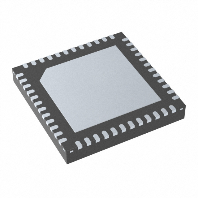


 工商网监
湘ICP备2023018690号
工商网监
湘ICP备2023018690号
