Product
Folder
Order
Now
Support &
Community
Tools &
Software
Technical
Documents
CD54HC4051, CD74HC4051
CD54HCT4051, CD74HCT4051, CD54HC4052, CD74HC4052, CD54HCT4052
CD74HCT4052, CD54HC4053, CD74HC4053, CD54HCT4053, CD74HCT4053
SCHS122M – NOVEMBER 1997 – REVISED MAY 2019
CDx4HC405x, CDx4HCT405x High-Speed CMOS Logic Analog
Multiplexers and Demultiplexers
1 Features
3 Description
•
•
The CDx4HC405x and CDx4HCT405x devices are
digitally controlled analog switches that use silicon
gate CMOS technology to achieve operating speeds
similar to LSTTL with the low-power consumption of
standard CMOS integrated circuits.
1
•
•
•
•
•
•
•
Wide Analog Input Voltage Range: ±5-V Maximum
Low ON-Resistance
– 70-Ω Typical (VCC – VEE = 4.5 V)
– 40-Ω Typical (VCC – VEE = 9 V)
Low Crosstalk Between Switches
Fast Switching and Propagation Speeds
Break-Before-Make Switching
Wide Operating Temperature Range:
–55°C to +125°C
CD54HC and CD74HC Types
– Operation Control Voltage: 2 V to 6 V
– Switch Voltage: 0 V to 10 V
CD54HCT and CD74HCT Types
– Operation Control Voltage: 4.5 V to 5.5 V
– Switch Voltage: 0 V to 10 V
– Direct LSTTL Input Logic Compatibility
VIL = 0.8-V Max, VIH = 2-V Min
– CMOS Input Compatibility
II ≤ 1 µA at VOL, VOH
On Products Compliant to MIL-PRF-38535,
All Parameters Are Tested Unless Otherwise
Noted. On All Other Products, Production
Processing Does Not Necessarily Include Testing
of All Parameters.
These analog multiplexers and demultiplexers control
analog voltages that may vary across the voltage
supply range (for example, VCC to VEE). They are
bidirectional switches that allow any analog input to
be used as an output and vice versa. The switches
have low ON resistance and low OFF leakages. In
addition, all these devices have an enable control
that, when high, disables all switches to their OFF
state.
Device Information(1)
PART NUMBER
Digital Radio
Signal Gating
Factory Automation
Televisions
Appliances
Programmable Logic Circuits
Sensors
BODY SIZE (NOM)
CDIP (16)
19.56 mm × 6.92 mm
CD74HCx405xE
PDIP (16)
19.30 mm × 6.35 mm
CD74HCx405xM
SOIC (16)
9.90 mm × 3.91 mm
CD74HCx405xNS
SOP (16)
10.30 mm × 5.30 mm
CD74HCx405xPW
TSSOP (16)
5.00 mm × 4.40 mm
(1) For all available packages, see the orderable addendum at
the end of the data sheet.
Functional Diagram of HC4051 and HCT4051
CHANNEL IN/OUT
VCC
A7
A6
A5
A4
A3
A2
A1
A0
16
4
2
5
1
12
15
14
13
2 Applications
•
•
•
•
•
•
•
PACKAGE
CD54HCx405xF
TG
TG
S0
11
TG
TG
S1
10
BINARY
TO
1 OF 8
DECODER
WITH
ENABLE
LOGIC
LEVEL
CONVERSION
S2
9
E
6
3
A
COMMON
OUT/IN
TG
TG
TG
TG
8
7
GND
VEE
1
An IMPORTANT NOTICE at the end of this data sheet addresses availability, warranty, changes, use in safety-critical applications,
intellectual property matters and other important disclaimers. PRODUCTION DATA.
�CD54HC4051, CD74HC4051
CD54HCT4051, CD74HCT4051, CD54HC4052, CD74HC4052, CD54HCT4052
CD74HCT4052, CD54HC4053, CD74HC4053, CD54HCT4053, CD74HCT4053
SCHS122M – NOVEMBER 1997 – REVISED MAY 2019
www.ti.com
Table of Contents
1
2
3
4
5
6
Features ..................................................................
Applications ...........................................................
Description .............................................................
Revision History.....................................................
Pin Configuration and Functions .........................
Specifications.........................................................
6.1
6.2
6.3
6.4
6.5
6.6
6.7
6.8
6.9
6.10
7
8
1
1
1
2
3
6
Absolute Maximum Ratings ...................................... 6
ESD Ratings ............................................................ 6
Recommended Operating Conditions ...................... 6
Thermal Information .................................................. 7
Electrical Characteristics: HC Devices...................... 7
Electrical Characteristics: HCT Devices ................. 10
Switching Characteristics, VCC = 5 V...................... 12
Switching Characteristics, CL = 50 pF .................... 13
Analog Channel Specifications ............................... 16
Typical Characteristics .......................................... 17
Parameter Measurement Information ................ 18
Detailed Description ............................................ 20
8.1 Overview ................................................................. 20
8.2 Functional Block Diagrams ..................................... 20
8.3 Feature Description................................................. 22
8.4 Device Functional Modes........................................ 22
9
Application and Implementation ........................ 23
9.1 Application Information............................................ 23
9.2 Typical Application ................................................. 23
10 Power Supply Recommendations ..................... 24
11 Layout................................................................... 25
11.1 Layout Guidelines ................................................. 25
11.2 Layout Example .................................................... 25
12 Device and Documentation Support ................. 26
12.1
12.2
12.3
12.4
12.5
12.6
12.7
Documentation Support ........................................
Related Links ........................................................
Receiving Notification of Documentation Updates
Community Resources..........................................
Trademarks ...........................................................
Electrostatic Discharge Caution ............................
Glossary ................................................................
26
26
26
26
26
26
27
13 Mechanical, Packaging, and Orderable
Information ........................................................... 27
4 Revision History
NOTE: Page numbers for previous revisions may differ from page numbers in the current version.
Changes from Revision L (February 2017) to Revision M
•
Page
Changed Feature From: 7-Ω Typical To: 70-Ω Typical ......................................................................................................... 1
Changes from Revision K (September 2015) to Revision L
Page
•
Changed Charged device model (CDM) value from: ±1000 V to: ±200 V ............................................................................. 6
•
Added Receiving Notification of Documentation Updates section ...................................................................................... 26
Changes from Revision J (February 2011) to Revision K
Page
•
Removed Ordering Information table. .................................................................................................................................... 1
•
Added Device Information table, Pin Functions table, ESD Ratings table, Thermal Information table, Detailed
Description section, Applications and Implementation section, Power Supply Recommendations section, Layout
section, Device and Documentation Support section, and Mechanical, Packaging, and Orderable Information section ...... 1
•
Added Military Disclaimer to Features list. ............................................................................................................................. 1
2
Submit Documentation Feedback
Copyright © 1997–2019, Texas Instruments Incorporated
Product Folder Links: CD54HC4051 CD74HC4051 CD54HCT4051 CD74HCT4051 CD54HC4052 CD74HC4052
CD54HCT4052 CD74HCT4052 CD54HC4053 CD74HC4053 CD54HCT4053 CD74HCT4053
�CD54HC4051, CD74HC4051
CD54HCT4051, CD74HCT4051, CD54HC4052, CD74HC4052, CD54HCT4052
CD74HCT4052, CD54HC4053, CD74HC4053, CD54HCT4053, CD74HCT4053
www.ti.com
SCHS122M – NOVEMBER 1997 – REVISED MAY 2019
5 Pin Configuration and Functions
CD54HC4051, CD54HCT4051, CD74HC4051, CD74HCT4051 J, N, D, NS, PW Packages
16-Pin CDIP, PDIP, SOIC, SO, TSSOP
Top View
CHANNEL
IN/OUT
COM OUT/IN
CHANNEL
IN/OUT
A4 1
16 VCC
A6 2
15 A2
A 3
14 A1
A7 4
13 A0
A5 5
12 A3
E 6
11 S0
7
10 S1
GND 8
9 S2
VEE
CHANNEL
IN/OUT
ADDRESS
SELECT
Pin Functions for CDx4HCx4051B
PIN
NO.
NAME
I/O
DESCRIPTION
1
CH A4 IN/OUT
I/O
Channel 4 in/out
2
CH A6 IN/OUT
I/O
Channel 6 in/out
3
COM OUT/IN
I/O
Common out/in
4
CH A7 IN/OUT
I/O
Channel 7 in/out
5
CH A5 IN/OUT
I/O
Channel 5 in/out
6
E
I
7
VEE
—
Negative power input
8
GND
—
Ground
9
S2
I
Channel select 2. See Table 1.
10
S1
I
Channel select 1. See Table 1.
11
S0
I
Channel select 0. See Table 1.
12
CH A3 IN/OUT
I/O
Channel 3 in/out
13
CH A0 IN/OUT
I/O
Channel 0 in/out
14
CH A1 IN/OUT
I/O
Channel 1 in/out
15
CH A2 IN/OUT
I/O
Channel 2 in/out
16
VCC
—
Positive power input
Copyright © 1997–2019, Texas Instruments Incorporated
Enable Channels (Active Low). See Table 1.
Submit Documentation Feedback
Product Folder Links: CD54HC4051 CD74HC4051 CD54HCT4051 CD74HCT4051 CD54HC4052 CD74HC4052
CD54HCT4052 CD74HCT4052 CD54HC4053 CD74HC4053 CD54HCT4053 CD74HCT4053
3
�CD54HC4051, CD74HC4051
CD54HCT4051, CD74HCT4051, CD54HC4052, CD74HC4052, CD54HCT4052
CD74HCT4052, CD54HC4053, CD74HC4053, CD54HCT4053, CD74HCT4053
SCHS122M – NOVEMBER 1997 – REVISED MAY 2019
www.ti.com
CD54HC4052, CD74HC4052, CD74HCT4052 J, N, D, NS, PW Packages
16-Pin CDIP, PDIP, SOIC, SO, TSSOP
Top View
CHANNEL
IN/OUT
B0 1
16 VCC
B2 2
15 A2
3
14 A1
CHANNEL
IN/OUT
B3 4
13 AN
COM OUT/IN
B1 5
12 A0
E 6
11 A3
COM OUT/IN BN
CHANNEL
IN/OUT
VEE
7
10 S0
GND
8
9 S1
CHANNEL
IN/OUT
Pin Functions for CDx4HCx4052B
PIN
NO.
1
NAME
I/O
DESCRIPTION
CH B0 IN/OUT
I/O
Channel B0 in/out
2
CH B2 IN/OUT
I/O
Channel B2 in/out
3
COM B OUT/IN
I/O
B common out/in
4
CH B3 IN/OUT
I/O
Channel B3 in/out
5
CH B1 IN/OUT
I/O
Channel B1 in/out
6
E
I
7
VEE
—
Negative power input
8
GND
—
Ground
9
S1
I
Channel select 1. See Table 2.
10
S0
I
Channel select 0. See Table 2.
11
CH A3 IN/OUT
I/O
Channel A3 in/out
12
CH A0 IN/OUT
I/O
Channel A0 in/out
13
COM A IN/OUT
I/O
A common out/in
14
CH A1 IN/OUT
I/O
Channel A1 in/out
15
CH A2 IN/OUT
I/O
Channel A2 in/out
16
VCC
—
Positive power input
4
Submit Documentation Feedback
Enable channels (Active Low). See Table 2.
Copyright © 1997–2019, Texas Instruments Incorporated
Product Folder Links: CD54HC4051 CD74HC4051 CD54HCT4051 CD74HCT4051 CD54HC4052 CD74HC4052
CD54HCT4052 CD74HCT4052 CD54HC4053 CD74HC4053 CD54HCT4053 CD74HCT4053
�CD54HC4051, CD74HC4051
CD54HCT4051, CD74HCT4051, CD54HC4052, CD74HC4052, CD54HCT4052
CD74HCT4052, CD54HC4053, CD74HC4053, CD54HCT4053, CD74HCT4053
www.ti.com
SCHS122M – NOVEMBER 1997 – REVISED MAY 2019
CD54HC4053 CD74HC4053 CD74HCT4053 J, N, D, NS, PW Packages
16-Pin CDIP, PDIP, SOIC, SOP, TSSOP
TOP VIEW
CHANNEL
IN/OUT
B1 1
16 VCC
B0 2
15 BN
COM OUT/IN
C1 3
14 AN
COM OUT/IN
COM OUT/IN CN
4
13 A1
IN/OUT C0 5
12 A0
E 6
11 S0
VEE
7
10 S1
GND
8
9 S2
CHANNEL
IN/OUT
Pin Functions CDx4HCx4053B
PIN
NO.
1
NAME
I/O
DESCRIPTION
B1 IN/OUT
I/O
B channel Y in/out
2
B0 IN/OUT
I/O
B channel X in/out
3
C1 IN/OUT
I/O
C channel Y in/out
4
COM C OUT/IN
I/O
C common out/in
5
C0 IN/OUT
I/O
C channel X in/out
6
E
I
7
VEE
—
Negative power input
8
GND
—
Ground
9
S2
I
Channel select 2. See Table 3.
10
S1
I
Channel select 1. See Table 3.
11
S0
I
Channel select 0. See Table 3.
12
A0 IN/OUT
I/O
A channel X in/out
13
A1 IN/OUT
I/O
A channel Y in/out
14
COM A OUT/IN
I/O
A common out/in
15
COM B OUT/IN
I/O
B common out/in
16
VCC
—
Positive power input
Copyright © 1997–2019, Texas Instruments Incorporated
Enable channels (Active Low). See Table 3.
Submit Documentation Feedback
Product Folder Links: CD54HC4051 CD74HC4051 CD54HCT4051 CD74HCT4051 CD54HC4052 CD74HC4052
CD54HCT4052 CD74HCT4052 CD54HC4053 CD74HC4053 CD54HCT4053 CD74HCT4053
5
�CD54HC4051, CD74HC4051
CD54HCT4051, CD74HCT4051, CD54HC4052, CD74HC4052, CD54HCT4052
CD74HCT4052, CD54HC4053, CD74HC4053, CD54HCT4053, CD74HCT4053
SCHS122M – NOVEMBER 1997 – REVISED MAY 2019
www.ti.com
6 Specifications
6.1 Absolute Maximum Ratings
over operating free-air temperature range (unless otherwise noted) (1)
MIN
MAX
UNIT
VCC – VEE DC supply voltage
–0.5
10.5
V
VCC
DC supply voltage
–0.5
7
V
VEE
DC supply voltage
0.5
–7
V
IIK
DC input diode current
VI < – 0.5 V or VI > VCC + 0.5 V
±20
mA
IOK
DC switch diode current
VI < VEE – 0.5 V or VI > VCC + 0.5 V
±20
mA
DC switch current (2)
VI > VEE – 0.5 V or VI < VCC + 0.5 V
±25
mA
ICC
DC VCC or ground current
±50
mA
IEE
DC VEE current
–20
mA
TJMAX
Maximum junction temperature
150
°C
TLMAX
Maximum lead temperature
300
°C
TJ
Junction temperature
150
°C
Tstg
Storage temperature
150
°C
(1)
(2)
Soldering 10 s
–65
Stresses beyond those listed under Absolute Maximum Ratings may cause permanent damage to the device. These are stress ratings
only, and functional operation of the device at these or any other conditions beyond those indicated under Recommended Operating
Conditions is not implied. Exposure to absolute-maximum-rated conditions for extended periods may affect device reliability.
All voltages referenced to GND unless otherwise specified.
6.2 ESD Ratings
VALUE
V(ESD)
(1)
(2)
Electrostatic discharge
Human body model (HBM), per ANSI/ESDA/JEDEC JS-001 (1)
±500
Charged device model (CDM), per JEDEC specification JESD22-C101 or
ANSI/ESDA/JEDEC JS-002 (2)
±200
UNIT
V
JEDEC document JEP155 states that 500-V HBM allows safe manufacturing with a standard ESD control process.
JEDEC document JEP157 states that 250-V CDM allows safe manufacturing with a standard ESD control process.
6.3 Recommended Operating Conditions
over operating free-air temperature range (unless otherwise noted) (1)
MIN
CD54 and 74HC types
VCC
Supply voltage range
(TA = full package temperature
range) (2)
VCC –
VEE
Supply voltage range
(TA = full package temperature range)
VEE
Supply voltage range
(TA = full package temperature
range) (3)
VI
DC input control voltage
VIS
Analog switch I/O voltage
TA
Operating temperature
tr, tf
(1)
(2)
(3)
6
Input rise and fall times
NOM
MAX UNIT
2
6
4.5
5.5
CD54 and 74HC types, CD54 and 74HCT
types (see Figure 1)
2
10
V
CD54 and 74HC types, CD54 and 74HCT
types (see Figure 2)
0
–6
V
GND
VCC
V
VEE
VCC
V
°C
CD54 and 74HCT types
–55
125
2V
0
1000
4.5 V
0
500
6V
0
400
V
ns
For maximum reliability, nominal operating conditions must be selected so that operation is always within the ranges specified in the
Recommended Operating Conditions table.
All voltages referenced to GND unless otherwise specified.
In certain applications, the external load resistor current may include both VCC and signal line components. To avoid drawing VCC
current when switch current flows into the transmission gate inputs, the voltage drop across the bidirectional switch must not exceed
0.6 V (calculated from rON values shown in Electrical Characteristics: HC Devices and Electrical Characteristics: HCT Devices tables).
No VCC current will flow through RL if the switch current flows into terminal 3 on the HC and HCT4051; terminals 3 and 13 on the HC
and HCT4052; terminals 4, 14, and 15 on the HC and HCT4053.
Submit Documentation Feedback
Copyright © 1997–2019, Texas Instruments Incorporated
Product Folder Links: CD54HC4051 CD74HC4051 CD54HCT4051 CD74HCT4051 CD54HC4052 CD74HC4052
CD54HCT4052 CD74HCT4052 CD54HC4053 CD74HC4053 CD54HCT4053 CD74HCT4053
�CD54HC4051, CD74HC4051
CD54HCT4051, CD74HCT4051, CD54HC4052, CD74HC4052, CD54HCT4052
CD74HCT4052, CD54HC4053, CD74HC4053, CD54HCT4053, CD74HCT4053
www.ti.com
SCHS122M – NOVEMBER 1997 – REVISED MAY 2019
6.4 Thermal Information
CD74HC4051
THERMAL METRIC (1)
N (PDIP)
NS (SO)
PW (TSSOP)
16 PINS
16 PINS
16 PINS
UNIT
RθJA
Junction-to-ambient thermal resistance
49.0
83.0
107.7
°C/W
RθJC(top)
Junction-to-case (top) thermal resistance
36.3
41.2
42.4
°C/W
RθJB
Junction-to-board thermal resistance
29.0
43.3
52.8
°C/W
ψJT
Junction-to-top characterization parameter
21.2
9.2
4.2
°C/W
ψJB
Junction-to-board characterization parameter
28.9
43.0
52.2
°C/W
(1)
For more information about traditional and new thermal metrics, see the Semiconductor and IC Package Thermal Metrics application
report.
6.5 Electrical Characteristics: HC Devices
TEST CONDITIONS
PARAMETERS
VIH
VIS
(V)
High-level input voltage
VI
(V)
VEE
(V)
TA
25°C
1.5
2
–40°C to
+85°C
1.5
–55°C to
+125°C
1.5
4.5
6
2
VIL
Low-level input voltage
4.5
6
Copyright © 1997–2019, Texas Instruments Incorporated
MIN
VCC
(V)
25°C
3.15
–40°C to
+85°C
3.15
–55°C to
+125°C
3.15
25°C
4.2
–40°C to
+85°C
4.2
–55°C to
+125°C
4.2
TYP
MAX
UNIT
V
25°C
0.5
–40°C to
+85°C
0.5
–55°C to
+125°C
0.5
25°C
1.35
–40°C to
+85°C
1.35
–55°C to
+125°C
1.35
25°C
1.8
–40°C to
+85°C
1.8
–55°C to
+125°C
1.8
Submit Documentation Feedback
Product Folder Links: CD54HC4051 CD74HC4051 CD54HCT4051 CD74HCT4051 CD54HC4052 CD74HC4052
CD54HCT4052 CD74HCT4052 CD54HC4053 CD74HC4053 CD54HCT4053 CD74HCT4053
V
7
�CD54HC4051, CD74HC4051
CD54HCT4051, CD74HCT4051, CD54HC4052, CD74HC4052, CD54HCT4052
CD74HCT4052, CD54HC4053, CD74HC4053, CD54HCT4053, CD74HCT4053
SCHS122M – NOVEMBER 1997 – REVISED MAY 2019
www.ti.com
Electrical Characteristics: HC Devices (continued)
TEST CONDITIONS
PARAMETERS
VIS
(V)
VI
(V)
VEE
(V)
0
rON
ON
resistance
–55°C to
+125°C
240
6
4.5
4.5
–55°C to
+125°C
210
0
6
ΔrON
8
Maximum ON resistance
between any two channels
Submit Documentation Feedback
4.5
120
–40°C to
+85°C
150
–55°C to
+125°C
180
90
180
–40°C to
+85°C
225
–55°C to
+125°C
270
80
200
–55°C to
+125°C
240
45
130
–40°C to
+85°C
162
–55°C to
+125°C
195
0
4.5
25°C
10
0
6
25°C
8.5
–4.5
4.5
25°C
5
Ω
160
–40°C to
+85°C
25°C
–4.5
40
UNIT
140
175
25°C
VCC to VEE
60
–40°C to
+85°C
25°C
0
160
200
VIL
or
VIH
IO = 1 mA
See Figure 21
70
4.5
25°C
–4.5
MAX
–40°C to
+85°C
25°C
VCC or VEE
TYP
TA
25°C
0
MIN
VCC
(V)
Ω
Copyright © 1997–2019, Texas Instruments Incorporated
Product Folder Links: CD54HC4051 CD74HC4051 CD54HCT4051 CD74HCT4051 CD54HC4052 CD74HC4052
CD54HCT4052 CD74HCT4052 CD54HC4053 CD74HC4053 CD54HCT4053 CD74HCT4053
�CD54HC4051, CD74HC4051
CD54HCT4051, CD74HCT4051, CD54HC4052, CD74HC4052, CD54HCT4052
CD74HCT4052, CD54HC4053, CD74HC4053, CD54HCT4053, CD74HCT4053
www.ti.com
SCHS122M – NOVEMBER 1997 – REVISED MAY 2019
Electrical Characteristics: HC Devices (continued)
TEST CONDITIONS
PARAMETERS
VIS
(V)
VI
(V)
VEE
(V)
MIN
0
6
–40°C to
+85°C
±1
–55°C to
+125°C
±1
25°C
4053
–5
5
4 channels
IIZ
Switch
ON/OFF
leakage
current
4052
0
6
VIL
or
VIH
–5
5
–55°C to
+125°C
±1
0
6
±1
–55°C to
+125°C
±1
–5
5
±2
–55°C to
+125°C
±2
IIL
Control input leakage current
When VIS = VEE,
VOS = VCC
ICC
Quiescent
device
current
0
0
6
6
VCC
or
GND
IO = 0
When VIS = VCC,
VOS = VEE
Copyright © 1997–2019, Texas Instruments Incorporated
–5
5
µA
±0.2
–40°C to
+85°C
±2
–55°C to
+125°C
±2
±0.4
–40°C to
+85°C
±4
–55°C to
+125°C
±4
25°C
VCC
or
GND
±0.2
–40°C to
+85°C
25°C
4051
±0.1
–40°C to
+85°C
25°C
8 channels
±0.1
±1
25°C
UNIT
±0.1
–40°C to
+85°C
25°C
For switch OFF:
When VIS = VCC,
VOS = VEE;
When VIS = VEE,
VOS = VCC,
For switch ON:
All applicable
combinations of
VIS and VOS
voltage levels
MAX
TA
25°C
1 and 2
channels
TYP
VCC
(V)
±0.1
–40°C to
+85°C
±1
–55°C to
+125°C
±1
25°C
8
–40°C to
+85°C
80
–55°C to
+125°C
160
25°C
16
–40°C to
+85°C
160
–55°C to
+125°C
320
Submit Documentation Feedback
Product Folder Links: CD54HC4051 CD74HC4051 CD54HCT4051 CD74HCT4051 CD54HC4052 CD74HC4052
CD54HCT4052 CD74HCT4052 CD54HC4053 CD74HC4053 CD54HCT4053 CD74HCT4053
µA
µA
9
�CD54HC4051, CD74HC4051
CD54HCT4051, CD74HCT4051, CD54HC4052, CD74HC4052, CD54HCT4052
CD74HCT4052, CD54HC4053, CD74HC4053, CD54HCT4053, CD74HCT4053
SCHS122M – NOVEMBER 1997 – REVISED MAY 2019
www.ti.com
6.6 Electrical Characteristics: HCT Devices
TEST CONDITIONS
PARAMETER
VIH
VIL
VIS
(V)
VI
(V)
VEE
(V)
VCC
(V)
4.5
to
5.5
High-level input voltage
4.5
to
5.5
Low-level input voltage
TA
25°C
2
–40°C to
+85°C
2
–55°C to
+125°C
2
4.5
VCC or VEE
rON
ON resistance
4.5
VIL
or
VIH
IO = 1 mA
See Figure 6
4.5
VCC to VEE
0.8
–55°C to
+125°C
0.8
–4.5
ΔrON
10
Maximum ON resistance
between any two channels
Submit Documentation Feedback
4.5
70
200
–55°C to
+125°C
240
40
120
–40°C to
+85°C
150
–55°C to
+125°C
180
90
180
–40°C to
+85°C
225
–55°C to
+125°C
270
45
162
–55°C to
+125°C
195
0
4.5
25°C
10
4.5
25°C
5
Ω
130
–40°C to
+85°C
–4.5
V
160
–40°C to
+85°C
25°C
UNIT
V
0.8
25°C
0
MAX
25°C
25°C
–4.5
TYP
–40°C to
+85°C
25°C
0
MIN
Ω
Copyright © 1997–2019, Texas Instruments Incorporated
Product Folder Links: CD54HC4051 CD74HC4051 CD54HCT4051 CD74HCT4051 CD54HC4052 CD74HC4052
CD54HCT4052 CD74HCT4052 CD54HC4053 CD74HC4053 CD54HCT4053 CD74HCT4053
�CD54HC4051, CD74HC4051
CD54HCT4051, CD74HCT4051, CD54HC4052, CD74HC4052, CD54HCT4052
CD74HCT4052, CD54HC4053, CD74HC4053, CD54HCT4053, CD74HCT4053
www.ti.com
SCHS122M – NOVEMBER 1997 – REVISED MAY 2019
Electrical Characteristics: HCT Devices (continued)
TEST CONDITIONS
PARAMETER
VIS
(V)
VI
(V)
VEE
(V)
MIN
TYP
TA
6
–40°C to
+85°C
±1
–55°C to
+125°C
±1
25°C
1 and 2
channels
0
–5
5
±0.1
–40°C to
+85°C
±1
–55°C to
+125°C
±1
25°C
4 channels
IIZ
Switch
ON/OFF
leakage
current
4052
For switch OFF:
When VIS = VCC,
VOS = VEE;
When VIS = VEE,
VOS = VCC
For switch ON:
All applicable
combinations of
VIS and VOS
voltage levels
0
6
VIL
or
VIH
±0.1
–40°C to
+85°C
±1
–55°C to
+125°C
±1
25°C
–5
5
±0.2
–40°C to
+85°C
±2
–55°C to
+125°C
±2
25°C
8 channels
0
6
–5
5
±2
–55°C to
+125°C
±2
±0.4
–40°C to
+85°C
±4
–55°C to
+125°C
±4
25°C
IIL
See (1)
Control input leakage current
When VIS = VEE,
VOS = VCC
ICC
Quiescent
device
current
5.5
0
5.5
VCC
or
GND
IO = 0
When VIS = VCC,
VOS = VEE
–4.5
5.5
±0.1
–40°C to
+85°C
±1
–55°C to
+125°C
±1
25°C
8
–40°C to
+85°C
80
–55°C to
+125°C
160
25°C
16
–40°C to
+85°C
160
–55°C to
+125°C
320
25°C
ΔICC
(1)
(2)
Additional quiescent
device current per input pin:
1 unit load (2)
ΔICC (2)
VCC – 2.1
4.5 to 5.5
µA
±0.2
–40°C to
+85°C
25°C
4051
UNIT
±0.1
25°C
4053
MAX
VCC
(V)
100
µA
µA
µA
360
–40°C to
+85°C
450
–55°C to
+125°C
490
µA
Any voltage between VCC and GND.
For dual-supply systems, theoretical worst-case (VI = 2.4 V, VCC = 5.5 V) specification is 1.8 mA.
Copyright © 1997–2019, Texas Instruments Incorporated
Submit Documentation Feedback
Product Folder Links: CD54HC4051 CD74HC4051 CD54HCT4051 CD74HCT4051 CD54HC4052 CD74HC4052
CD54HCT4052 CD74HCT4052 CD54HC4053 CD74HC4053 CD54HCT4053 CD74HCT4053
11
�CD54HC4051, CD74HC4051
CD54HCT4051, CD74HCT4051, CD54HC4052, CD74HC4052, CD54HCT4052
CD74HCT4052, CD54HC4053, CD74HC4053, CD54HCT4053, CD74HCT4053
SCHS122M – NOVEMBER 1997 – REVISED MAY 2019
www.ti.com
6.7 Switching Characteristics, VCC = 5 V
VCC = 5 V, TA = 25°C, input tr, tf = 6 ns
PARAMETER
tPHL, tPLH
tPHZ, tPLZ
Switch IN to OUT
Propagation delay
tPZH, tPZL
CPD
TEST CONDITIONS
Switch turn-off (S or E)
Switch turn-on (S or E)
Power dissipation
capacitance (1)
CL
(pF)
MIN
CDx4HC4051
4
CDx4HCT4051
4
CDx4HC4052
CDx4HCT4052
4
CDx4HC4053
4
CDx4HCT4053
4
CDx4HC4051
19
CDx4HCT4051
19
CDx4HC4052
CDx4HCT4052
21
15
21
CDx4HC4053
18
CDx4HCT4053
18
CDx4HC4051
19
CDx4HCT4051
23
CDx4HC4052
CDx4HCT4052
27
15
29
CDx4HC4053
18
CDx4HCT4053
20
CDx4HC4051
50
CDx4HCT4051
52
CDx4HC4052
74
CDx4HCT4052
76
CDx4HC4053
38
12
CPD is used to determine the dynamic power consumption, per
fI = input frequency, CL = output load capacitance, CS = switch
Submit Documentation Feedback
MAX
4
15
CDx4HCT4053
(1)
TYP
UNIT
ns
ns
ns
pF
42
package. PD = CPD VCC2 fI
capacitance, VCC = supply
+ ∑ (CL +
voltage
CS) VCC2 fO
, fO = output frequency,
Copyright © 1997–2019, Texas Instruments Incorporated
Product Folder Links: CD54HC4051 CD74HC4051 CD54HCT4051 CD74HCT4051 CD54HC4052 CD74HC4052
CD54HCT4052 CD74HCT4052 CD54HC4053 CD74HC4053 CD54HCT4053 CD74HCT4053
�CD54HC4051, CD74HC4051
CD54HCT4051, CD74HCT4051, CD54HC4052, CD74HC4052, CD54HCT4052
CD74HCT4052, CD54HC4053, CD74HC4053, CD54HCT4053, CD74HCT4053
www.ti.com
SCHS122M – NOVEMBER 1997 – REVISED MAY 2019
6.8 Switching Characteristics, CL = 50 pF
CL = 50 pF, input tr, tf = 6 ns
PARAMETER
VEE
(V)
VCC
(V)
0
2
0
tPLH,
tPHL
Propagation delay,
switch in to out
0
–4.5
0
tPHZ,
tPLZ
Maximum
switch turn
OFF delay
4051
from S or E
to switch output
0
0
–4.5
0
0
tPHZ,
tPLZ
4.5
Maximum
switch turn
OFF delay
4052
from S or E
to switch output
0
6
4.5
2
4.5
6
4.5
2
4.5
6
TEST CONDITIONS
4.5
HC
60
TA = –40°C to +85°C
HC
75
TA = –55°C to +125°C
HC
90
TA = 25°C
HC, HCT
12
TA = –40°C to +85°C
HC, HCT
15
TA = –55°C to +125°C
HC, HCT
18
TA = 25°C
HC
10
TA = –40°C to +85°C
HC
13
TA = –55°C to +125°C
HC
15
TA = 25°C
HC, HCT
8
TA = –40°C to +85°C
HC, HCT
10
TA = –55°C to +125°C
HC, HCT
TA = 25°C
HC
225
TA = –40°C to +85°C
HC
280
TA = –55°C to +125°C
HC
340
TA = 25°C
HC, HCT
45
TA = –40°C to +85°C
HC, HCT
56
TA = –55°C to +125°C
HC, HCT
68
TA = 25°C
HC
38
TA = –40°C to +85°C
HC
48
TA = –55°C to +125°C
HC
57
TA = 25°C
HC, HCT
32
TA = –40°C to +85°C
HC, HCT
40
TA = –55°C to +125°C
HC, HCT
TA = 25°C
HC
250
TA = –40°C to +85°C
HC
315
TA = –55°C to +125°C
HC
375
TA = 25°C
HC, HCT
50
TA = –40°C to +85°C
HC, HCT
63
TA = –55°C to +125°C
HC, HCT
75
TA = 25°C
HC
43
TA = –40°C to +85°C
HC
54
TA = –55°C to +125°C
HC
65
HC
38
HCT
38
HC
48
HCT
48
HC
57
HCT
57
TA = –40°C to +85°C
TA = –55°C to +125°C
Copyright © 1997–2019, Texas Instruments Incorporated
MAX
TA = 25°C
TA = 25°C
–4.5
MIN
UNIT
ns
12
ns
48
Submit Documentation Feedback
Product Folder Links: CD54HC4051 CD74HC4051 CD54HCT4051 CD74HCT4051 CD54HC4052 CD74HC4052
CD54HCT4052 CD74HCT4052 CD54HC4053 CD74HC4053 CD54HCT4053 CD74HCT4053
ns
13
�CD54HC4051, CD74HC4051
CD54HCT4051, CD74HCT4051, CD54HC4052, CD74HC4052, CD54HCT4052
CD74HCT4052, CD54HC4053, CD74HC4053, CD54HCT4053, CD74HCT4053
SCHS122M – NOVEMBER 1997 – REVISED MAY 2019
www.ti.com
Switching Characteristics, CL = 50 pF (continued)
CL = 50 pF, input tr, tf = 6 ns
PARAMETER
VEE
(V)
VCC
(V)
0
2
TEST CONDITIONS
tPHZ,
tPLZ
Maximum
switch turn
OFF delay
4053
from S or E
to switch output
4.5
HC
210
TA = –40°C to +85°C
HC
265
TA = –55°C to +125°C
HC
315
HC
42
HCT
44
HC
53
HCT
53
HC
63
TA = –40°C to +85°C
TA = –55°C to +125°C
0
6
HCT
66
TA = 25°C
HC
36
TA = –40°C to +85°C
HC
45
TA = –55°C to +125°C
HC
54
HC
29
HCT
31
HC
36
HCT
39
HC
44
TA = 25°C
–4.5
4.5
TA = –40°C to +85°C
TA = –55°C to +125°C
0
2
tPZL,
tPZH
Maximum
switch turn
ON delay
4051
from S or E
to switch output
4.5
225
TA = –40°C to +85°C
HC
280
TA = –55°C to +125°C
HC
340
HC
45
HCT
55
HC
56
HCT
69
HC
68
HCT
83
TA = 25°C
HC
38
TA = –40°C to +85°C
HC
48
TA = –55°C to +125°C
HC
57
HC
32
HCT
39
HC
40
HCT
49
HC
48
HCT
59
TA = –40°C to +85°C
6
TA = 25°C
–4.5
4.5
TA = –40°C to +85°C
TA = –55°C to +125°C
14
Submit Documentation Feedback
UNIT
ns
47
HC
TA = –55°C to +125°C
0
HCT
TA = 25°C
TA = 25°C
0
MAX
TA = 25°C
TA = 25°C
0
MIN
ns
Copyright © 1997–2019, Texas Instruments Incorporated
Product Folder Links: CD54HC4051 CD74HC4051 CD54HCT4051 CD74HCT4051 CD54HC4052 CD74HC4052
CD54HCT4052 CD74HCT4052 CD54HC4053 CD74HC4053 CD54HCT4053 CD74HCT4053
�CD54HC4051, CD74HC4051
CD54HCT4051, CD74HCT4051, CD54HC4052, CD74HC4052, CD54HCT4052
CD74HCT4052, CD54HC4053, CD74HC4053, CD54HCT4053, CD74HCT4053
www.ti.com
SCHS122M – NOVEMBER 1997 – REVISED MAY 2019
Switching Characteristics, CL = 50 pF (continued)
CL = 50 pF, input tr, tf = 6 ns
PARAMETER
VEE
(V)
VCC
(V)
0
2
TEST CONDITIONS
tPZL,
tPZH
Maximum
switch turn
ON delay
4052
from S or E
to switch output
4.5
HC
325
TA = –40°C to +85°C
HC
405
TA = –55°C to +125°C
HC
490
HC
65
HCT
70
HC
81
HCT
68
HC
98
TA = –40°C to +85°C
TA = –55°C to +125°C
0
6
4.5
55
TA = –40°C to +85°C
HC
69
TA = –55°C to +125°C
HC
83
HC
46
HCT
48
HC
58
HCT
60
HC
69
TA = –40°C to +85°C
2
tPZL,
tPZH
Maximum
switch turn
ON delay
4053
from S or E
to switch output
4.5
HC
220
TA = –40°C to +85°C
HC
275
TA = –55°C to +125°C
HC
330
HC
44
HCT
48
HC
55
HCT
60
HC
66
HCT
72
TA = 25°C
HC
37
TA = –40°C to +85°C
HC
47
TA = –55°C to +125°C
HC
56
HC
31
HCT
34
HC
39
HCT
43
HC
47
HCT
51
TA = 25°C
HC, HCT
10
TA = –40°C to +85°C
HC, HCT
10
TA = –55°C to +125°C
HC, HCT
10
TA = –40°C to +85°C
TA = –55°C to +125°C
0
6
TA = 25°C
–4.5
4.5
TA = –40°C to +85°C
TA = –55°C to +125°C
CI
Input (control)
capacitance
Copyright © 1997–2019, Texas Instruments Incorporated
ns
72
TA = 25°C
TA = 25°C
0
HCT
UNIT
105
HC
TA = –55°C to +125°C
0
HCT
TA = 25°C
TA = 25°C
–4.5
MAX
TA = 25°C
TA = 25°C
0
MIN
Submit Documentation Feedback
Product Folder Links: CD54HC4051 CD74HC4051 CD54HCT4051 CD74HCT4051 CD54HC4052 CD74HC4052
CD54HCT4052 CD74HCT4052 CD54HC4053 CD74HC4053 CD54HCT4053 CD74HCT4053
ns
pF
15
�CD54HC4051, CD74HC4051
CD54HCT4051, CD74HCT4051, CD54HC4052, CD74HC4052, CD54HCT4052
CD74HCT4052, CD54HC4053, CD74HC4053, CD54HCT4053, CD74HCT4053
SCHS122M – NOVEMBER 1997 – REVISED MAY 2019
www.ti.com
6.9 Analog Channel Specifications
Typical values at TA = 25°C
PARAMETER
CI
TEST CONDITIONS
HC, HCT TYPES
Switch input capacitance
CCOM
fMAX
Common output capacitance
Minimum switch frequency
response at –3 dB
(see Figure 3, Figure 5, and
Figure 7)
VCC
(V)
TYP
All
5
4051
25
4052
12
4053
8
4051
145
4052
See Figure 10 (1) (2)
VEE
(V)
–2.25
2.25
200
4051
180
–4.5
4.5
–2.25%
2.25%
0.035%
All
–4.5%
4.5%
0.018%
4051
–2.25
2.25
–73
4052
Switch OFF signal feedthrough
(see Figure 4, Figure 6, and
Figure 8)
(1)
(2)
(3)
–65
4053
See Figure 14 (2) (3)
MHz
200
All
See Figure 12
pF
185
4053
Sine-wave distortion
pF
165
4053
4052
UNIT
–64
4051
–4.5
4.5
–75
4052
–67
4053
–66
dB
Adjust input voltage to obtain 0 dBm at VOS for fIN = 1 MHz.
VIS is centered at (VCC – VEE) / 2.
Adjust input for 0 dBm.
VCC − GND (V)
8
6
HCT
HC
4
2
0
0
2
4
6
8
10
12
VCC − VEE (V)
Figure 1. Recommended Operating Area as a Function of (VCC – VEE)
VCC − GND (V)
8
6
HCT
HC
4
2
0
0
−2
−4
−6
−8
VEE − GND (V)
Figure 2. Recommended Operating Area as a Function of (VEE – GND)
16
Submit Documentation Feedback
Copyright © 1997–2019, Texas Instruments Incorporated
Product Folder Links: CD54HC4051 CD74HC4051 CD54HCT4051 CD74HCT4051 CD54HC4052 CD74HC4052
CD54HCT4052 CD74HCT4052 CD54HC4053 CD74HC4053 CD54HCT4053 CD74HCT4053
�CD54HC4051, CD74HC4051
CD54HCT4051, CD74HCT4051, CD54HC4052, CD74HC4052, CD54HCT4052
CD74HCT4052, CD54HC4053, CD74HC4053, CD54HCT4053, CD74HCT4053
www.ti.com
SCHS122M – NOVEMBER 1997 – REVISED MAY 2019
6.10 Typical Characteristics
0
0
VCC = 4.5 V
GND = −4.5 V
VEE = −4.5 V
RL = 50 Ω
PIN 12 TO 3
−2
−4
−20
−40
dB
dB
VCC = 2.25 V
GND = −2.25 V
VEE = −2.25 V
RL = 50 Ω
PIN 12 TO 3
−6
−60
100K
1M
FREQUENCY (Hz)
10M
100M
−100
10K
100K
1M
10M
100M
FREQUENCY (Hz)
Figure 3. Channel ON Bandwidth
(HC and HCT4051)
Figure 4. Channel OFF Feedthrough
(HC and HCT4051)
0
0
VCC = 4.5 V
GND = −4.5 V
VEE = −4.5 V
RL = 50 Ω
PIN 4 TO 3
−4
−40
dB
VCC = 2.25 V
GND = −2.25 V
VEE = −2.25 V
RL = 50 Ω
PIN 4 TO 3
−6
VCC = 2.25 V
GND = −2.25 V
VEE = −2.25 V
RL = 50 Ω
PIN 4 TO 3
−20
dB
−2
−60
VCC = 4.5 V
GND = −4.5 V
VEE = −4.5V
RL = 50 Ω
PIN 4 TO 3
−80
−8
−10
10K
VCC = 4.5 V
GND = −4.5 V
VEE = −4.5 V
RL = 50 Ω
PIN 12 TO 3
−80
−8
−10
10K
VCC = 2.25 V
GND = −2.25 V
VEE = −2.25 V
RL = 50 Ω
PIN 12 TO 3
100K
1M
FREQUENCY (Hz)
10M
100M
−100
10K
100K
1M
FREQUENCY (Hz)
10M
100M
Figure 6. Channel OFF Feedthrough
(HC and HCT4052)
Figure 5. Channel ON Bandwidth
(HC and HCT4052)
0
0
VCC = 2.25 V
GND = −2.25 V
VEE = −2.25 V
RL = 50 Ω
PIN 5 TO 4
−20
VCC = 4.5 V
GND = −4.5 V
VEE = −4.5 V
RL = 50 Ω
PIN 5 TO 4
−2
−40
dB
dB
−1
VCC = 4.5 V
GND = −4.5 V
VEE = −4.5 V
RL = 50 Ω
PIN 5 TO 4
−60
VCC = 2.25 V
GND = −2.25 V
VEE = −2.25 V
RL = 50 Ω
PIN 5 TO 4
−3
−4
10K
100K
1M
FREQUENCY (Hz)
10M
Figure 7. Channel ON Bandwidth
(HC and HCT4053)
Copyright © 1997–2019, Texas Instruments Incorporated
−80
100M
−100
10K
100K
1M
FREQUENCY (Hz)
10M
100M
Figure 8. Channel OFF Feedthrough
(HC and HCT4053)
Submit Documentation Feedback
Product Folder Links: CD54HC4051 CD74HC4051 CD54HCT4051 CD74HCT4051 CD54HC4052 CD74HC4052
CD54HCT4052 CD74HCT4052 CD54HC4053 CD74HC4053 CD54HCT4053 CD74HCT4053
17
�CD54HC4051, CD74HC4051
CD54HCT4051, CD74HCT4051, CD54HC4052, CD74HC4052, CD54HCT4052
CD74HCT4052, CD54HC4053, CD74HC4053, CD54HCT4053, CD74HCT4053
SCHS122M – NOVEMBER 1997 – REVISED MAY 2019
www.ti.com
7 Parameter Measurement Information
VCC
tr = 6ns
tf = 6ns
90%
50%
10%
SWITCH INPUT
tPLH
tPHL
VEE
90%
50%
10%
SWITCH OUTPUT
(FIGURE A)
6ns
6ns
E OR Sn
6ns
90%
50%
tr
E OR Sn
10%
tPLZ
tPLZ
50%
SWITCH ON
50%
10%
tPHZ
50%
SWITCH OFF
50%
SWITCH ON
(FIGURE B) HC TYPES
tPZH
90%
OUTPUT HIGH
TO OFF
SWITCH ON
GND
tPZL
OUTPUT LOW
TO OFF
tPZH
90%
OUTPUT HIGH
TO OFF
0.3
GND
10%
tPHZ
3V
2.7
1.3
tPZL
OUTPUT LOW
TO OFF
6ns
tf
VCC
SWITCH OFF
SWITCH ON
(FIGURE C) HCT TYPES
Figure 9. Switch Propagation Delay, Turn-On, Turn-Off Times
VCC
VCC
VIS
VIS
0.1μF
R
VOS
SWITCH
ON
50Ω
10pF
dB
METER
VCC /2
0.1µF
INPUT
SWITCH
ON
VOS1
R
fIS = 1MHz SINEWAVE
R = 50Ω
C = 10pF
C
VCC /2
VCC
R
VCC /2
SWITCH
OFF
VOS2
R
C
dB
METER
VCC /2
Figure 10. Frequency Response Test Circuit
18
Submit Documentation Feedback
Figure 11. Crosstalk Between Two Switches
Test Circuit
Copyright © 1997–2019, Texas Instruments Incorporated
Product Folder Links: CD54HC4051 CD74HC4051 CD54HCT4051 CD74HCT4051 CD54HC4052 CD74HC4052
CD54HCT4052 CD74HCT4052 CD54HC4053 CD74HC4053 CD54HCT4053 CD74HCT4053
�CD54HC4051, CD74HC4051
CD54HCT4051, CD74HCT4051, CD54HC4052, CD74HC4052, CD54HCT4052
CD74HCT4052, CD54HC4053, CD74HC4053, CD54HCT4053, CD74HCT4053
www.ti.com
SCHS122M – NOVEMBER 1997 – REVISED MAY 2019
VCC
E
VI = VIH
SINE−
WAVE
VIS
10µF
VIS
SWITCH
ON
SWITCH
ALTERNATING
ON AND OFF
tr, tf ≤ 6ns
fCONT = 1MHz
50% DUTY
CYCLE
600Ω
50pF
VP−P
VOS
VOS
10kΩ
fIS = 1kHz TO 10kHz
VCC
DISTORTION
METER
VCC /2
VCC /2
Figure 12. ¼Sine-Wave Distortion Test Circuit
VOS
600Ω
50pF
SCOPE
VCC /2
Figure 13. Control to Switch Feedthrough Noise
Test Circuit
fIS ≥ 1MHz SINEWAVE
R = 50Ω
C = 10pF
VCC
VC = VIL
0.1µF
VOS
SWITCH
OFF
VIS
R
R
VCC /2
VCC /2
dB
METER
C
Figure 14. Switch OFF Signal Feedthrough
VEE FOR
tPLZ AND t PZL
RL = 1kΩ
VCC FOR
tPLZ AND t PZL
CL
50pF
VEE FOR
tPHZ AND t PZH
TG
VCC FOR
tPHZ AND t PZH
IN
OUT
Figure 15. Switch ON/OFF
Propagation Delay Test Circuit
IN
OUT
TG
50pF
Figure 16. Switch In to Switch Out
Propagation Delay Test Circuit
Copyright © 1997–2019, Texas Instruments Incorporated
Submit Documentation Feedback
Product Folder Links: CD54HC4051 CD74HC4051 CD54HCT4051 CD74HCT4051 CD54HC4052 CD74HC4052
CD54HCT4052 CD74HCT4052 CD54HC4053 CD74HC4053 CD54HCT4053 CD74HCT4053
19
�CD54HC4051, CD74HC4051
CD54HCT4051, CD74HCT4051, CD54HC4052, CD74HC4052, CD54HCT4052
CD74HCT4052, CD54HC4053, CD74HC4053, CD54HCT4053, CD74HCT4053
SCHS122M – NOVEMBER 1997 – REVISED MAY 2019
www.ti.com
8 Detailed Description
8.1 Overview
The CDx4HCx4051 devices are a single 8-channel multiplexer having three binary control inputs, S0, S1, and S2
and an ENABLE input. The three binary signals select 1 of 8 channels to be turned on, and connect one of the 8
inputs to the output.
The CDx4HCx4052 devices are a differential 4-channel multiplexer having two binary control inputs, S0 and S1,
and an ENABLE input. The two binary input signals select 1 of 4 pairs of channels to be turned on and connect
the analog inputs to the outputs.
The CDx4HCx4053 devices are a triple 2-channel multiplexer having three separate digital control inputs, S0, S1,
and S2 and an ENABLE input. Each control input selects one of a pair of channels that are connected in a singlepole, double-throw configuration.
When these devices are used as demultiplexers, the CHANNEL IN/OUT terminals are the outputs and the
COMMON OUT/IN terminals are the inputs.
8.2 Functional Block Diagrams
CHANNEL IN/OUT
VCC
A7
A6
A5
A4
A3
A2
A1
A0
16
4
2
5
1
12
15
14
13
TG
TG
S0
11
TG
TG
S1
10
BINARY
TO
1 OF 8
DECODER
WITH
ENABLE
LOGIC
LEVEL
CONVERSION
S2
3
A
COMMON
OUT/IN
TG
9
TG
TG
E
6
TG
8
7
GND
VEE
All inputs are protected by standard CMOS protection network.
Figure 17. CDx4HCx4051 Functional Block Diagram
20
Submit Documentation Feedback
Copyright © 1997–2019, Texas Instruments Incorporated
Product Folder Links: CD54HC4051 CD74HC4051 CD54HCT4051 CD74HCT4051 CD54HC4052 CD74HC4052
CD54HCT4052 CD74HCT4052 CD54HC4053 CD74HC4053 CD54HCT4053 CD74HCT4053
�CD54HC4051, CD74HC4051
CD54HCT4051, CD74HCT4051, CD54HC4052, CD74HC4052, CD54HCT4052
CD74HCT4052, CD54HC4053, CD74HC4053, CD54HCT4053, CD74HCT4053
www.ti.com
SCHS122M – NOVEMBER 1997 – REVISED MAY 2019
Functional Block Diagrams (continued)
A CHANNELS IN/OUT
VCC
A3
A2
A1
A0
11
15
14
12
16
TG
TG
TG
S1
9
S0
10
E
6
BINARY
TO
1 OF 4
DECODER
WITH
ENABLE
LOGIC
LEVEL
CONVERSION
TG
13
COMMON A
OUT/IN
TG
3
COMMON B
OUT/IN
14
A COMMON
OUT/IN
15
B COMMON
OUT/IN
4
C COMMON
OUT/IN
TG
TG
TG
8
7
1
5
2
4
GND
VEE
B0
B1
B2
B3
B CHANNELS IN/OUT
All inputs are protected by standard CMOS protection network.
Figure 18. CDx4HCx4052 Functional Block Diagram
VCC
LOGIC LEVEL
CONVERSION
16
BINARY TO
1 OF 2
DECODERS
WITH ENABLE
IN/OUT
C1
C0
B1
B0
A1
A0
3
5
1
2
13
12
TG
S0
11
S1
10
TG
TG
TG
TG
S2
9
TG
E
6
8
7
GND
VEE
All inputs are protected by standard CMOS protection network.
Figure 19. CDx4HCx4053 Functional Block Diagram
Copyright © 1997–2019, Texas Instruments Incorporated
Submit Documentation Feedback
Product Folder Links: CD54HC4051 CD74HC4051 CD54HCT4051 CD74HCT4051 CD54HC4052 CD74HC4052
CD54HCT4052 CD74HCT4052 CD54HC4053 CD74HC4053 CD54HCT4053 CD74HCT4053
21
�CD54HC4051, CD74HC4051
CD54HCT4051, CD74HCT4051, CD54HC4052, CD74HC4052, CD54HCT4052
CD74HCT4052, CD54HC4053, CD74HC4053, CD54HCT4053, CD74HCT4053
SCHS122M – NOVEMBER 1997 – REVISED MAY 2019
www.ti.com
8.3 Feature Description
The CDx4HCx405x line of multiplexers and demultiplexers can accept a wide range of analog signal levels from
–5 to +5 V. They have low ON resistance, typically 70-Ω for VCC – VEE = 4.5 V and 40-Ω for VC – VEE = 4.5 V,
which allows for very little signal loss through the switch.
Binary address decoding on chip makes channel selection easy. When channels are changed, a break-beforemake system eliminates channel overlap.
8.4 Device Functional Modes
Table 1. CD54HC4051, CD74HC4051, CD54HCT4051, CD74HCT4051 Function Table (1)
INPUT STATES
(1)
S0
ON
CHANNEL
L
L
A0
L
H
A1
L
H
L
A2
L
L
H
H
A3
L
H
L
L
A4
L
H
L
H
A5
L
H
H
L
A6
L
H
H
H
A7
H
X
X
X
None
ENABLE
S2
S1
L
L
L
L
L
X = Don't care
Table 2. CD54HC4052, CD74HC4052, CD54HCT4052, CD74HCT4052 Function Table (1)
INPUT STATES
(1)
S0
ON
CHANNELS
L
L
A0, B0
L
H
A1, B1
H
L
A2, B2
H
H
A3, B3
X
X
None
ENABLE
S1
L
L
L
L
H
X = Don't care
Table 3. CD54HC4053, CD74HC4053, CD54HCT4053, CD74HCT4053 Function Table (1)
INPUT STATES
(1)
22
S0
ON
CHANNELS
L
L
C0, B0, A0
L
H
C0, B0, A1
L
H
L
C0, B1, A0
L
L
H
H
C0, B1, A1
L
H
L
L
C1, B0, A0
L
H
L
H
C1, B0, A1
L
H
H
L
C1, B1, A0
L
H
H
H
C1, B1, A1
H
X
X
X
None
ENABLE
S2
S1
L
L
L
L
L
X = Don't care
Submit Documentation Feedback
Copyright © 1997–2019, Texas Instruments Incorporated
Product Folder Links: CD54HC4051 CD74HC4051 CD54HCT4051 CD74HCT4051 CD54HC4052 CD74HC4052
CD54HCT4052 CD74HCT4052 CD54HC4053 CD74HC4053 CD54HCT4053 CD74HCT4053
�CD54HC4051, CD74HC4051
CD54HCT4051, CD74HCT4051, CD54HC4052, CD74HC4052, CD54HCT4052
CD74HCT4052, CD54HC4053, CD74HC4053, CD54HCT4053, CD74HCT4053
www.ti.com
SCHS122M – NOVEMBER 1997 – REVISED MAY 2019
9 Application and Implementation
NOTE
Information in the following applications sections is not part of the TI component
specification, and TI does not warrant its accuracy or completeness. TI’s customers are
responsible for determining suitability of components for their purposes. Customers should
validate and test their design implementation to confirm system functionality.
9.1 Application Information
The CDx4HCx405x line of multiplexers and demultiplexers can be used for a wide variety of applications.
9.2 Typical Application
One application of the CD74HC4051 device is used in conjunction with a microcontroller to poll a keypad.
Figure 20 shows the basic schematic for such a polling system. The microcontroller uses the channel-select pins
to cycle through the different channels while reading the input to see if a user is pressing any of the keys. This is
a very robust setup that allows for simultaneous key presses with very little power consumption. It also uses very
few pins on the microcontroller. The down side of polling is that the microcontroller must frequently scan the keys
for a press.
Microcontroller
Polling Input
Channel Select
3.3V
E
S2
S1
S0
Ch 0
S2S1S0
000
001
010
COM
Ch 3
100
Ch 4
110
111
VEE
GND
CD74HC4051
Ch 2
011
101
VCC
Ch 1
Ch 5
Ch 6
Ch 7
k0
k1
k2
k3
k4
k5
k6
k7
Pull-down resistors (10NŸ)
Figure 20. CD74HC4051 Being Used to Help Read Button Presses on a Keypad
9.2.1 Design Requirements
These devices use CMOS technology and have balanced output drive. Take care to avoid bus contention
because it can drive currents that would exceed maximum limits. The high drive will also create fast edges into
light loads, so routing and load conditions must be considered to prevent ringing.
Copyright © 1997–2019, Texas Instruments Incorporated
Submit Documentation Feedback
Product Folder Links: CD54HC4051 CD74HC4051 CD54HCT4051 CD74HCT4051 CD54HC4052 CD74HC4052
CD54HCT4052 CD74HCT4052 CD54HC4053 CD74HC4053 CD54HCT4053 CD74HCT4053
23
�CD54HC4051, CD74HC4051
CD54HCT4051, CD74HCT4051, CD54HC4052, CD74HC4052, CD54HCT4052
CD74HCT4052, CD54HC4053, CD74HC4053, CD54HCT4053, CD74HCT4053
SCHS122M – NOVEMBER 1997 – REVISED MAY 2019
www.ti.com
Typical Application (continued)
See Table 4 for the input loading details.
Table 4. HCT Input Loading Table
INPUT
UNIT LOADS (1)
4051, 4053
All
0.5
4052
All
0.4
TYPE
(1)
Unit load is ΔICC limit specified in Specifications, for example, 360-mA MAX at 25°C.
9.2.2 Detailed Design Procedure
1. Recommended input conditions:
– For switch time specifications, see propagation delay times in Electrical Characteristics: HC Devices.
– Inputs must not be pushed more than 0.5 V above VDD or below VEE.
– For input voltage level specifications for control inputs, see VIH and VIL in Electrical Characteristics: HC
Devices.
2. Recommended output conditions:
– Outputs must not be pulled above VDD or below VEE.
3. Input and output current consideration:
– The CDx4HCx405x series of parts do not have internal current-drive circuitry, and thus cannot sink or
source current. Any current will be passed through the device.
9.2.3 Application Curve
120
ON RESISTANCE (Ω)
100
80
VCC − VEE = 4.5V
60
VCC − VEE = 6V
40
VCC − VEE = 9V
20
1
2
3
4
5
6
INPUT SIGNAL VOLTAGE (V)
7
8
9
Figure 21. Typical ON Resistance vs Input Signal Voltage
10 Power Supply Recommendations
The power supply can be any voltage between the minimum and maximum supply voltage rating located in the
Electrical Characteristics: HC Devices.
Each VCC terminal must have a good bypass capacitor to prevent power disturbance. For devices with a single
supply, a 0.1-μF bypass capacitor is recommended. If there are multiple pins labeled VCC, then a 0.01-μF or
0.022-μF capacitor is recommended for each VCC because the VCC pins will be tied together internally. For
devices with dual-supply pins operating at different voltages, for example VCC and VDD, a 0.1-µF bypass
capacitor is recommended for each supply pin. It is acceptable to parallel multiple bypass capacitors to reject
different frequencies of noise. A 0.1-μF and a 1-μF capacitor are commonly used in parallel. For best results, the
bypass capacitor or capacitors must be installed as close as possible to the power terminal.
24
Submit Documentation Feedback
Copyright © 1997–2019, Texas Instruments Incorporated
Product Folder Links: CD54HC4051 CD74HC4051 CD54HCT4051 CD74HCT4051 CD54HC4052 CD74HC4052
CD54HCT4052 CD74HCT4052 CD54HC4053 CD74HC4053 CD54HCT4053 CD74HCT4053
�CD54HC4051, CD74HC4051
CD54HCT4051, CD74HCT4051, CD54HC4052, CD74HC4052, CD54HCT4052
CD74HCT4052, CD54HC4053, CD74HC4053, CD54HCT4053, CD74HCT4053
www.ti.com
SCHS122M – NOVEMBER 1997 – REVISED MAY 2019
11 Layout
11.1 Layout Guidelines
Reflections and matching are closely related to loop antenna theory, but different enough to warrant their own
discussion. When a PCB trace turns a corner at a 90° angle, a reflection can occur. This is primarily due to the
change in width of the trace. At the apex of the turn, the trace width is increased to 1.414 times its width. This
change in width upsets the transmission line characteristics, especially the distributed capacitance and selfinductance of the trace, thus resulting in the reflection. Not all PCB traces can be straight, so they will have to
turn corners. Figure 22 shows progressively better techniques of rounding corners. Only the last example (BEST)
maintains constant trace width and minimizes reflections.
11.2 Layout Example
BETTER
BEST
2W
WORST
1W min.
W
Figure 22. Trace Example
Copyright © 1997–2019, Texas Instruments Incorporated
Submit Documentation Feedback
Product Folder Links: CD54HC4051 CD74HC4051 CD54HCT4051 CD74HCT4051 CD54HC4052 CD74HC4052
CD54HCT4052 CD74HCT4052 CD54HC4053 CD74HC4053 CD54HCT4053 CD74HCT4053
25
�CD54HC4051, CD74HC4051
CD54HCT4051, CD74HCT4051, CD54HC4052, CD74HC4052, CD54HCT4052
CD74HCT4052, CD54HC4053, CD74HC4053, CD54HCT4053, CD74HCT4053
SCHS122M – NOVEMBER 1997 – REVISED MAY 2019
www.ti.com
12 Device and Documentation Support
12.1 Documentation Support
12.1.1 Related Documentation
For related documentation see the following:
Implications of Slow or Floating CMOS Inputs, SCBA004
12.2 Related Links
The table below lists quick access links. Categories include technical documents, support and community
resources, tools and software, and quick access to sample or buy.
Table 5. Related Links
PARTS
PRODUCT FOLDER
SAMPLE & BUY
TECHNICAL
DOCUMENTS
TOOLS &
SOFTWARE
SUPPORT &
COMMUNITY
CD54HC4051
Click here
Click here
Click here
Click here
Click here
CD74HC4051
Click here
Click here
Click here
Click here
Click here
CD54HCT4051
Click here
Click here
Click here
Click here
Click here
CD74HCT4051
Click here
Click here
Click here
Click here
Click here
CD54HC4052
Click here
Click here
Click here
Click here
Click here
CD74HC4052
Click here
Click here
Click here
Click here
Click here
CD54HCT4052
Click here
Click here
Click here
Click here
Click here
CD74HCT4052
Click here
Click here
Click here
Click here
Click here
CD54HC4053
Click here
Click here
Click here
Click here
Click here
CD74HC4053
Click here
Click here
Click here
Click here
Click here
CD54HCT4053
Click here
Click here
Click here
Click here
Click here
CD74HCT4053
Click here
Click here
Click here
Click here
Click here
12.3 Receiving Notification of Documentation Updates
To receive notification of documentation updates, navigate to the device product folder on ti.com. In the upper
right corner, click on Alert me to register and receive a weekly digest of any product information that has
changed. For change details, review the revision history included in any revised document.
12.4 Community Resources
The following links connect to TI community resources. Linked contents are provided "AS IS" by the respective
contributors. They do not constitute TI specifications and do not necessarily reflect TI's views; see TI's Terms of
Use.
TI E2E™ Online Community TI's Engineer-to-Engineer (E2E) Community. Created to foster collaboration
among engineers. At e2e.ti.com, you can ask questions, share knowledge, explore ideas and help
solve problems with fellow engineers.
Design Support TI's Design Support Quickly find helpful E2E forums along with design support tools and
contact information for technical support.
12.5 Trademarks
E2E is a trademark of Texas Instruments.
All other trademarks are the property of their respective owners.
12.6 Electrostatic Discharge Caution
These devices have limited built-in ESD protection. The leads should be shorted together or the device placed in conductive foam
during storage or handling to prevent electrostatic damage to the MOS gates.
26
Submit Documentation Feedback
Copyright © 1997–2019, Texas Instruments Incorporated
Product Folder Links: CD54HC4051 CD74HC4051 CD54HCT4051 CD74HCT4051 CD54HC4052 CD74HC4052
CD54HCT4052 CD74HCT4052 CD54HC4053 CD74HC4053 CD54HCT4053 CD74HCT4053
�CD54HC4051, CD74HC4051
CD54HCT4051, CD74HCT4051, CD54HC4052, CD74HC4052, CD54HCT4052
CD74HCT4052, CD54HC4053, CD74HC4053, CD54HCT4053, CD74HCT4053
www.ti.com
SCHS122M – NOVEMBER 1997 – REVISED MAY 2019
12.7 Glossary
SLYZ022 — TI Glossary.
This glossary lists and explains terms, acronyms, and definitions.
13 Mechanical, Packaging, and Orderable Information
The following pages include mechanical, packaging, and orderable information. This information is the most
current data available for the designated devices. This data is subject to change without notice and revision of
this document. For browser-based versions of this data sheet, refer to the left-hand navigation.
Copyright © 1997–2019, Texas Instruments Incorporated
Submit Documentation Feedback
Product Folder Links: CD54HC4051 CD74HC4051 CD54HCT4051 CD74HCT4051 CD54HC4052 CD74HC4052
CD54HCT4052 CD74HCT4052 CD54HC4053 CD74HC4053 CD54HCT4053 CD74HCT4053
27
�PACKAGE OPTION ADDENDUM
www.ti.com
14-Oct-2022
PACKAGING INFORMATION
Orderable Device
Status
(1)
Package Type Package Pins Package
Drawing
Qty
Eco Plan
(2)
Lead finish/
Ball material
MSL Peak Temp
Op Temp (°C)
Device Marking
(3)
Samples
(4/5)
(6)
5962-8775401EA
ACTIVE
CDIP
J
16
1
Non-RoHS
& Green
SNPB
N / A for Pkg Type
-55 to 125
5962-8775401EA
CD54HC4053F3A
Samples
5962-8855601EA
ACTIVE
CDIP
J
16
1
Non-RoHS
& Green
SNPB
N / A for Pkg Type
-55 to 125
5962-8855601EA
CD54HC4052F3A
Samples
5962-9065401MEA
ACTIVE
CDIP
J
16
1
Non-RoHS
& Green
SNPB
N / A for Pkg Type
-55 to 125
5962-9065401ME
A
CD54HCT4051F3A
CD54HC4051F
ACTIVE
CDIP
J
16
1
Non-RoHS
& Green
SNPB
N / A for Pkg Type
-55 to 125
CD54HC4051F
Samples
CD54HC4051F3A
ACTIVE
CDIP
J
16
1
Non-RoHS
& Green
SNPB
N / A for Pkg Type
-55 to 125
CD54HC4051F3A
Samples
CD54HC4052F
ACTIVE
CDIP
J
16
1
Non-RoHS
& Green
SNPB
N / A for Pkg Type
-55 to 125
CD54HC4052F
Samples
CD54HC4052F3A
ACTIVE
CDIP
J
16
1
Non-RoHS
& Green
SNPB
N / A for Pkg Type
-55 to 125
5962-8855601EA
CD54HC4052F3A
Samples
CD54HC4053F
ACTIVE
CDIP
J
16
1
Non-RoHS
& Green
SNPB
N / A for Pkg Type
-55 to 125
CD54HC4053F
Samples
CD54HC4053F3A
ACTIVE
CDIP
J
16
1
Non-RoHS
& Green
SNPB
N / A for Pkg Type
-55 to 125
5962-8775401EA
CD54HC4053F3A
Samples
CD54HCT4051F3A
ACTIVE
CDIP
J
16
1
Non-RoHS
& Green
SNPB
N / A for Pkg Type
-55 to 125
5962-9065401ME
A
CD54HCT4051F3A
CD74HC4051E
ACTIVE
PDIP
N
16
25
RoHS & Green
NIPDAU
N / A for Pkg Type
-55 to 125
CD74HC4051E
Samples
CD74HC4051EE4
ACTIVE
PDIP
N
16
25
RoHS & Green
NIPDAU
N / A for Pkg Type
-55 to 125
CD74HC4051E
Samples
CD74HC4051M
ACTIVE
SOIC
D
16
40
RoHS & Green
NIPDAU
Level-1-260C-UNLIM
-55 to 125
HC4051M
Samples
CD74HC4051M96
ACTIVE
SOIC
D
16
2500
RoHS & Green
NIPDAU | SN
Level-1-260C-UNLIM
-55 to 125
HC4051M
Samples
CD74HC4051M96E4
ACTIVE
SOIC
D
16
2500
RoHS & Green
NIPDAU
Level-1-260C-UNLIM
-55 to 125
HC4051M
Samples
CD74HC4051M96G3
ACTIVE
SOIC
D
16
2500
RoHS & Green
SN
Level-1-260C-UNLIM
-55 to 125
HC4051M
Samples
CD74HC4051M96G4
ACTIVE
SOIC
D
16
2500
RoHS & Green
NIPDAU
Level-1-260C-UNLIM
-55 to 125
HC4051M
Samples
Addendum-Page 1
Samples
Samples
�PACKAGE OPTION ADDENDUM
www.ti.com
Orderable Device
14-Oct-2022
Status
(1)
Package Type Package Pins Package
Drawing
Qty
Eco Plan
(2)
Lead finish/
Ball material
MSL Peak Temp
Op Temp (°C)
Device Marking
(3)
Samples
(4/5)
(6)
CD74HC4051ME4
ACTIVE
SOIC
D
16
40
RoHS & Green
NIPDAU
Level-1-260C-UNLIM
-55 to 125
HC4051M
Samples
CD74HC4051MT
ACTIVE
SOIC
D
16
250
RoHS & Green
NIPDAU
Level-1-260C-UNLIM
-55 to 125
HC4051M
Samples
CD74HC4051NSR
ACTIVE
SO
NS
16
2000
RoHS & Green
NIPDAU
Level-1-260C-UNLIM
-55 to 125
HC4051M
Samples
CD74HC4051NSRE4
ACTIVE
SO
NS
16
2000
RoHS & Green
NIPDAU
Level-1-260C-UNLIM
-55 to 125
HC4051M
Samples
CD74HC4051PWR
ACTIVE
TSSOP
PW
16
2000
RoHS & Green
NIPDAU | SN
Level-1-260C-UNLIM
-55 to 125
HJ4051
Samples
CD74HC4051PWRG4
ACTIVE
TSSOP
PW
16
2000
RoHS & Green
NIPDAU
Level-1-260C-UNLIM
-55 to 125
HJ4051
Samples
CD74HC4051PWT
ACTIVE
TSSOP
PW
16
250
RoHS & Green
NIPDAU
Level-1-260C-UNLIM
-55 to 125
HJ4051
Samples
CD74HC4051PWTG4
ACTIVE
TSSOP
PW
16
250
RoHS & Green
NIPDAU
Level-1-260C-UNLIM
-55 to 125
HJ4051
Samples
CD74HC4052E
ACTIVE
PDIP
N
16
25
RoHS & Green
NIPDAU
N / A for Pkg Type
-55 to 125
CD74HC4052E
Samples
CD74HC4052M
ACTIVE
SOIC
D
16
40
RoHS & Green
NIPDAU
Level-1-260C-UNLIM
-55 to 125
HC4052M
Samples
CD74HC4052M96
ACTIVE
SOIC
D
16
2500
RoHS & Green
NIPDAU | SN
Level-1-260C-UNLIM
-55 to 125
HC4052M
Samples
CD74HC4052M96E4
ACTIVE
SOIC
D
16
2500
RoHS & Green
NIPDAU
Level-1-260C-UNLIM
-55 to 125
HC4052M
Samples
CD74HC4052M96G4
ACTIVE
SOIC
D
16
2500
RoHS & Green
NIPDAU
Level-1-260C-UNLIM
-55 to 125
HC4052M
Samples
CD74HC4052MT
ACTIVE
SOIC
D
16
250
RoHS & Green
NIPDAU
Level-1-260C-UNLIM
-55 to 125
HC4052M
Samples
CD74HC4052NSR
ACTIVE
SO
NS
16
2000
RoHS & Green
NIPDAU
Level-1-260C-UNLIM
-55 to 125
HC4052M
Samples
CD74HC4052PW
ACTIVE
TSSOP
PW
16
90
RoHS & Green
NIPDAU
Level-1-260C-UNLIM
-55 to 125
HJ4052
Samples
CD74HC4052PWR
ACTIVE
TSSOP
PW
16
2000
RoHS & Green
NIPDAU | SN
Level-1-260C-UNLIM
-55 to 125
HJ4052
Samples
CD74HC4052PWRG4
ACTIVE
TSSOP
PW
16
2000
RoHS & Green
NIPDAU
Level-1-260C-UNLIM
-55 to 125
HJ4052
Samples
CD74HC4052PWT
ACTIVE
TSSOP
PW
16
250
RoHS & Green
NIPDAU
Level-1-260C-UNLIM
-55 to 125
HJ4052
Samples
CD74HC4053E
ACTIVE
PDIP
N
16
25
RoHS & Green
NIPDAU
N / A for Pkg Type
-55 to 125
CD74HC4053E
Samples
CD74HC4053M
ACTIVE
SOIC
D
16
40
RoHS & Green
NIPDAU
Level-1-260C-UNLIM
-55 to 125
HC4053M
Samples
Addendum-Page 2
�PACKAGE OPTION ADDENDUM
www.ti.com
Orderable Device
14-Oct-2022
Status
(1)
Package Type Package Pins Package
Drawing
Qty
Eco Plan
(2)
Lead finish/
Ball material
MSL Peak Temp
Op Temp (°C)
Device Marking
(3)
Samples
(4/5)
(6)
CD74HC4053M96
ACTIVE
SOIC
D
16
2500
RoHS & Green
NIPDAU | SN
Level-1-260C-UNLIM
-55 to 125
HC4053M
Samples
CD74HC4053M96G3
ACTIVE
SOIC
D
16
2500
RoHS & Green
SN
Level-1-260C-UNLIM
-55 to 125
HC4053M
Samples
CD74HC4053M96G4
ACTIVE
SOIC
D
16
2500
RoHS & Green
NIPDAU
Level-1-260C-UNLIM
-55 to 125
HC4053M
Samples
CD74HC4053ME4
ACTIVE
SOIC
D
16
40
RoHS & Green
NIPDAU
Level-1-260C-UNLIM
-55 to 125
HC4053M
Samples
CD74HC4053MG4
ACTIVE
SOIC
D
16
40
RoHS & Green
NIPDAU
Level-1-260C-UNLIM
-55 to 125
HC4053M
Samples
CD74HC4053MT
ACTIVE
SOIC
D
16
250
RoHS & Green
NIPDAU
Level-1-260C-UNLIM
-55 to 125
HC4053M
Samples
CD74HC4053NSR
ACTIVE
SO
NS
16
2000
RoHS & Green
NIPDAU
Level-1-260C-UNLIM
-55 to 125
HC4053M
Samples
CD74HC4053PW
ACTIVE
TSSOP
PW
16
90
RoHS & Green
NIPDAU
Level-1-260C-UNLIM
-55 to 125
HJ4053
Samples
CD74HC4053PWR
ACTIVE
TSSOP
PW
16
2000
RoHS & Green
NIPDAU | SN
Level-1-260C-UNLIM
-55 to 125
HJ4053
Samples
CD74HC4053PWRG4
ACTIVE
TSSOP
PW
16
2000
RoHS & Green
NIPDAU
Level-1-260C-UNLIM
-55 to 125
HJ4053
Samples
CD74HC4053PWT
ACTIVE
TSSOP
PW
16
250
RoHS & Green
NIPDAU
Level-1-260C-UNLIM
-55 to 125
HJ4053
Samples
CD74HCT4051E
ACTIVE
PDIP
N
16
25
RoHS & Green
NIPDAU
N / A for Pkg Type
-55 to 125
CD74HCT4051E
Samples
CD74HCT4051M
ACTIVE
SOIC
D
16
40
RoHS & Green
NIPDAU
Level-1-260C-UNLIM
-55 to 125
HCT4051M
Samples
CD74HCT4051M96
ACTIVE
SOIC
D
16
2500
RoHS & Green
NIPDAU
Level-1-260C-UNLIM
-55 to 125
HCT4051M
Samples
CD74HCT4051M96E4
ACTIVE
SOIC
D
16
2500
RoHS & Green
NIPDAU
Level-1-260C-UNLIM
-55 to 125
HCT4051M
Samples
CD74HCT4051M96G4
ACTIVE
SOIC
D
16
2500
RoHS & Green
NIPDAU
Level-1-260C-UNLIM
-55 to 125
HCT4051M
Samples
CD74HCT4051ME4
ACTIVE
SOIC
D
16
40
RoHS & Green
NIPDAU
Level-1-260C-UNLIM
-55 to 125
HCT4051M
Samples
CD74HCT4051MG4
ACTIVE
SOIC
D
16
40
RoHS & Green
NIPDAU
Level-1-260C-UNLIM
-55 to 125
HCT4051M
Samples
CD74HCT4051MT
ACTIVE
SOIC
D
16
250
RoHS & Green
NIPDAU
Level-1-260C-UNLIM
-55 to 125
HCT4051M
Samples
CD74HCT4052E
ACTIVE
PDIP
N
16
25
RoHS & Green
NIPDAU
N / A for Pkg Type
-55 to 125
CD74HCT4052E
Samples
CD74HCT4052M
ACTIVE
SOIC
D
16
40
RoHS & Green
NIPDAU
Level-1-260C-UNLIM
-55 to 125
HCT4052M
Samples
Addendum-Page 3
�PACKAGE OPTION ADDENDUM
www.ti.com
Orderable Device
14-Oct-2022
Status
(1)
Package Type Package Pins Package
Drawing
Qty
Eco Plan
(2)
Lead finish/
Ball material
MSL Peak Temp
Op Temp (°C)
Device Marking
(3)
Samples
(4/5)
(6)
CD74HCT4052M96
ACTIVE
SOIC
D
16
2500
RoHS & Green
NIPDAU
Level-1-260C-UNLIM
-55 to 125
HCT4052M
Samples
CD74HCT4052M96G4
ACTIVE
SOIC
D
16
2500
RoHS & Green
NIPDAU
Level-1-260C-UNLIM
-55 to 125
HCT4052M
Samples
CD74HCT4052MT
ACTIVE
SOIC
D
16
250
RoHS & Green
NIPDAU
Level-1-260C-UNLIM
-55 to 125
HCT4052M
Samples
CD74HCT4053E
ACTIVE
PDIP
N
16
25
RoHS & Green
NIPDAU
N / A for Pkg Type
-55 to 125
CD74HCT4053E
Samples
CD74HCT4053M
ACTIVE
SOIC
D
16
40
RoHS & Green
NIPDAU
Level-1-260C-UNLIM
-55 to 125
HCT4053M
Samples
CD74HCT4053M96
ACTIVE
SOIC
D
16
2500
RoHS & Green
NIPDAU
Level-1-260C-UNLIM
-55 to 125
HCT4053M
Samples
CD74HCT4053M96E4
ACTIVE
SOIC
D
16
2500
RoHS & Green
NIPDAU
Level-1-260C-UNLIM
-55 to 125
HCT4053M
Samples
CD74HCT4053M96G4
ACTIVE
SOIC
D
16
2500
RoHS & Green
NIPDAU
Level-1-260C-UNLIM
-55 to 125
HCT4053M
Samples
CD74HCT4053ME4
ACTIVE
SOIC
D
16
40
RoHS & Green
NIPDAU
Level-1-260C-UNLIM
-55 to 125
HCT4053M
Samples
CD74HCT4053MT
ACTIVE
SOIC
D
16
250
RoHS & Green
NIPDAU
Level-1-260C-UNLIM
-55 to 125
HCT4053M
Samples
CD74HCT4053PWR
ACTIVE
TSSOP
PW
16
2000
RoHS & Green
NIPDAU | SN
Level-1-260C-UNLIM
-55 to 125
HK4053
Samples
CD74HCT4053PWRE4
ACTIVE
TSSOP
PW
16
2000
RoHS & Green
NIPDAU
Level-1-260C-UNLIM
-55 to 125
HK4053
Samples
CD74HCT4053PWRG4
ACTIVE
TSSOP
PW
16
2000
RoHS & Green
NIPDAU
Level-1-260C-UNLIM
-55 to 125
HK4053
Samples
CD74HCT4053PWT
ACTIVE
TSSOP
PW
16
250
RoHS & Green
NIPDAU
Level-1-260C-UNLIM
-55 to 125
HK4053
Samples
(1)
The marketing status values are defined as follows:
ACTIVE: Product device recommended for new designs.
LIFEBUY: TI has announced that the device will be discontinued, and a lifetime-buy period is in effect.
NRND: Not recommended for new designs. Device is in production to support existing customers, but TI does not recommend using this part in a new design.
PREVIEW: Device has been announced but is not in production. Samples may or may not be available.
OBSOLETE: TI has discontinued the production of the device.
(2)
RoHS: TI defines "RoHS" to mean semiconductor products that are compliant with the current EU RoHS requirements for all 10 RoHS substances, including the requirement that RoHS substance
do not exceed 0.1% by weight in homogeneous materials. Where designed to be soldered at high temperatures, "RoHS" products are suitable for use in specified lead-free processes. TI may
reference these types of products as "Pb-Free".
RoHS Exempt: TI defines "RoHS Exempt" to mean products that contain lead but are compliant with EU RoHS pursuant to a specific EU RoHS exemption.
Green: TI defines "Green" to mean the content of Chlorine (Cl) and Bromine (Br) based flame retardants meet JS709B low halogen requirements of
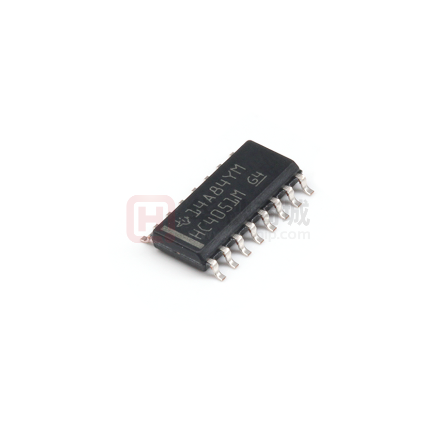


 工商网监
湘ICP备2023018690号
工商网监
湘ICP备2023018690号

