[ /Title
(CD74H
C4066,
CD74H
CT4066
)
/Subject
(HighSpeed
CMOS
Logic
Quad
CD54HC4066, CD74HC4066,
CD74HCT4066
Data sheet acquired from Harris Semiconductor
SCHS208D
High-Speed CMOS Logic
Quad Bilateral Switch
February 1998 - Revised August 2003
Features
Description
• Wide Analog-Input-Voltage Range . . . . . . . . . . 0V - 10V
The ’HC4066 and CD74HCT4066 contain four independent
digitally controlled analog switches that use silicon-gate
CMOS technology to achieve operating speeds similar to
LSTTL with the low power consumption of standard CMOS
integrated circuits.
• Low “ON” Resistance
- VCC = 4.5V. . . . . . . . . . . . . . . . . . . . . . . . . . . . . . . .25Ω
- VCC = 9V . . . . . . . . . . . . . . . . . . . . . . . . . . . . . . . . .15Ω
• Fast Switching and Propagation Delay Times
These switches feature the characteristic linear “ON”
resistance of the metal-gate CD4066B. Each switch is
turned on by a high-level voltage on its control input.
• Low “OFF” Leakage Current
• Wide Operating Temperature Range . . . -55oC to 125oC
Ordering Information
• HC Types
- 2V to 10V Operation
- High Noise Immunity: NIL = 30%, NIH = 30% of VCC
at VCC = 5V and 10V
PART NUMBER
• HCT Types
- Direct LSTTL Input Logic Compatibility,
VIL= 0.8V (Max), VIH = 2V (Min)
- CMOS Input Compatibility, Il ≤ 1µA at VOL, VOH
TEMP. RANGE
(oC)
PACKAGE
CD54HC4066F3A
-55 to 125
14 Ld CERDIP
CD74HC4066E
-55 to 125
14 Ld PDIP
CD74HC4066M
-55 to 125
14 Ld SOIC
CD74HC4066MT
-55 to 125
14 Ld SOIC
CD74HC4066M96
-55 to 125
14 Ld SOIC
CD74HC4066PW
-55 to 125
14 Ld TSSOP
CD74HC4066PWR
-55 to 125
14 Ld TSSOP
CD74HC4066PWT
-55 to 125
14 Ld TSSOP
CD74HCT4066E
-55 to 125
14 Ld PDIP
CD74HCT4066M
-55 to 125
14 Ld SOIC
CD74HCT4066MT
-55 to 125
14 Ld SOIC
CD74HCT4066M96
-55 to 125
14 Ld SOIC
NOTE: When ordering, use the entire part number. The suffixes 96
and R denote tape and reel. The suffix T denotes a small-quantity
reel of 250.
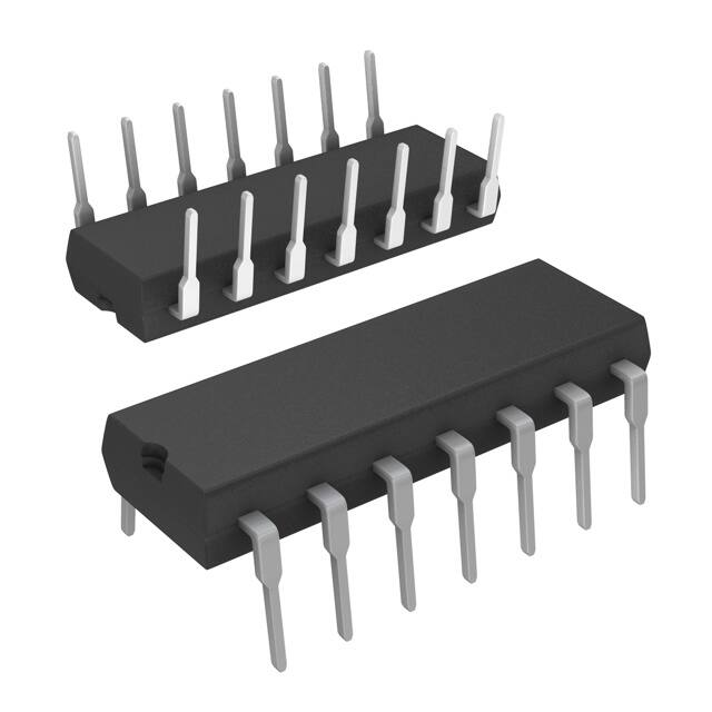
Pinout
CD54HC4066 (CERDIP)
CD74HC4066 (PDIP, SOIC, TSSOP)
CD74HCT4066 (PDIP, SOIC)
TOP VIEW
1Y 1
14 VCC
1Z 2
13 1E
2Z 3
12 4E
2Y 4
11 4Y
2E 5
10 4Z
3E 6
9 3Z
GND 7
8 3Y
CAUTION: These devices are sensitive to electrostatic discharge. Users should follow proper IC Handling Procedures.
Copyright
© 2003, Texas Instruments Incorporated
1
�CD54HC4066, CD74HC4066, CD74HCT4066
Functional Diagram
13
1
1E
2
5
4
2E
3
6
8
3E
9
12
11
4E
10
1Y
1Z
2Y
2Z
3Y
3Z
4Y
4Z
GND = 7
VCC = 14
TRUTH TABLE
INPUT
nE
SWITCH
L
Off
H
On
H= High Level
L= Low Level
Logic Diagram
nY
p
p
n
nZ
n
nE
2
�CD54HC4066, CD74HC4066, CD74HCT4066
Absolute Maximum Ratings
Thermal Information
DC Supply Voltage, VCC
HCT Types . . . . . . . . . . . . . . . . . . . . . . . . . . . . . . . . . -0.5V to 7V
HC Types . . . . . . . . . . . . . . . . . . . . . . . . . . . . . . . . -0.5V to 10.5V
DC Input Diode Current, IIK
For VI < -0.5V or VI > VCC + 0.5V . . . . . . . . . . . . . . . . . . . . . .±20mA
DC Switch Current, IO (Note 1)
For -0.5V < VO < VCC + 0.5V. . . . . . . . . . . . . . . . . . . . . . . . . .±25mA
DC Output Diode Current, IOK
For VO < -0.5V or VO > VCC + 0.5V . . . . . . . . . . . . . . . . . . . .±20mA
DC Output Source or Sink Current per Output Pin, IO
For VO > -0.5V or VO < VCC + 0.5V . . . . . . . . . . . . . . . . . . . .±25mA
DC VCC or Ground Current, ICC . . . . . . . . . . . . . . . . . . . . . . . . .±50mA
Thermal Resistance (Typical, Note 2)
θJA
E (PDIP) Package . . . . . . . . . . . . . . . . . . . . . . . . . .
80oC/W
M (SOIC) Package. . . . . . . . . . . . . . . . . . . . . . . . . .
86oC/W
PW (TSSOP) Package . . . . . . . . . . . . . . . . . . . . . .
113oC/W
Maximum Junction Temperature (Hermetic Package or Die) . . . 175oC
Maximum Junction Temperature (Plastic Package) . . . . . . . . 150oC
Maximum Storage Temperature Range . . . . . . . . . .-65oC to 150oC
Maximum Lead Temperature (Soldering 10s) . . . . . . . . . . . . . 300oC
(SOIC - Lead Tips Only)
Operating Conditions
Temperature Range, TA . . . . . . . . . . . . . . . . . . . . . . -55oC to 125oC
Supply Voltage Range, VCC
HC Types . . . . . . . . . . . . . . . . . . . . . . . . . . . . . . . . . . . .2V to 10V
HCT Types . . . . . . . . . . . . . . . . . . . . . . . . . . . . . . . . .4.5V to 5.5V
DC Input or Output Voltage, VI, VO . . . . . . . . . . . . . . . . . 0V to VCC
Input Rise and Fall Time
2V . . . . . . . . . . . . . . . . . . . . . . . . . . . . . . . . . . . . . . 1000ns (Max)
4.5V. . . . . . . . . . . . . . . . . . . . . . . . . . . . . . . . . . . . . . 500ns (Max)
6V . . . . . . . . . . . . . . . . . . . . . . . . . . . . . . . . . . . . . . . 400ns (Max)
CAUTION: Stresses above those listed in “Absolute Maximum Ratings” may cause permanent damage to the device. This is a stress only rating and operation
of the device at these or any other conditions above those indicated in the operational sections of this specification is not implied.
NOTES:
1. In certain applications, the external load-resistor current may include both VCC and signal-line components. To avoid drawing VCC current
when switch current flows into the transmission gate inputs, (terminals 1, 4, 8 and 11) the voltage drop across the bidirectional switch
must not exceed 0.6V (calculated from RON values shown in the DC Electrical Specifications Table). No VCC current will flow through
RLif the switch current flows into terminals 2, 3, 9 and 10.
2. The package thermal impedance is calculated in accordance with JESD 51-7.
DC Electrical Specifications
TEST
CONDITIONS
PARAMETER
25oC
-40oC TO 85oC
-55oC TO 125oC
SYMBOL
VI (V)
VIS (V)
VCC (V)
MIN
TYP
MAX
MIN
MAX
MIN
MAX
UNITS
VIH
-
-
2
1.5
-
-
1.5
-
1.5
-
V
4.5
3.15
-
-
3.15
-
3.15
-
V
9
6.3
-
-
6.3
-
6.3
-
V
2
-
-
0.5
-
0.5
-
0.5
V
4.5
-
-
1.35
-
1.35
-
1.35
V
9
-
-
2.7
-
2.7
-
2.7
V
HC TYPES
High Level Input
Voltage
Low Level Input
Voltage
VIL
-
-
Input Leakage
Current
(Any Control)
IIL
VCC or
GND
-
10
-
-
±0.1
-
±1
-
±1
µA
Off-Switch Leakage
Current
IZ
VIL
VCC or
GND
10
-
-
±0.1
-
±1
-
±1
µA
3
�CD54HC4066, CD74HC4066, CD74HCT4066
DC Electrical Specifications
(Continued)
TEST
CONDITIONS
PARAMETER
“ON” Resistance
IO = 1mA
(Figure 1)
Quiescent Device
Current
-40oC TO 85oC
-55oC TO 125oC
SYMBOL
VI (V)
VIS (V)
VCC (V)
MIN
TYP
MAX
MIN
MAX
MIN
MAX
UNITS
RON
VCC
VCC or
GND
4.5
-
25
80
-
106
-
128
Ω
6
-
20
75
-
94
-
113
Ω
9
-
15
60
-
78
-
95
Ω
4.5
-
35
95
-
118
-
142
Ω
6
-
24
84
-
105
-
126
Ω
9
-
16
70
-
88
-
105
Ω
4.5
-
1
-
-
-
-
-
Ω
6
-
0.75
-
-
-
-
-
Ω
9
-
0.5
-
-
-
-
-
Ω
VCC to
GND
“ON” Resistance
Between Any Two
Switches
25oC
∆RON
ICC
VCC
-
VCC or
GND
-
6
-
-
2
-
20
-
40
µA
10
-
-
16
-
160
-
320
µA
HCT TYPES
High Level Input
Voltage
VIH
-
-
4.5 to
5.5
2
-
-
2
-
2
-
V
Low Level Input
Voltage
VIL
-
-
4.5 to
5.5
-
-
0.8
-
0.8
-
0.8
V
Input Leakage
Current
(Any Control)
IIL
VCC or
GND
-
5.5
-
-
±0.1
-
±1
-
±1
µA
Off-Switch Leakage
Current
IZ
VIL
VCC or
GND
5.5
-
-
±0.1
-
±1
-
±1
µA
RON
VCC
VCC or
GND
4.5
-
25
80
-
106
-
128
Ω
VCC to
GND
4.5
-
35
95
-
118
-
142
Ω
“ON” Resistance
IO = 1mA
(Figure 1)
“ON” Resistance
Between Any Two
Switches
∆RON
VCC
-
4.5
-
1
-
-
-
-
-
Ω
Quiescent Device
Current
ICC
VCC or
GND
-
5.5
-
-
2
-
20
-
40
µA
∆ICC
(Note 3)
VCC
- 2.1
-
4.5 to
5.5
-
100
360
-
450
-
490
µA
Additional Quiescent
Device Current Per
Input Pin: 1 Unit Load
NOTE:
3. For dual-supply systems theoretical worst case (VI = 2.4V, VCC = 5.5V) specification is 1.8mA.
HCT Input Loading Table
INPUT
UNIT LOADS
All
1
NOTE: Unit Load is ∆ICC limit specified in DC Electrical Specifications table, e.g., 360µA max at 25oC.
4
�CD54HC4066, CD74HC4066, CD74HCT4066
Switching Specifications Input tr, tf = 6ns
PARAMETER
SYMBOL
TEST
CONDITIONS
tPLH, tPHL
CL = 50pF
VCC
(V)
25oC
MIN
TYP
-40oC TO 85oC -55oC TO 125oC
MAX
MIN
MAX
MIN
MAX
UNITS
HC TYPES
Propagation Delay Time
Switch In to Out
Propagation Delay Time
Switch Turn On Delay
tPZH, tPZL
2
-
-
60
-
75
-
90
ns
4.5
-
-
12
-
15
-
18
ns
9
-
-
8
-
11
-
13
ns
CL = 15pF
5
-
4
-
-
-
-
-
ns
CL = 50pF
2
-
-
100
-
125
-
150
ns
4.5
-
-
20
-
25
-
30
ns
9
-
-
12
-
15
-
18
ns
5
-
8
-
-
-
-
-
ns
CL = 15pF
Propagation Delay Time
Switch Turn Off Delay
2
-
-
150
-
190
-
225
ns
4.5
-
-
30
-
38
-
45
ns
9
-
-
24
-
30
-
36
ns
CL = 15pF
5
-
12
-
-
-
-
-
ns
CI
-
-
-
-
10
-
10
-
10
pF
CPD
-
5
-
25
-
-
-
-
-
pF
Propagation Delay Time
Switch In to Out
tPLH, tPHL
CL = 50pF
4.5
-
-
12
-
15
-
18
ns
CL = 15pF
5
-
4
-
-
-
-
-
ns
Propagation Delay Time
Switch Turn On Delay
tPZH, tPZL
CL = 50pF
4.5
-
-
24
-
30
-
36
ns
CL = 15pF
5
-
9
-
-
-
-
-
ns
Propagation Delay Time
Switch Turn Off Delay
tPHZ, tPLZ
CL = 50pF
4.5
-
-
35
-
44
-
53
ns
Input (Control) Capacitance
Power Dissipation Capacitance
(Notes 4, 5)
tPHZ, tPLZ
CL = 50pF
HCT TYPES
Input (Control) Capacitance
Power Dissipation Capacitance
(Notes 4, 5)
CL = 15pF
5
-
14
-
-
-
-
-
ns
CI
-
-
-
-
10
-
10
-
10
pF
CPD
-
5
-
38
-
-
-
-
-
pF
NOTES:
4. CPD is used to determine the dynamic power consumption, per package.
5. PD = CPD VCC2 fi + Σ (CL + CS) VCC2 fo where fi = input frequency, fo = output frequency, CL = output load capacitance, CS = switch
capacitance, VCC = supply voltage.
Analog Channel Specifications
TA = 25oC
PARAMETER
TEST CONDITIONS
VCC (V)
HC4066
CD74HCT4066
UNITS
Switch Frequency Response Bandwidth at -3dB
Figure 2
Figure 5, Notes 6, 7
4.5
200
200
MHz
Cross Talk Between Any Two Switches Figure 3
Figure 4, Notes 7, 8
4.5
-72
-72
dB
Total Harmonic Distortion
Figure 6, 1kHz,
VIS = 4VP-P
4.5
0.022
0.023
%
Figure 6, 1kHz,
VIS = 8VP-P
9
0.008
N/A
%
5
�CD54HC4066, CD74HC4066, CD74HCT4066
TA = 25oC (Continued)
Analog Channel Specifications
PARAMETER
TEST CONDITIONS
Control to Switch Feedthrough Noise
VCC (V)
HC4066
CD74HCT4066
UNITS
4.5
200
130
mV
9
550
N/A
mV
4.5
-72
-72
dB
-
5
5
pF
Figure 7
Switch “OFF” Signal Feedthrough Figure 3
Figure 8, Notes 7, 8
Switch Input Capacitance, CS
NOTES:
6. Adjust input level for 0dBm at output, f = 1MHz.
7. VIS is centered at VCC/2.
8. Adjust input for 0dBm at VIS.
Typical Performance Curves
“ON” RESISTANCE, RON (Ω)
40
CHANNEL-ON BANDWIDTH, dB
TA = 25oC, GND = 0V
50
VCC = 4.5V, PIN 1 TO 2
30
20
VCC = 9V, PIN 1 TO 3
10
0
0
1
2
3
4 4.5 5
6
7
8
9
CROSSTALK, dB
SWITCH-OFF SIGNAL FEEDTHROUGH, dB
-2
CL = 10pF
VCC = 4.5V
RL = 50Ω
TA = 25oC
PIN 4 TO 3
-3
105
106
107
FIGURE 2. SWITCH FREQUENCY RESPONSE, VCC = 4.5V
CL = 10pF
VCC = 4.5V
RL = 50Ω
TA = 25oC
PIN 4 TO 3
-40
-60
-80
-100
104
108
FREQUENCY, f (Hz)
FIGURE 1. TYPICAL “ON” RESISTANCE vs INPUT SIGNAL
VOLTAGE
-20
-1
-4
104
10
INPUT SIGNAL VOLTAGE, VIS (V)
0
0
105
106
107
108
FREQUENCY, f (Hz)
FIGURE 3. SWITCH-OFF SIGNAL FEEDTHROUGH AND CROSSTALK vs FREQUENCY, VCC = 4.5V
6
�CD54HC4066, CD74HC4066, CD74HCT4066
Analog Test Circuits
VIS
0.1µF
VCC
VCC
SWITCH
ON
VIS
R
VOS1
R
R
C
VOS2
SWITCH
OFF
R
VCC/2
VCC/2
C
dB
METER
VCC/2
fIS = 1MHz SINEWAVE
R = 50Ω
C = 10pF
FIGURE 4. CROSSTALK BETWEEN TWO SWITCHES TEST CIRCUIT
VCC
VCC
0.1µF
VIS
SINE
WAVE 10µF
VIS
VOS
SWITCH
ON
50Ω
VIS
VI = VIH
SWITCH
ON
VOS
10kΩ
10pF
dB
METER
VCC/2
50pF
DISTORTION
METER
VCC/2
fIS = 1kHz TO 10kHz
FIGURE 5. FREQUENCY RESPONSE TEST CIRCUIT
E
VCC
600Ω
VCC/2
FIGURE 6. TOTAL HARMONIC DISTORTION TEST CIRCUIT
SWITCH
ALTERNATING
ON AND OFF
tr, tf ≤ 6ns
fCONT = 1MHz
50% DUTY
CYCLE
VCC
VC = VIL
VP-P
VOS
0.1µF
VOS
50pF
SCOPE
VCC/2
FIGURE 7. CONTROL-TO-SWITCH FEEDTHROUGH NOISE
TEST CIRCUIT
VOS
SWITCH
OFF
VIS
600Ω
fIS ≥ 1MHz SINEWAVE
R = 50Ω
C = 10pF
R
R
VCC/2
VCC/2
C
dB
METER
FIGURE 8. SWITCH OFF SIGNAL FEEDTHROUGH
Test Circuits and Waveforms
tr = 6ns
tf = 6ns
90%
50%
10%
INPUT
GND
tTLH
GND
tTHL
90%
50%
10%
INVERTING
OUTPUT
3V
2.7V
1.3V
0.3V
INPUT
tTHL
tPHL
tf = 6ns
tr = 6ns
VCC
tTLH
90%
1.3V
10%
INVERTING
OUTPUT
tPHL
tPLH
FIGURE 9. HC TRANSITION TIMES AND PROPAGATION
DELAY TIMES, COMBINATION LOGIC
tPLH
FIGURE 10. HCT TRANSITION TIMES AND PROPAGATION
DELAY TIMES, COMBINATION LOGIC
7
�PACKAGE OPTION ADDENDUM
www.ti.com
14-Oct-2022
PACKAGING INFORMATION
Orderable Device
Status
(1)
Package Type Package Pins Package
Drawing
Qty
Eco Plan
(2)
Lead finish/
Ball material
MSL Peak Temp
Op Temp (°C)
Device Marking
(3)
Samples
(4/5)
(6)
5962-8950701CA
ACTIVE
CDIP
J
14
1
Non-RoHS
& Green
SNPB
N / A for Pkg Type
-55 to 125
5962-8950701CA
CD54HC4066F3A
Samples
CD54HC4066F3A
ACTIVE
CDIP
J
14
1
Non-RoHS
& Green
SNPB
N / A for Pkg Type
-55 to 125
5962-8950701CA
CD54HC4066F3A
Samples
CD74HC4066E
ACTIVE
PDIP
N
14
25
RoHS & Green
NIPDAU
N / A for Pkg Type
-55 to 125
CD74HC4066E
Samples
CD74HC4066EE4
ACTIVE
PDIP
N
14
25
RoHS & Green
NIPDAU
N / A for Pkg Type
-55 to 125
CD74HC4066E
Samples
CD74HC4066M
ACTIVE
SOIC
D
14
50
RoHS & Green
NIPDAU
Level-1-260C-UNLIM
-55 to 125
HC4066M
Samples
CD74HC4066M96
ACTIVE
SOIC
D
14
2500
RoHS & Green
NIPDAU
Level-1-260C-UNLIM
-55 to 125
HC4066M
Samples
CD74HC4066M96E4
ACTIVE
SOIC
D
14
2500
RoHS & Green
NIPDAU
Level-1-260C-UNLIM
-55 to 125
HC4066M
Samples
CD74HC4066ME4
ACTIVE
SOIC
D
14
50
RoHS & Green
NIPDAU
Level-1-260C-UNLIM
-55 to 125
HC4066M
Samples
CD74HC4066MG4
ACTIVE
SOIC
D
14
50
RoHS & Green
NIPDAU
Level-1-260C-UNLIM
-55 to 125
HC4066M
Samples
CD74HC4066MT
ACTIVE
SOIC
D
14
250
RoHS & Green
NIPDAU
Level-1-260C-UNLIM
-55 to 125
HC4066M
Samples
CD74HC4066PW
ACTIVE
TSSOP
PW
14
90
RoHS & Green
NIPDAU
Level-1-260C-UNLIM
-55 to 125
HP4066
Samples
CD74HC4066PWR
ACTIVE
TSSOP
PW
14
2000
RoHS & Green
NIPDAU
Level-1-260C-UNLIM
-55 to 125
HP4066
Samples
CD74HC4066PWT
ACTIVE
TSSOP
PW
14
250
RoHS & Green
NIPDAU
Level-1-260C-UNLIM
-55 to 125
HP4066
Samples
CD74HCT4066E
ACTIVE
PDIP
N
14
25
RoHS & Green
NIPDAU
N / A for Pkg Type
-55 to 125
CD74HCT4066E
Samples
CD74HCT4066M
ACTIVE
SOIC
D
14
50
RoHS & Green
NIPDAU
Level-1-260C-UNLIM
-55 to 125
HCT4066M
Samples
CD74HCT4066M96
ACTIVE
SOIC
D
14
2500
RoHS & Green
NIPDAU
Level-1-260C-UNLIM
-55 to 125
HCT4066M
Samples
CD74HCT4066MT
ACTIVE
SOIC
D
14
250
RoHS & Green
NIPDAU
Level-1-260C-UNLIM
-55 to 125
HCT4066M
Samples
(1)
The marketing status values are defined as follows:
ACTIVE: Product device recommended for new designs.
LIFEBUY: TI has announced that the device will be discontinued, and a lifetime-buy period is in effect.
NRND: Not recommended for new designs. Device is in production to support existing customers, but TI does not recommend using this part in a new design.
Addendum-Page 1
�PACKAGE OPTION ADDENDUM
www.ti.com
14-Oct-2022
PREVIEW: Device has been announced but is not in production. Samples may or may not be available.
OBSOLETE: TI has discontinued the production of the device.
(2)
RoHS: TI defines "RoHS" to mean semiconductor products that are compliant with the current EU RoHS requirements for all 10 RoHS substances, including the requirement that RoHS substance
do not exceed 0.1% by weight in homogeneous materials. Where designed to be soldered at high temperatures, "RoHS" products are suitable for use in specified lead-free processes. TI may
reference these types of products as "Pb-Free".
RoHS Exempt: TI defines "RoHS Exempt" to mean products that contain lead but are compliant with EU RoHS pursuant to a specific EU RoHS exemption.
Green: TI defines "Green" to mean the content of Chlorine (Cl) and Bromine (Br) based flame retardants meet JS709B low halogen requirements of


 工商网监
湘ICP备2023018690号
工商网监
湘ICP备2023018690号
