CDC421xxx
www.ti.com
SLAS540 – APRIL 2007
FULLY INTEGRATED FIXED FREQUENCY LOW-JITTER, CRYSTAL-OSCILLATOR CLOCK
GENERATOR
•
FEATURES
•
•
•
•
•
Single 3.3 V Supply
High-Performance Clock Generator,
Incorporating Crystal Oscillator Circuitry With
Integrated Frequency Synthesizer
Low Output Jitter, as Low as 380 fs (rms
integrated between 10 kHz–20 MHz)
Low Phase Noise at 312.5 MHz, Less Than
–120 dBc/Hz at 10 kHz and –147 dBc/Hz at 10
MHz Offset From the Carrier
Supports Crystal Frequencies or LVCMOS
Input Frequencies at 31.25 MHz, 33.33 MHz,
and 35.42 MHz
•
•
•
•
•
•
•
Output Frequencies: 100 MHz, 106.25 MHz,
125 MHz, 156.25 MHz, 212.5 MHz, 250 MHz,
and 312.5 MHz
Differential Low-Voltage Positive Emitter
Coupled Logic (LVPECL) Output
Fully Integrated Voltage-Controlled Oscillator
(VCO) Running from 1.75 GHz to 2.35 GHz
Typical Power Consumption 300 mW
Chip-Enable Control Pin
QFN-24 Package
ESD Protection Exceeds 2 kV HBM
Industrial Temperature Range –40°C to 85°C
A
APPLICATIONS
A
•
A
Low-Cost, Low-Jitter Frequency Multiplier
A
External Crystal
LVPECL
VCO
Output Divider
Feedback
Divider
CLK
Prescaler
Crystal
Oscillator
Input
PFD/Charge Pump
Loop Filter
NCLK
B0216-02
DESCRIPTION
CDC421xxx is a high-performance, low-phase-noise clock generator. It has an integrated low-noise, LC-based
voltage-controlled oscillator (VCO) that operates within the 1.75 GHz–2.35 GHz frequency range. It has an
integrated crystal oscillator that operates in conjunction with an external AT-cut crystal to produce a stable
frequency reference for the PLL-based frequency synthesizer. The output frequency (fout) is proportional to the
frequency of the input crystal (fxtal).
The device operates in a 3.3 V supply environment and is characterized for operation from –40°C to 85°C.
CDC421xxx is available in a QFN-24 package.
A high-level block diagram of the CDC421xxx is shown in Figure 1.
Please be aware that an important notice concerning availability, standard warranty, and use in critical applications of Texas
Instruments semiconductor products and disclaimers thereto appears at the end of this data sheet.
PRODUCTION DATA information is current as of publication date.
Products conform to specifications per the terms of the Texas
Instruments standard warranty. Production processing does not
necessarily include testing of all parameters.
Copyright © 2007, Texas Instruments Incorporated
�CDC421xxx
www.ti.com
SLAS540 – APRIL 2007
XIN 1
XIN 2
Crystal
Oscillator
Loop Filter
PFD/
Charge Pump
VCO
Prescaler
Output
Divider
Feedback
Divider
B0230-01
Figure 1. High-Level Block Diagram of the CDC421xxx
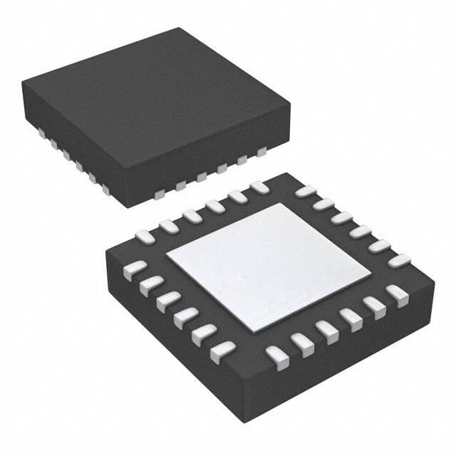
PACKAGE (QFN-24)
The CDC421xxx is packaged in a QFN-24 terminal package. The QFN package footprint is shown. Terminal
locations and numbers are shown in Figure 2.
NC
NC
XIN2
XIN 1
NC
NC
24
23
22
21
20
19
RGE PACKAGE
(TOP VIEW)
CE
1
18
NC
NC
2
17
VCC
NC
3
16
VCC
CDC421xxx
12
NC
NC
13
11
6
NC
NC
10
NC
OUTP
14
9
5
GND
NC
8
NC
GND
15
7
4
OUTN
NC
P0024-06
Figure 2. Pinout of the CDC421xxx QFN-24 Package
The terminal functions table shows the terminal descriptions for the CDC421xxx QFN-24 package.
Table 1. TERMINAL FUNCTIONS
TERMINAL
NAME
2
NO.
TYPE
ESD
PROTECTION
DESCRIPTION
VCC
16, 17
Power
Y
3.3V power supply
GND
8, 9
GND
Y
Ground
XIN 1
XIN 2
21
22
I
I
Y
N
In crystal input mode, connect XIN1 to one end of the crystal and XIN2 to the
other end of the crystal. In LVCMOS single-ended driven mode, XIN1 (pin 21) acts
as input reference and XIN2 should connect to GND.
Submit Documentation Feedback
�CDC421xxx
www.ti.com
SLAS540 – APRIL 2007
Table 1. TERMINAL FUNCTIONS (continued)
TERMINAL
NAME
NO.
TYPE
ESD
PROTECTION
DESCRIPTION
CE
1
I
Y
Chip enable (LVCMOS input)
CE = 1 enables the device and the outputs.
CE = 0 disables all current sources (LVPECLP = LVPECLN = Hi-Z).
OUTP
10
O
Y
High-speed positive differential LVPECL output. (Outputs are enabled by CE )
OUTN
7
O
Y
High-speed negative differential LVPECL output. (Outputs are enabled by CE )
2–6, 11–15,
18–20, 23,
24
I or O
Y
TI test pin. Do not connect; leave floating.
NC
DEVICE SELECTION
The CDC421xxx device is an LVPECL low-phase-noise clock generator designed to work with a low-frequency
AT-crystal oscillator of a single-ended LVCMOS.
Table 2. Device Selection Table for CDC421xxx
CDC421xxx
INPUT FREQUENCY OR
CRYSTAL VALUE (MHz)
OUTPUT FREQUENCY FOR
THE SPECIFIED INPUT
FREQUENCY (MHz)
QFN-24 tape and reel
33.3333
100.00
QFN-24 small tape and reel
33.3333
100.00
CDC421106RGER
QFN-24 tape and reel
35.4167
106.25
421106
CDC421106RGET
QFN-24 small tape and reel
35.4167
106.25
421125
CDC421125RGER
QFN-24 tape and reel
31.2500
125.00
421125
CDC421125RGET
QFN-24 small tape and reel
31.2500
125.00
421156
CDC421156RGER
QFN-24 tape and reel
31.2500
156.25
421156
CDC421156RGET
QFN-24 small tape and reel
31.2500
156.25
421212
CDC421212RGER
QFN-24 tape and reel
35.4167
212.50
421212
CDC421212RGET
QFN-24 small tape and reel
35.4167
212.50
421250
CDC421250RGER
QFN-24 tape and reel
31.2500
250.00
421250
CDC421250RGET
QFN-24 small tape and reel
31.2500
250.00
421312
CDC421312RGER
QFN-24 tape and reel
31.2500
312.50
421312
CDC421312RGET
QFN-24 small tape and reel
31.2500
312.50
DEVICE
MARKING
ORDERING
PART NUMBER
421100
CDC421100RGER
421100
CDC421100RGET
421106
PACKAGE
ABSOLUTE MAXIMUM RATINGS
over operating free-air temperature range (unless otherwise noted) (1)
VALUE
UNIT
–0.5 to 4.6
V
–0.5 to VCC + 0.5
V
Output current for LVPECL
–50
mA
Electrostatic discharge (HBM)
2k
V
–40 to 85
°C
125
°C
–65 to 150
°C
VCC
Supply voltage (2)
VI
Voltage range for all other input pins (2)
IO
TA
Characterized free-air temperature range (no airflow)
TJ
Maximum junction temperature
Tstg
Storage temperature range
(1)
(2)
Stresses beyond those listed under absolute maximum ratings may cause permanent damage to the device. These are stress ratings
only, and functional operation of the device at these or any other conditions beyond those indicated under recommended operating
conditions is not implied. Exposure to absolute-maximum rated conditions for extended periods may affect device reliability.
All voltage values are with respect to network ground terminal.
Submit Documentation Feedback
3
�CDC421xxx
www.ti.com
SLAS540 – APRIL 2007
RECOMMENDED OPERATING CONDITIONS
over operating free-air temperature range (unless otherwise noted)
VCC
Supply voltage
TA
Ambient temperature, no airflow, no heat sink
MIN
NOM
MAX
3
3.3
3.6
V
85
°C
–40
UNIT
ELECTRICAL CHARACTERISTICS
over recommended operating conditions for CDC421xxx device
PARAMETER
VCC
Supply voltage
IVCC
Total current at 3.3 V
TEST CONDITIONS
MIN
TYP
3
3.3
3.6
V
91
110
mA
MHz
3.3 V, 312.5 MHz
MAX
UNIT
LVPECL OUTPUT
fCLK
Output frequency
100
312.5
VOH
LVPECL high-level output voltage
VCC – 1.20
VCC – 0.81
VOL
LVPECL low-level output voltage
VCC – 2.17
VCC – 1.36
|VOD|
LVPECL differential output voltage
407
1076
tr
Output rise time
20% to 80% of VOUTpp
170
tf
Output fall time
80% to 20% of VOUTpp
170
Duty cycle of the output waveform
45%
V
V
mV
ps
ps
55%
LVCMOS INPUT
4
VIL,CMOS
Low-level CMOS input voltage
VCC = 3.3 V
VIH,CMOS
High-level CMOS input voltage
VCC = 3.3 V
IL,CMOS
Low-level CMOS input current
VCC = VCC max, VIL = 0 V
IH,CMOS
High-level CMOS input current
VCC = VCC min, VIH = 3.7 V
Submit Documentation Feedback
0.3 VCC
0.7 VCC
V
V
–200
µA
200
µA
�CDC421xxx
www.ti.com
SLAS540 – APRIL 2007
JITTER CHARACTERISTICS IN INPUT CLOCK MODE
The jitter characterization test is performed using an LVCMOS input signal driving the CDC421xxx device.
0.1 mF
Phase Noise
Analyzer
XIN 1
50 W
100 pF
CDC421xxx
XIN 2
150 W
150 W
150 W
S0246-02
Figure 3. Jitter Test Configuration for an LVTTL Input Driving CDC421xxx
For the cases of the CDC421xxx being referenced by an external, clean LVCMOS input of 31.25 MHz, 33.33
MHz and 35.4167 MHz, the following tables list the measured SSB phase noise of all the outputs supported by
the CDC421xxx device, (100 MHz, 106.25 MHz, 125 MHz, 156.25 MHz, 212.5 MHz, 250 MHz, and 312.5 MHz)
from 100 Hz to 20 MHz from the carrier.
Table 3. Phase Noise Parameters With LVCMOS Input of 33.3333 MHz and LVPECL Output at 100.00 MHz
PARAMETER
MIN
TYP
MAX
UNIT
Phase Noise Specifications Under Following Conditions: fin = 33.3333 MHz, fout = 100.00 MHz
phn100
Phase noise at 100 Hz
–111
dBc/Hz
phn1K
Phase noise at 1 kHz
–121
dBc/Hz
phn10k
Phase noise at 10 kHz
–131
dBc/Hz
phn100k
Phase noise at 100 kHz
–133
dBc/Hz
phn1M
Phase Noise at 1 MHz
–142
dBc/Hz
phn10M
Phase noise at 10 MHz
–149
dBc/Hz
phn20M
Phase noise at 20 MHz
–149
dBc/Hz
JRMS
RMS jitter integrated from 12 kHz to 20 MHz
507
fs
Tj
Total jitter
35.33
ps
Dj
Deterministic jitter
11.54
ps
Table 4. Phase Noise Parameters With LVCMOS Input of 35.4167 MHz and LVPECL Output at 106.25 MHz
PARAMETER
MIN
TYP
MAX
UNIT
Phase Noise Specifications Under Following Conditions: fin= 35.4167 MHz , fout = 106.25 MHz
phn100
Phase noise at 100 Hz
–112
dBc/Hz
phn1K
Phase noise at 1 kHz
–121
dBc/Hz
phn10k
Phase noise at 10 kHz
–125
dBc/Hz
phn100k
Phase noise at 100 kHz
–129
dBc/Hz
phn1M
Phase noise at 1 MHz
–142
dBc/Hz
phn10M
Phase noise at 10 MHz
–151
dBc/Hz
phn20M
Phase noise at 20 MHz
–151
dBc/Hz
JRMS
RMS jitter integrated from 12 kHz to 20 MHz
Tj
Total jitter
Dj
Deterministic jitter
Submit Documentation Feedback
530
fs
30.39
ps
11
ps
5
�CDC421xxx
www.ti.com
SLAS540 – APRIL 2007
Table 5. Phase Noise Parameters With LVCMOS Input of 31.2500 MHz and LVPECL Output at 125.00 MHz
PARAMETER
MIN
TYP
MAX
UNIT
Phase Noise Specifications Under Following Conditions: fin = 31.2500 MHz, fout = 125.00 MHz
phn100
Phase noise at 100 Hz
–108
dBc/Hz
phn1K
Phase noise at 1 kHz
–118
dBc/Hz
phn10k
Phase noise at 10 kHz
–127
dBc/Hz
phn100k
Phase noise at 100 kHz
–130
dBc/Hz
phn1M
Phase noise at 1 MHz
–139
dBc/Hz
phn10M
Phase noise at 10 MHz
–147
dBc/Hz
phn20M
Phase noise at 20 MHz
–147
dBc/Hz
JRMS
RMS jitter integrated from 12 kHz to 20 MHz
Tj
Total jitter
Dj
Deterministic jitter
529
fs
47.47
ps
25.2
ps
Table 6. Phase Noise Parameters With LVCMOS Input of 31.2500 MHz and LVPECL Output at 156.25 MHz
PARAMETER
MIN
TYP
MAX
UNIT
Phase Noise Specifications Under Following Conditions: fin = 31.2500 MHz, fout = 156.25 MHz
phn100
Phase noise at 100 Hz
–106
dBc/Hz
phn1K
Phase noise at 1 kHz
–117
dBc/Hz
phn10k
Phase noise at 10 kHz
–126
dBc/Hz
phn100k
Phase noise at 100 kHz
–128
dBc/Hz
phn1M
Phase noise at 1 MHz
–139
dBc/Hz
phn10M
Phase noise at 10 MHz
–147
dBc/Hz
phn20M
Phase noise at 20 MHz
–147
dBc/Hz
JRMS
RMS jitter integrated from 12 kHz to 20 MHz
Tj
Total jitter
Dj
Deterministic jitter
472
fs
31.54
ps
9.12
ps
Table 7. Phase Noise Parameters With LVCMOS Input of 35.4167 MHz and LVPECL Output at 212.50 MHz
PARAMETER
MIN
TYP
MAX
UNIT
Phase Noise Specifications Under Following Conditions: fin = 35.4167 MHz, fout = 212.50 MHz
6
phn100
Phase noise at 100 Hz
–105
dBc/Hz
phn1K
Phase noise at 1 kHz
–115
dBc/Hz
phn10k
Phase noise at 10 kHz
–119
dBc/Hz
phn100k
Phase noise at 100 kHz
–123
dBc/Hz
phn1M
Phase noise at 1 MHz
–135
dBc/Hz
phn10M
Phase noise at 10 MHz
–148
dBc/Hz
phn20M
Phase noise at 20 MHz
–148
dBc/Hz
JRMS
RMS jitter integrated from 12 kHz to 20 MHz
Tj
Dj
512
fs
Total jitter
33.96
ps
Deterministic jitter
13.78
ps
Submit Documentation Feedback
�CDC421xxx
www.ti.com
SLAS540 – APRIL 2007
Table 8. Phase Noise Parameters With LVCMOS Input of 31.2500 MHz and LVPECL Output at 250.00 MHz
PARAMETER
MIN
TYP
MAX
UNIT
Phase Noise Specifications Under Following Conditions: fin = 31.2500 MHz, fout = 250.00 MHz
phn100
Phase noise at 100 Hz
–103
dBc/Hz
phn1K
Phase noise at 1 kHz
–112
dBc/Hz
phn10k
Phase noise at 10 kHz
–121
dBc/Hz
phn100k
Phase noise at 100 kHz
–124
dBc/Hz
phn1M
Phase noise at 1 MHz
–134
dBc/Hz
phn10M
Phase noise at 10 MHz
–148
dBc/Hz
phn20M
Phase noise at 20 MHz
–149
dBc/Hz
JRMS
RMS jitter integrated from 12 kHz to 20 MHz
Tj
Dj
420
fs
Total jitter
36.98
ps
Deterministic jitter
18.52
ps
Table 9. Phase Noise Parameters With LVCMOS Input of 31.2500 MHz and LVPECL Output at 312.50 MHz
PARAMETER
MIN
TYP
MAX
UNIT
Phase Noise Specifications Under Following Conditions: fin = 31.2500 MHz, fout = 312.50 MHz
phn100
Phase noise at 100 Hz
–102
dBc/Hz
phn1K
Phase noise at 1 kHz
–111
dBc/Hz
phn10k
Phase noise at 10 kHz
–120
dBc/Hz
phn100k
Phase noise at 100 kHz
–123
dBc/Hz
phn1M
Phase noise at 1 MHz
–135
dBc/Hz
phn10M
Phase noise at 10 MHz
–147
dBc/Hz
phn20M
Phase noise at 20 MHz
–147
dBc/Hz
JRMS
RMS jitter integrated from 12 kHz to 20 MHz
Tj
Total jitter
Dj
Deterministic jitter
Submit Documentation Feedback
378
fs
29.82
ps
11
ps
7
��IMPORTANT NOTICE
Texas Instruments Incorporated and its subsidiaries (TI) reserve the right to make corrections, enhancements, improvements and other
changes to its semiconductor products and services per JESD46, latest issue, and to discontinue any product or service per JESD48, latest
issue. Buyers should obtain the latest relevant information before placing orders and should verify that such information is current and
complete. All semiconductor products (also referred to herein as “components”) are sold subject to TI’s terms and conditions of sale
supplied at the time of order acknowledgment.
TI warrants performance of its components to the specifications applicable at the time of sale, in accordance with the warranty in TI’s terms
and conditions of sale of semiconductor products. Testing and other quality control techniques are used to the extent TI deems necessary
to support this warranty. Except where mandated by applicable law, testing of all parameters of each component is not necessarily
performed.
TI assumes no liability for applications assistance or the design of Buyers’ products. Buyers are responsible for their products and
applications using TI components. To minimize the risks associated with Buyers’ products and applications, Buyers should provide
adequate design and operating safeguards.
TI does not warrant or represent that any license, either express or implied, is granted under any patent right, copyright, mask work right, or
other intellectual property right relating to any combination, machine, or process in which TI components or services are used. Information
published by TI regarding third-party products or services does not constitute a license to use such products or services or a warranty or
endorsement thereof. Use of such information may require a license from a third party under the patents or other intellectual property of the
third party, or a license from TI under the patents or other intellectual property of TI.
Reproduction of significant portions of TI information in TI data books or data sheets is permissible only if reproduction is without alteration
and is accompanied by all associated warranties, conditions, limitations, and notices. TI is not responsible or liable for such altered
documentation. Information of third parties may be subject to additional restrictions.
Resale of TI components or services with statements different from or beyond the parameters stated by TI for that component or service
voids all express and any implied warranties for the associated TI component or service and is an unfair and deceptive business practice.
TI is not responsible or liable for any such statements.
Buyer acknowledges and agrees that it is solely responsible for compliance with all legal, regulatory and safety-related requirements
concerning its products, and any use of TI components in its applications, notwithstanding any applications-related information or support
that may be provided by TI. Buyer represents and agrees that it has all the necessary expertise to create and implement safeguards which
anticipate dangerous consequences of failures, monitor failures and their consequences, lessen the likelihood of failures that might cause
harm and take appropriate remedial actions. Buyer will fully indemnify TI and its representatives against any damages arising out of the use
of any TI components in safety-critical applications.
In some cases, TI components may be promoted specifically to facilitate safety-related applications. With such components, TI’s goal is to
help enable customers to design and create their own end-product solutions that meet applicable functional safety standards and
requirements. Nonetheless, such components are subject to these terms.
No TI components are authorized for use in FDA Class III (or similar life-critical medical equipment) unless authorized officers of the parties
have executed a special agreement specifically governing such use.
Only those TI components which TI has specifically designated as military grade or “enhanced plastic” are designed and intended for use in
military/aerospace applications or environments. Buyer acknowledges and agrees that any military or aerospace use of TI components
which have not been so designated is solely at the Buyer's risk, and that Buyer is solely responsible for compliance with all legal and
regulatory requirements in connection with such use.
TI has specifically designated certain components as meeting ISO/TS16949 requirements, mainly for automotive use. In any case of use of
non-designated products, TI will not be responsible for any failure to meet ISO/TS16949.
Products
Applications
Audio
www.ti.com/audio
Automotive and Transportation
www.ti.com/automotive
Amplifiers
amplifier.ti.com
Communications and Telecom
www.ti.com/communications
Data Converters
dataconverter.ti.com
Computers and Peripherals
www.ti.com/computers
DLP® Products
www.dlp.com
Consumer Electronics
www.ti.com/consumer-apps
DSP
dsp.ti.com
Energy and Lighting
www.ti.com/energy
Clocks and Timers
www.ti.com/clocks
Industrial
www.ti.com/industrial
Interface
interface.ti.com
Medical
www.ti.com/medical
Logic
logic.ti.com
Security
www.ti.com/security
Power Mgmt
power.ti.com
Space, Avionics and Defense
www.ti.com/space-avionics-defense
Microcontrollers
microcontroller.ti.com
Video and Imaging
www.ti.com/video
RFID
www.ti-rfid.com
OMAP Applications Processors
www.ti.com/omap
TI E2E Community
e2e.ti.com
Wireless Connectivity
www.ti.com/wirelessconnectivity
Mailing Address: Texas Instruments, Post Office Box 655303, Dallas, Texas 75265
Copyright © 2016, Texas Instruments Incorporated
�


 工商网监
湘ICP备2023018690号
工商网监
湘ICP备2023018690号
