Product
Folder
Sample &
Buy
Support &
Community
Tools &
Software
Technical
Documents
Reference
Design
CDCE62005
SCAS862G – NOVEMBER 2008 – REVISED JULY 2016
CDCE62005 3:5 Clock Generator, Jitter Cleaner with Integrated Dual VCOs
1 Features
3 Description
•
The CDCE62005 is a high performance clock
generator and distributor featuring low output jitter, a
high degree of configurability via a SPI interface, and
programmable start up modes determined by on-chip
EEPROM. Specifically tailored for clocking data
converters and high-speed digital signals, the
CDCE62005 achieves jitter performance well under 1
ps RMS (10 kHz to 20 MHz integration bandwidth).
1
•
•
•
•
Superior Performance:
– Low Noise Clock Generator: 550 fs rms typical
(10 kHz to 20 MHz Integration Bandwidth),
FC = 100 MHz
– Low Noise Jitter Cleaner: 2.6 ps rms typical
(10 kHz to 20 MHz Integration Bandwidth),
FC = 100 MHz
Flexible Frequency Planning:
– 5 Fully Configurable Outputs: LVPECL, LVDS,
LVCMOS and Special High Swing Output
Modes
– Unique Dual-VCO Architecture Supports a
Wide Tuning Range: 1.750 GHz to 2.356 GHz
– Output Frequency Ranges from 4.25 MHz to
1.175 GHz in Synthesizer Mode
– Output Frequency up to 1.5 GHz in Fan-Out
Mode
– Independent Coarse Skew Control on all
Outputs
High Flexibility:
– Integrated EEPROM Determines Device
Configuration at Power-up
– Smart Input Multiplexer Automatically Switches
Between One of Three Reference Inputs
7-mm × 7-mm 48-Pin VQFN Package (RGZ)
–40°C to +85°C Temperature Range
2 Applications
•
•
•
•
•
Wireless Infrastructure
Switches and Routers
Medical Electronics
Military and Aerospace
Industrial
The CDCE62005 incorporates a synthesizer block
with partially integrated loop filter, a clock distribution
block including programmable output formats, and an
input block featuring an innovative smart multiplexer.
The clock distribution block includes five individually
programmable outputs that can be configured to
provide different combinations of output formats
(LVPECL, LVDS, LVCMOS). Each output can also be
programmed to a unique output frequency (up to 1.5
GHz) and skew relationship via a programmable
delay block (note that frequency range depends on
operational mode and output format selected). If all
outputs are configured in single-ended mode (for
example, LVCMOS), the CDCE62005 supports up to
ten outputs. Each output can select one of four clock
sources to condition and distribute including any of
the three clock inputs or the output of the frequency
synthesizer. The input block includes two universal
differential inputs which support frequencies in the
range of 40 kHz to 500 MHz and an auxiliary input
that can be configured to connect to an external
crystal via an on chip oscillator block.
The smart input multiplexer has two modes of
operation, manual and automatic. In manual mode,
the user selects the synthesizer reference via the SPI
interface. In automatic mode, the input multiplexer will
automatically select between the highest priority input
clock available.
Device Information(1)
PART NUMBER
CDCE62005
PACKAGE
VQFN (48)
BODY SIZE (NOM)
7.00 mm × 7.00 mm
(1) For all available packages, see the orderable addendum at
the end of the datasheet.
Application Example
Data
DSP
SerDes
Cleaned Clock
Recovered Clock
DSP Clock
CDCE62005
ADC Clock
ADC Clock
DAC Clock
1
An IMPORTANT NOTICE at the end of this data sheet addresses availability, warranty, changes, use in safety-critical applications,
intellectual property matters and other important disclaimers. PRODUCTION DATA.
�CDCE62005
SCAS862G – NOVEMBER 2008 – REVISED JULY 2016
www.ti.com
Table of Contents
1
2
3
4
5
6
Features ..................................................................
Applications ...........................................................
Description .............................................................
Revision History.....................................................
Pin Configuration and Functions .........................
Specifications.........................................................
6.1
6.2
6.3
6.4
6.5
6.6
6.7
7
8
1
1
1
2
4
6
Absolute Maximum Ratings ...................................... 6
ESD Ratings.............................................................. 6
Thermal Information .................................................. 6
Electrical Characteristics........................................... 7
Timing Requirements .............................................. 11
SPI Bus Timing Characteristics .............................. 11
Typical Characteristics ............................................ 12
Parameter Measurement Information ................ 13
Detailed Description ............................................ 14
8.1 Overview ................................................................. 14
8.2 Functional Block Diagrams ..................................... 14
8.3
8.4
8.5
8.6
9
Feature Description.................................................
Device Functional Modes........................................
Programming...........................................................
Register Maps .........................................................
20
52
55
61
Application and Implementation ........................ 70
9.1 Application Information............................................ 70
9.2 Typical Application .................................................. 70
10 Power Supply Recommendations ..................... 74
11 Layout................................................................... 76
11.1 Layout Guidelines ................................................. 76
11.2 Layout Example .................................................... 76
12 Device and Documentation Support ................. 77
12.1
12.2
12.3
12.4
Trademarks ...........................................................
Documentation Support ........................................
Electrostatic Discharge Caution ............................
Glossary ................................................................
77
77
77
77
13 Mechanical, Packaging, and Orderable
Information ........................................................... 77
4 Revision History
Changes from Revision F (January 2015) to Revision G
•
Page
Removed minimum and maximum values and added typical value to on-chip load capacitance in Electrical
Characteristics ....................................................................................................................................................................... 7
Changes from Revision E (July 2014) to Revision F
Page
•
Added Low Noise Clock Generator: 550 fs rms typical (10 kHz to 20 MHz Integration Bandwidth), FC = 100 MHz in
Features section ..................................................................................................................................................................... 1
•
Added Low Noise Jitter Cleaner: 2.6 ps rms typical (10 kHz to 20 MHz Integration Bandwidth), FC = 100 MHz in
Features section ..................................................................................................................................................................... 1
Changes from Revision D (April 2011) to Revision E
Page
•
Changed Added, updated, or revised the following sections: Features; Application and Implementation; Power
Supply Recommendations ; Layout ; Device and Documentation Support ; Mechanical, Packaging, and Ordering
Information ............................................................................................................................................................................. 1
•
Changed Bit Name from LOCKW(3) to LOCKW(2).............................................................................................................. 48
•
Changed Bit Name from LOCKW(2) to LOCKW(1).............................................................................................................. 48
•
Changed Bit Name from LOCKW(1) to LOCKW(0).............................................................................................................. 48
•
Changed REGISTER.BIT from 5.26 to 5.25, from 5.25 to 5.24, from 5.24 to 5.23, from 5.23 to 5.22. .............................. 48
Changes from Revision C (February, 2010) to Revision D
Page
•
Changed 0 to 1 in SPI_LE description ................................................................................................................................... 4
•
Changed last sentence in Description column of Pin 46 and Pin 2 ....................................................................................... 5
•
Changed Outputs to Output 1 in PLVCMOS Test Conditions, changed PD to Power_Down in LVCMOS INPUT MODE,
and deleted (LVCMOS signals) from Input capacitance in Electrical Characteristics ............................................................ 7
•
Changed TIMING REQUIREMENTS table........................................................................................................................... 11
•
Added 1 row to TIMING Requirements table - Input Clock Slew Rate... ............................................................................. 11
2
Submit Documentation Feedback
Copyright © 2008–2016, Texas Instruments Incorporated
Product Folder Links: CDCE62005
�CDCE62005
www.ti.com
SCAS862G – NOVEMBER 2008 – REVISED JULY 2016
•
Added SPI CONTROL INTERFACE TIMING section .......................................................................................................... 11
•
Changed Functional Block Diagrams .................................................................................................................................. 14
•
Changed pin names in Figure 11 ......................................................................................................................................... 15
•
Changed Feedback Divider value in Figure 15 .................................................................................................................... 18
•
Changed are 25°C to (nominal conditions) in Table 3 ......................................................................................................... 21
•
Changed Poer Down state SPI Port status from ON to OFF in Table 4 .............................................................................. 22
•
Changed Figure 18 .............................................................................................................................................................. 23
•
Changed Table 5 ................................................................................................................................................................. 24
•
Added note to Table 7 .......................................................................................................................................................... 25
•
Changed AUXSEL from X to 0 in Table 7 ............................................................................................................................ 25
•
Added note to Table 21 ........................................................................................................................................................ 39
•
Added new sections Crystal Input Interface, VCO Calibration, and Startup Time Estimation. ............................................ 48
•
Changed Serial Peripheral Interface (SPI) section............................................................................................................... 55
•
Changed Table 6 to Table 38 in Writing to EEPROM section ............................................................................................. 60
•
Changed RAM bit 1 and RAM bit 2 in Table 43 ................................................................................................................... 64
•
Added note and changed Smart MUX description in Table 45 ............................................................................................ 66
•
Changed 1 to 0 in rows PRINVBB and SECINVB6 in the description column..................................................................... 66
•
Changed RAM bit 22 from 0 to 1 and changed RAM bit 24 from 0 to 1 in Table 47 ........................................................... 68
•
Changed Table 48 ............................................................................................................................................................... 69
Changes from Revision B (July, 2009) to Revision C
•
Page
Deleted LVCMOS INPUT MODE (AUX_IN) section from Electrical Characteristics table..................................................... 7
Submit Documentation Feedback
Copyright © 2008–2016, Texas Instruments Incorporated
Product Folder Links: CDCE62005
3
�CDCE62005
SCAS862G – NOVEMBER 2008 – REVISED JULY 2016
www.ti.com
5 Pin Configuration and Functions
SPI_LE
31
VCC_OUT
32
U0P
REF_SEL
33
U0N
VCC_OUT
34
TESTOUTA
TEST_MODE
35
VCC_OUT
VCC_VCO
36
VCC_VCO
GND_VCO
RGZ Package
48-Pin VQFN
Top View
30
29
28
27
26
25
PLL_LOCK
37
24
SPI_CLK
REG_CAP2
38
23
SPI_MOSI
VCC2_PLL
39
22
SPI_MISO
EXT_LFP
40
21
VCC_OUT
EXT_LFN
41
20
U1N
VCC2_PLL
42
19
U1P
AUX IN
43
18
VCC_OUT
VCC_AUXIN
44
17
U2N
PRI_REF+
45
16
U2P
PRI_REF-
46
15
VCC_AUXOUT
VCC_IN_PRI
47
14
SYNC
VBB
48
13
AUX OUT
9
10
11
12
Power_Down
8
VCC_OUT
REG_CAP1
7
U3N
SEC_REF+
6
U3P
SEC_REF-
5
VCC_OUT
4
U4N
3
U4P
2
VCC1_PLL
1
VCC_IN_SEC
CDCE62005
(Top View)
Pin Functions (1)
PIN
NAME
VCC_OUT
NO,
8, 11, 18, 21,
26, 29, 32
TYPE
Power
DESCRIPTION
3.3-V Supply for the Output Buffers and Output Dividers
VCC_AUXOUT
15
Power
VCC1_PLL
5
A. Power
3.3-V PLL Supply Voltage for the PLL circuitry. (Filter Required)
VCC2_PLL
39, 42
A. Power
3.3-V PLL Supply Voltage for the PLL circuitry. (Filter Required)
VCC_VCO
34, 35
A. Power
3.3-V VCO Input Buffer and Circuitry Supply Voltage. (Filter Required)
VCC_IN_PRI
47
A. Power
3.3-V References Input Buffer and Circuitry Supply Voltage.
VCC_IN_SEC
1
A. Power
3.3-V References Input Buffer and Circuitry Supply Voltage.
VCC_AUXIN
44
A. Power
3.3-V Crystal Oscillator Input Circuitry.
GND_VCO
GND
SPI_MISO
36
Ground
Ground that connects to VCO Ground. (VCO_GND is shorted to GND)
PAD
Ground
Ground is on Thermal PAD. See Layout recommendation
22
O
3-state LVCMOS Output that is enabled when SPI_LE is asserted low. It is the serial Data
Output to the SPI bus interface
I
LVCMOS input, control Latch Enable for Serial Programmable Interface (SPI), with
Hysteresis in SPI Mode. The input has an internal 150-kΩ pull-up resistor if left
unconnected it will default to logic level 1. The SPI_LE status also impacts whether the
device loads the EEPROM into the device registers at power up. SPI_LE has to be logic 1
before the Power_Down pin toggles low-to-high in order for the EEPROM to load properly.
SPI_LE
25
(1)
4
3.3-V to Power the AUX_OUT circuitry
Note: The internal memory (EEPROM and RAM) are sourced from various power pins. All VCC connections must be powered for proper
functionality of the device.
Submit Documentation Feedback
Copyright © 2008–2016, Texas Instruments Incorporated
Product Folder Links: CDCE62005
�CDCE62005
www.ti.com
SCAS862G – NOVEMBER 2008 – REVISED JULY 2016
Pin Functions(1) (continued)
PIN
TYPE
DESCRIPTION
24
I
LVCMOS input, serial Control Clock Input for the SPI bus interface, with Hysteresis. The
input has an internal 150-kΩ pull-up resistor if left unconnected it will default to logic level
1.
23
I
LVCMOS input, Master Out Slave In as a serial Control Data Input to CDCE62005 for the
SPI bus interface. The input has an internal 150-kΩ pull-up resistor if left unconnected it
will default to logic level 1.
33
I
This pin should be tied high or left unconnected.
I
If Auto Reference Select Mode is OFF this Pin acts as External Input Reference Select
Pin;
The REF_SEL signal selects one of the two input clocks:
REF_SEL [1]: PRI_REF is selected; REF_SEL [0]: SEC_REF is selected;
The input has an internal 150-kΩ pull-up resistor if left unconnected it will default to logic
level 1. If Auto Reference Select Mode in ON (for example, EECLKSEL bit -- Register 5
Bit 5 -- is 1 ), then REF_SEL pin input setting is ignored.
12
I
Active Low. Power down mode can be activated via this pin. See Table 4 for more details.
The input has an internal 150-kΩ pull-up resistor if left unconnected it will default to logic
level 1. SPI_LE has to be HIGH in order for the rising edge of Power_Down signal to load
the EEPROM.
14
I
Active Low. Sync mode can be activated via this pin. See Table 4 for more details. The
input has an internal 150-kΩ, pull-up resistor if left unconnected it will default to logic level
1.
43
I
Auxiliary Input is a single ended input including an on-board oscillator circuit so that a
crystal may be connected.
13
O
Auxiliary Output LVCMOS level that can be programmed via SPI interface to be driven by
Output 2 or Output 3.
45
I
Universal Input Buffer (LVPECL, LVDS, LVCMOS) positive input for the Primary
Reference Clock.
46
I
Universal Input Buffer (LVPECL, LVDS) negative input for the Primary Reference Clock.
In case of LVCMOS input on PRI_REF+, connect this pin through 1-kΩ resistor to GND.
3
I
Universal Input Buffer (LVPECL, LVDS, LVCMOS) positive input for the Secondary
Reference Clock.
2
I
Universal Input Buffer (LVPECL, LVDS,) negative input for the Secondary Reference
Clock. In case of LVCMOS input on SEC_REF+, connect this pin through 1-kΩ resistor to
GND.
TESTOUTA
30
Analog
Reserved. Pull Down to GND Via a 1-kΩ Resistor.
REG_CAP1
4
Analog
Capacitor for the internal Regulator. Connect to a 10-µF Capacitor (X5R or X7R)
REG_CAP2
38
Analog
Capacitor for the internal Regulator. Connect to a 10-µF Capacitor (X5R or X7R)
VBB
48
Analog
Capacitor for the internal termination Voltage. Connect to a 1-µF Capacitor (X5R or X7R)
EXT_LFP
40
Analog
External Loop Filter Input Positive
EXT_LFN
41
Analog
External Loop Filter Input Negative.
PLL_LOCK
37
O
Output that indicates PLL Lock Status. See Figure 31.
O
The Main outputs of CDCE62005 are user definable and can be any combination of up to
5 LVPECL outputs, 5 LVDS outputs or up to 10 LVCMOS outputs. The outputs are
selectable via SPI interface. The power-up setting is EEPROM configurable.
NAME
NO,
SPI_CLK
SPI_MOSI
TEST_MODE
REF_SEL
31
Power_Down
SYNC
AUX IN
AUX OUT
PRI_REF+
PRI_REF–
SEC_REF+
SEC_REF–
U0P:U0N
U1P:U1N
U2P:U2N
U3P:U3N
U4P:U4N
27, 28
19, 20
16,17
9, 10
6, 7
Submit Documentation Feedback
Copyright © 2008–2016, Texas Instruments Incorporated
Product Folder Links: CDCE62005
5
�CDCE62005
SCAS862G – NOVEMBER 2008 – REVISED JULY 2016
www.ti.com
6 Specifications
6.1 Absolute Maximum Ratings
over operating free-air temperature range (unless otherwise noted) (1)
MIN
MAX
UNIT
–0.5
4.6
V
–0.5
VCC + 0.5
V
–0.5
VCC + 0.5
V
Input Current (VI < 0, VI > VCC)
±20
mA
Supply voltage range (2)
VCC
(3)
VI
Input voltage range
VO
Output voltage range (3)
Output current for LVPECL/LVCMOS Outputs (0 < VO < VCC)
±50
mA
TJ
Junction temperature
125
°C
Tstg
Storage temperature
150
°C
(1)
(2)
(3)
–65
Stresses beyond those listed under absolute maximum ratings may cause permanent damage to the device. These are stress ratings
only and functional operation of the device at these or any other conditions beyond those indicated under recommended operating
conditions is not implied. Exposure to absolute–maximum–rated conditions for extended periods may affect device reliability.
All supply voltages have to be supplied simultaneously.
The input and output negative voltage ratings may be exceeded if the input and output clamp–current ratings are observed.
6.2 ESD Ratings
MIN
V(ESD)
(1)
(2)
Electrostatic discharge
MAX
Human body model (HBM), per ANSI/ESDA/JEDEC JS-001, all
pins (1)
2000
Charged device model (CDM), per JEDEC specification
JESD22-C101, all pins (2)
750
UNIT
V
JEDEC document JEP155 states that 500-V HBM allows safe manufacturing with a standard ESD control process.
JEDEC document JEP157 states that 250-V CDM allows safe manufacturing with a standard ESD control process.
6.3 Thermal Information (1) (2)
THERMAL METRIC (3)
RGZ
48 PINS
UNIT
28.9 (4)
RθJA
Junction-to-ambient thermal resistance
20.4 (5)
27.3 (6)
°C/W
20.3 (7)
RθJC(top)
Junction-to-case (top) thermal resistance
12.9
°C/W
RθJB
Junction-to-board thermal resistance
4.0
°C/W
ψJT
Junction-to-top characterization parameter
0.2
°C/W
ψJB
Junction-to-board characterization parameter
4.0
°C/W
RθJC(bot)
Junction-to-case (bottom) thermal resistance
0.9
°C/W
2 (4)
θJP
2 (5)
Junction-to-pad (8)
2 (6)
°C/W
2 (7)
(1)
(2)
(3)
(4)
(5)
(6)
(7)
(8)
6
The package thermal impedance is calculated in accordance with JESD 51 and JEDEC2S2P (high-k board).
Connected to GND with 36 thermal vias (0,3 mm diameter).
For more information about traditional and new thermal metrics, see the Semiconductor and IC Package Thermal Metrics application
report, SPRA953.
JEDEC Compliant Board (6X6 VIAs on PAD), Ariflow = 0 LFM
JEDEC Compliant Board (6X6 VIAs on PAD) , Airflow = 100 LFM
Recommended Layout (7X7 VIAs on PAD), Airflow = 0 LFM
Recommended Layout (7X7 VIAs on PAD), Airflow = 100 LFM
θJP (Junction – Pad) is used for the QFN Package, because the main heat flow is from the Junction to the GND-Pad of the QFN.
Submit Documentation Feedback
Copyright © 2008–2016, Texas Instruments Incorporated
Product Folder Links: CDCE62005
�CDCE62005
www.ti.com
SCAS862G – NOVEMBER 2008 – REVISED JULY 2016
6.4 Electrical Characteristics
recommended operating conditions for the CDCE62005 device for under the specified Industrial temperature range of –40°C
to 85°C
PARAMETER
TEST CONDITIONS
MIN
TYP (1)
MAX
3
3.3
3.6
3
3.3
3.6
UNIT
POWER SUPPLY
VCC
Supply voltage
VCC_PLL,
VCC_IN,
Analog supply voltage
VCC_VCO,
VCCA
PLVPECL
REF at 30.72,MHz, Outputs are
LVPECL
PLVDS
REF at 30.72 MHz, Outputs are
LVDS
PLVCMOS
REF at 30.72 MHz, Outputs are
LVCMOS
POFF
REF at 30.72 MHz
PPD
V
Output 1 = 491.52 MHz
Output 2 = 245.76 MHz
Output 3 = 122.88 MHz
Output 4 = 61.44 MHz
Output 5 = 30.72 MHz
In case of LVCMOS
Output1 = 245.76 MHz
1.9
W
1.65
W
1.8
W
Dividers are disabled. Outputs are
disabled.
0.75
W
Device is powered down
20
mW
DIFFERENTIAL INPUT MODE (PRI_REF, SEC_REF)
VIN
Differential input amplitude (VIN –
V/IN)
0.1
1.3
V
VIC
Common-mode input voltage
1.0
VCC–0.3
V
IIH
Differential input current high (no
internal termination)
VI = VCC, VCC = 3.6 V
20
μA
IIL
Differential input current low (no
internal termination)
VI = 0 V, VCC = 3.6 V
20
μA
–20
Input Capacitance on PRI_REF,
SEC_REF
3
pF
CRYSTAL INPUT SPECIFICATIONS
On-chip load capacitance
10
Equivalent series resistance (ESR)
pF
50
Ω
LVCMOS INPUT MODE (SPI_CLK, SPI_MOSI, SPI_LE, Power_Down, SYNC, REF_SEL, PRI_REF, SEC_REF )
Low-level input voltage LVCMOS,
0
0.3 x VCC
V
High-level input voltage LVCMOS
0.7 x VCC
VCC
V
VIK
LVCMOS input clamp voltage
VCC = 3 V, II = –18 mA
IIH
LVCMOS input current
VI = VCC, VCC = 3.6 V
IIL
LVCMOS input (Except PRI_REF
and SEC_REF)
VI = 0 V, VCC = 3.6 V
IIL
LVCMOS input (PRI_REF and
SEC_REF)
VI = 0 V, VCC = 3.6 V
CI
Input capacitance
VI = 0 V or VCC
–1.2
V
20
μA
–10
–40
μA
–10
10
μA
3
pF
SPI OUTPUT (MISO) / PLL_LOCK OUTPUT
IOH
High-level output current
VCC = 3.3 V,
VO = 1.65 V
–30
mA
IOL
Low-level output current
VCC = 3.3 V,
VO = 1.65 V
33
mA
VOH
High-level output voltage for
LVCMOS outputs
VCC = 3 V,
IOH = −100 μA
VOL
Low-level output voltage for
LVCMOS outputs
VCC = 3 V,
IOL = 100 μA
CO
Output capacitance on MISO
VCC = 3.3 V; VO = 0 V or VCC (1)
3
3-state output current
VO = VCC
VO = 0 V
5
IOZH
IOZL
(1)
VCC–0.5
V
0.3
–5
V
pF
μA
All typical values are at VCC = 3.3 V, temperature = 25°C
Submit Documentation Feedback
Copyright © 2008–2016, Texas Instruments Incorporated
Product Folder Links: CDCE62005
7
�CDCE62005
SCAS862G – NOVEMBER 2008 – REVISED JULY 2016
www.ti.com
Electrical Characteristics (continued)
recommended operating conditions for the CDCE62005 device for under the specified Industrial temperature range of –40°C
to 85°C
PARAMETER
TEST CONDITIONS
MIN
TYP (1)
100
1000
MAX
UNIT
EEPROM
EEcy
Programming cycle of EEPROM
EEret
Data retention
Cycles
10
Years
VBB
VBB
Termination voltage for reference
inputs.
IBB = –0.2 mA, Depending on the
setting.
0.9
1.9
V
INPUT BUFFERS INTERNAL TERMINATION RESISTORS (PRI_REF and SEC_REF)
Termination resistance
Single ended
Ω
50
PHASE DETECTOR
fCPmax
Charge pump frequency
0.04
40
MHz
0
250
MHz
0.3
V
LVCMOS OUTPUT / AUXILIARY OUTPUT (1)
fclk
Output frequency (see Figure 7)
Load = 5 pF to GND
VOH
High-level output voltage for
LVCMOS outputs
VCC = min to max
IOH = –100 μA
VOL
Low-level output voltage for
LVCMOS outputs
VCC = min to max
IOL =100 µA
IOH
High-level output current
VCC = 3.3 V
VO = 1.65 V
–30
mA
IOL
Low-level output current
VCC = 3.3 V
VO = 1.65 V
33
mA
tpho
Reference (PRI_REF or SEC_REF) Outputs are set to 122.88 MHz,
to Output Phase offset
Reference at 30.72 MHz
0.35
ns
tpd(LH)/
tpd(HL)
Propagation delay from PRI_REF
or SEC_REF to Outputs
Crosspoint to VCC/2, Bypass Mode
4
ns
tsk(o)
Skew, output to output For Y0 to Y4
All Outputs set at 200 MHz, Reference
= 200 MHz
75
ps
CO
Output capacitance on Y0 to Y4
VCC = 3.3 V; VO = 0 V or VCC
5
pF
VO = VCC
5
μA
VO = 0 V
–5
IOZH
IOZL
IOPDH
IOPDL
3-State LVCMOS output current
Power Down output current
VO = VCC
VO = 0 V
Duty cycle LVCMOS
tslew-rate
8
VCC –0.5
45%
Output rise/fall slew rate
3.6
Submit Documentation Feedback
μA
25
μA
5
μA
55%
5.2
V/ns
Copyright © 2008–2016, Texas Instruments Incorporated
Product Folder Links: CDCE62005
�CDCE62005
www.ti.com
SCAS862G – NOVEMBER 2008 – REVISED JULY 2016
Electrical Characteristics (continued)
recommended operating conditions for the CDCE62005 device for under the specified Industrial temperature range of –40°C
to 85°C
PARAMETER
TEST CONDITIONS
MIN
TYP (1)
MAX
UNIT
0
800
MHz
270
550
mV
50
mV
LVDS OUTPUT (1) (2)
fclk
Output frequency (see Figure 8)
Configuration Load
|VOD|
Differential output voltage
RL = 100 Ω
ΔVOD
LVDS VOD magnitude change
Offset Voltage
ΔVOS
40°C to 85°C
1.24
VOS magnitude change
VOUT = 0
27
mA
Short circuit Vout– to ground
VOUT = 0
27
mA
tpd(LH)/tpd( Propagation delay from PRI_REF
or SEC_REF to outputs
HL)
tsk(o)
(3)
mV
Short circuit Vout+ to ground
Reference (PRI_REF or SEC_REF) Outputs are set to 491.52 MHz
to output phase offset
Reference at 30.72 MHz
tpho
V
40
Crosspoint to Crosspoint, Bypass
Mode
Skew, output to output For Y0 to Y4 All Outputs set at 200 MHz
1.65
ns
3.1
ns
25
ps
5
pF
CO
Output capacitance on Y0 to Y4
VCC = 3.3 V; VO = 0 V or VCC
IOPDH
Power down output current
VO = VCC
25
μA
IOPDL
Power down output current
VO = 0 V
5
μA
Duty cycle
tr / tf
Rise and fall time
45%
55%
20% to 80% of VOUT(PP)
110
160
190
ps
VCC/2 to Crosspoint. Output are at the
same output frequency and use the
same output divider configuration.
0.9
1.4
1.9
ns
LVCMOS-TO-LVDS (4)
tskP_c
Output skew between LVCMOS
and LVDS outputs
LVPECL OUTPUT
fclk
Output frequency, Configuration
load (see Figure 9 and Figure 10)
0
1500
VOH
LVPECL high-level output voltage
load
VCC –1.06
VCC –0.88
V
VOL
LVPECL low-level output voltage
load
VCC–2.02
VCC–1.58
V
|VOD|
Differential output voltage
610
970
tpho
Reference to Output Phase offset
Outputs are set to 491.52 MHz,
Reference at 30.72 MHz
tpd(LH)/
tpd(HL)
Propagation delay from PRI_REF
or SEC_REF to outputs
Crosspoint to Crosspoint, Bypass
Mode
tsk(o)
Skew, output to output For Y0 to Y4 All Outputs set at 200 MHz
CO
Output capacitance on Y0 to Y4
IOPDH
IOPDL
Power Down output current
VCC = 3.3 V; VO = 0 V or VCC
tr / tf
(2)
(3)
(4)
Rise and fall time
ns
3.4
ns
25
ps
5
pF
VO = 0 V
45%
20% to 80% of VOUT(PP)
55
mV
1.47
VO = VCC
Duty Cycle
MHz
25
μA
5
μA
55%
75
135
ps
The phase of LVCMOS is lagging in reference to the phase of LVDS.
The tsk(o) specification is only valid for equal loading of all outputs.
All typical values are at VCC = 3.3 V, temperature = 25°C
Submit Documentation Feedback
Copyright © 2008–2016, Texas Instruments Incorporated
Product Folder Links: CDCE62005
9
�CDCE62005
SCAS862G – NOVEMBER 2008 – REVISED JULY 2016
www.ti.com
Electrical Characteristics (continued)
recommended operating conditions for the CDCE62005 device for under the specified Industrial temperature range of –40°C
to 85°C
PARAMETER
TEST CONDITIONS
MIN
TYP (1)
MAX
0.9
1.1
1.3
ns
–150
260
700
ps
UNIT
LVDS-TO-LVPECL
tskP_C
Output skew between LVDS and
LVPECL outputs
Crosspoint to Crosspoint output
dividers are configured identically.
LVCMOS-TO-LVPECL
tskP_C
Output skew between LVCMOS
and LVPECL outputs
VCC/2 to Crosspoint output dividers
are configured identically.
LVPECL HI-SWING OUTPUT
VOH
LVPECL high-level output voltage
load
VCC –1.11
VCC –0.87
V
VOL
LVPECL low-level output voltage
load
VCC –2.06
VCC –1.73
V
|VOD|
Differential output voltage
760
1160
mV
tr / tf
Rise and fall time
135
ps
10
20% to 80% of VOUT(PP)
Submit Documentation Feedback
55
75
Copyright © 2008–2016, Texas Instruments Incorporated
Product Folder Links: CDCE62005
�CDCE62005
www.ti.com
SCAS862G – NOVEMBER 2008 – REVISED JULY 2016
6.5 Timing Requirements
over recommended ranges of supply voltage, load and operating free air temperature (unless otherwise noted)
MIN
NOM
MAX
UNIT
PRI_REF/SEC_REF REQUIREMENTS
Maximum Clock Frequency Applied to PRI_REF and SEC_REF in fan-out mode
fmax
1500
MHz
Maximum Clock Frequency Applied to Smart Multiplexer input Divider
500
MHz
Maximum Clock Frequency Applied to Reference Divider
250
MHz
250
MHz
For Single ended Inputs ( LVCMOS) on PRI_REF and SEC_REF
Duty cycle of PRI_REF or SEC_REF at VCC / 2
40%
Input Clock Slew Rate (Differential and Single ended)
60%
1
V/ns
Power_Down, SYNC, REF_SEL REQUIREMENTS
tr/ tf
Rise and fall time of the Power_Down, SYNC, REF_SEL signal from 20% to 80% of VCC
4
ns
6.6 SPI Bus Timing Characteristics
MIN NOM
MAX
UNIT
20
MHz
fClock
Clock Frequency for the
SPI_CLK
t1
SPI_LE to SPI_CLK setup time
See Figure 1 and Figure 2
10
ns
t2
SPI_MOSI to SPI_CLK setup
time
See Figure 1 and Figure 2
10
ns
t3
SPI_MOSI to SPI_CLK hold
time
See Figure 1 and Figure 2
10
ns
t4
SPI_CLK high duration
See Figure 1 and Figure 2
25
ns
t5
SPI_CLK low duration
See Figure 1 and Figure 2
25
ns
t6
SPI_CLK to SPI_LE Hold time
See Figure 1 and Figure 2
10
ns
t7
SPI_LE Pulse Width
See Figure 1 and Figure 2
20
t8
SPI_CLK to MISO data valid
See Figure 2
10
ns
t9
SPI_LE to SPI_MISO Data Valid See Figure 2
10
ns
t1
t4
ns
t5
SPI_CLK
t2
SPI_MOSI
Bit0
t3
Bit1
Bit29
Bit30
Bit31
t7
SPI_LE
t6
Figure 1. Timing Diagram for SPI Write Command
t4
t5
SPI_CLK
t2
SPI_MOSI
Bit30
t8
t3
Bit31
SPI_MISO
Bit0 = 0
Bit1
Bit2
t7
SPI_LE
t6
t9
Figure 2. Timing Diagram for SPI Read Command
Submit Documentation Feedback
Copyright © 2008–2016, Texas Instruments Incorporated
Product Folder Links: CDCE62005
11
�CDCE62005
SCAS862G – NOVEMBER 2008 – REVISED JULY 2016
www.ti.com
6.7 Typical Characteristics
V
12
Figure 3. LVPECL Output Swing Vs Frequency
Figure 4. Hi Swing LVPECL Output Swing vs Frequency
Figure 5. LVDS Output Swing vs Frequency
Figure 6. LVCMOS Output Swing vs Frequency
Submit Documentation Feedback
Copyright © 2008–2016, Texas Instruments Incorporated
Product Folder Links: CDCE62005
�CDCE62005
www.ti.com
SCAS862G – NOVEMBER 2008 – REVISED JULY 2016
7 Parameter Measurement Information
5 pF
LVCMOS
Figure 7. LVCMOS, 5 pF
100 Ω
Oscilloscope
Figure 8. LVDS DC Termination Test
50 Ω
50 Ω
150 Ω
150 Ω
Oscilloscope
Figure 9. LVPECL AC Termination Test
Oscilloscope
50 Ω
50 Ω
Vcc-2
Figure 10. LVPECL DC Termination Test
Submit Documentation Feedback
Copyright © 2008–2016, Texas Instruments Incorporated
Product Folder Links: CDCE62005
13
�CDCE62005
SCAS862G – NOVEMBER 2008 – REVISED JULY 2016
www.ti.com
8 Detailed Description
8.1 Overview
The CDCE62005 comprises of four primary blocks: the interface and control block, the input block, the output
block, and the synthesizer block. In order to determine which settings are appropriate for any specific
combination of input/output frequencies, a basic understanding of these blocks is required. The interface and
control block determines the state of the CDCE62005 at power-up based on the contents of the on-chip
EEPROM. In addition to the EEPROM, the SPI port is available to configure the CDCE62005 by writing directly
to the device registers after power-up. The input block selects which of the three input ports is available for use
by the synthesizer block and buffers all clock inputs. The output block provides five separate clock channels that
are fully programmable and configurable to select and condition one of four internal clock sources. The
synthesizer block multiplies and filters the input clock selected by the input block.
NOTE
This section provides a high-level description of the features of the CDCE62005 for
purpose of understanding its capabilities. For a complete description of device registers
and I/O, please refer to Device Configuration and Register Maps.
8.2 Functional Block Diagrams
PRI_REF
Output
Divider 0
SEC_REF
U0P
U0N
/1:/2:HiZ
/1:/2:HiZ
Reference
Divider
Output
Divider 1
XTAL /
AUX IN
EXT_LFP
EXT_LFN
Output
Divider 2
Input
Divider
Feedback
Divder
PFD /
CP
Prescaler
Output
Divider 3
Output
Divider 4
REF_SEL
Power_down
SYNC
SPI_LE
SPI_CLK
SPI_MISO
SPI_MOSI
14
Interface
&
Control
U1P
U1N
U2P
U2N
U3P
U3N
U4P
U4N
EEPROM
AUX
OUT
Submit Documentation Feedback
Copyright © 2008–2016, Texas Instruments Incorporated
Product Folder Links: CDCE62005
�CDCE62005
www.ti.com
SCAS862G – NOVEMBER 2008 – REVISED JULY 2016
Functional Block Diagrams (continued)
8.2.1 Interface and Control Block
The CDCE62005 is a highly flexible and configurable architecture and as such contains a number of registers so
that the user may specify device operation. The contents of nine 28-bit wide registers implemented in static RAM
determine device configuration at all times. On power-up, the CDCE62005 copies the contents of the EEPROM
into the RAM and the device begins operation based on the default configuration stored in the EEPROM.
Systems that do not have a host system to communicate with the CDCE62005 use this method for device
configuration. The CDCE62005 provides the ability to lock the EEPROM; enabling the designer to implement a
fault tolerant design. After power-up, the host system may overwrite the contents of the RAM via the SPI (Serial
Peripheral Interface) port. This enables the configuration and reconfiguration of the CDCE62005 during system
operation. Finally, the device offers the ability to copy the contents of the RAM into EEPROM, if the EEPROM is
unlocked.
Static RAM (Device Registers)
Register 8
Register 7
Register 6
REF_SEL
Power_Down
SYNC
SPI_LE
SPI_CLK
SPI_MISO
SPI_MOSI
Register 5
Interface
&
Control
Device
Hardware
Register 4
Register 3
Register 2
Register 1
Register 0
EEPROM (Default Configuration)
Register 7
Register 6
Register 5
Register 4
Register 3
Register 2
Register 1
Register 0
Figure 11. CDCE62005 Interface and Control Block
Submit Documentation Feedback
Copyright © 2008–2016, Texas Instruments Incorporated
Product Folder Links: CDCE62005
15
�CDCE62005
SCAS862G – NOVEMBER 2008 – REVISED JULY 2016
www.ti.com
Functional Block Diagrams (continued)
8.2.2 Input Block
The Input Block includes a pair of Universal Input Buffers and an Auxiliary Input. The Input Block buffers the
incoming signals and facilitates signal routing to the Internal Clock Distribution bus and the Synthesizer Block via
the smart multiplexer (called the Smart MUX). The Internal Clock Distribution Bus connects to all output blocks
discussed in the next section. Therefore, a clock signal present on the Internal Clock Distribution bus can appear
on any or all of the device outputs. The CDCE62005 routes the PRI_REF and SEC_REF inputs directly to the
Internal Clock Distribution Bus. Additionally, it can divide these signals via the dividers present on the inputs and
output of the first stage of the Smart MUX.
PRI_REF
1500 MHz
LVPECL: 1500 MHz
LVDS: 800 MHz
LVCMOS: 250 MHz
1500 MHz
Smart MUX
Control
REF_SEL
/1:/2:HiZ
Smart
MUX1
Reference Divider
/1 - /8
Smart
MUX2
Internal Clock Distribution Bus
SEC_REF
/1:/2:HiZ
Crystal: 2 MHz - 42 MHz
XTAL/
AUX IN
Figure 12. CDCE62005 Input Block
16
Submit Documentation Feedback
Copyright © 2008–2016, Texas Instruments Incorporated
Product Folder Links: CDCE62005
�CDCE62005
www.ti.com
SCAS862G – NOVEMBER 2008 – REVISED JULY 2016
Functional Block Diagrams (continued)
8.2.3 Output Block
Each of the five identical output blocks incorporates an output multiplexer, a clock divider module, and a
universal output array as shown.
Internal Clock Distribution Bus
Output
MUX
Control
Sync
Pulse
Digital Phase Adjust
PRI_REF
Output Buffer Control
Enable
(7 -bits )
UxP
SEC_REF
/1,2,3,4,5Clock Divider
/1 - /8 Module 0/2- 4
SMART_MUX
LVDS
UxN
SYNTH
LVPECL
Figure 13. CDCE62005 Output Block (1 of 5)
8.2.4 Clock Divider Module 0–4
The following shows a simplified version of a Clock Divider Module (CDM). If an individual clock output channel
is not used, then the user should disable the CDM and Output Buffer for the unused channel to save device
power. Each channel includes two 7-bit registers to control the divide ratio used and the clock phase for each
output. The output divider supports divide ratios from divide by 1 (bypass the divider) to divide by 80; the divider
does not support all integer values between 1 and 80. Refer to Table 13 for a complete list of divide ratios
supported.
Enable
Sync Pulse
(internally generated)
From
Output
MUX
Digital Phase Adjust (7-bits)
Output Divider
To
Output
Buffer
(7-bits)
Figure 14. CDCE62005 Output Divider Module (1 of 5)
Submit Documentation Feedback
Copyright © 2008–2016, Texas Instruments Incorporated
Product Folder Links: CDCE62005
17
�CDCE62005
SCAS862G – NOVEMBER 2008 – REVISED JULY 2016
www.ti.com
Functional Block Diagrams (continued)
8.2.5 Synthesizer Block
Internal Clock Distribution Bus
SMART_MUX
1.750 GHz –
2.356 GHz
Input Divider
/1 - /256
PFD/
CP
Feedback Divider
Prescaler
/2,/3,/4,/5
/1, /2, /5, /8, /10, /16, /20
/8 - /1280
Feedback Divider
Feedback Bypass Divider
SYNTH
Internal Clock Distribution Bus
Figure 15 presents a high-level overview of the Synthesizer Block on the CDCE62005.
Figure 15. CDCE62005 Synthesizer Block
8.2.6 Computing The Output Frequency
Figure 16 shows the block diagram of the CDCE62005 in synthesizer mode highlighting the clock path for a
single output. It also identifies the following regions containing dividers comprising the complete clock path
• R: Includes the cumulative divider values of all dividers included from the Input Ports to the output of the
Smart Multiplexer (see Input Block for more details)
• O: The output divider value (see Figure 18 in Output Block for more details)
• I: The input divider value (see Synthesizer Block for more details)
• P: The prescaler divider value (see Synthesizer Block for more details)
• F: The cumulative divider value of all dividers falling within the feedback divider (see Synthesizer Block for
more details)
18
Submit Documentation Feedback
Copyright © 2008–2016, Texas Instruments Incorporated
Product Folder Links: CDCE62005
�CDCE62005
www.ti.com
SCAS862G – NOVEMBER 2008 – REVISED JULY 2016
Functional Block Diagrams (continued)
O
Output
Divider 0
FIN
F OUT
U0N
R
/1:/2:HiZ
/1:/2:HiZ
U0P
Reference
Divider
Output
Divider 1
EXT_LFP
EXT_LFN
Output
Divider 2
U1P
U1N
U2P
U2N
I
Input
Divider
Feedback
Divider
P
PFD /
CP
Prescaler
Output
Divider 3
U3P
U3N
F
Output
Divider 4
U4P
U4N
AUX
OUT
Figure 16. CDCE62005 Clock Path – Synthesizer Mode
With respect to Figure 16, any output frequency generated by the CDCE62005 relates to the input frequency
connected to the Synthesizer Block by Equation 1.
F
FOUT = FIN ´
R ´I´ O
(1)
Equation 1 holds true when subject to the following constraints:
1.750 Ghz < O x P x FOUT< 2.356 GHz
(2)
The comparison frequency FCOMP is:
40 kHz ≤ FCOMP < 40 MHz
(3)
where:
FCOMP =
FIN
R ´I
(4)
NOTE
This device cannot output the frequencies between 785 MHz to 875 MHz
Submit Documentation Feedback
Copyright © 2008–2016, Texas Instruments Incorporated
Product Folder Links: CDCE62005
19
�CDCE62005
SCAS862G – NOVEMBER 2008 – REVISED JULY 2016
www.ti.com
8.3 Feature Description
8.3.1 Phase Noise Analysis
Table 1. Device Output Phase Noise for 30.72 MHz External Reference (1)
REFERENCE
30.72 MHz
LVPECL 491.52 MHz
LVDS 491.52 MHz
10 Hz
–108
–81
100 Hz
–130
–94
1 kHz
–134
10 kHz
100 kHz
PHASE NOISE
LVCMOS 122.88 MHz
UNIT
–81
–92
dBc/Hz
–96
–108
dBc/Hz
–106
–106
–118
dBc/Hz
–152
–119
–119
–132
dBc/Hz
–156
–121
–122
–134
dBc/Hz
1 MHz
–157
–131
–131
–143
dBc/Hz
10 MHz
—
–145
–144
–150
dBc/Hz
—
–145
–144
–150
dBc/Hz
193
(10 kHz – 1 MHz)
307
315
377
fs
20 MHz
Jitter(RMS) 10k~20
MHz
(1)
Phase Noise Specifications under following configuration: VCO = 1966.08 MHz, REF = 30.72 MHz,
PFD Frequency = 30.72 MHz, Charge Pump Current = 1.5 mA Loop BW = 400 kHz at 3.3 V and 25°C
Table 2. Device Output Phase Noise for 25 MHz Crystal Reference (1)
PHASE NOISE
LVPECL 500 MHz
LVDS 250 MHz
LVCMOS 125 MHz
UNIT
10 Hz
–57
100 Hz
–90
–62
–68
dBc/Hz
–95
–102
1 kHz
dBc/Hz
–107
–113
–119
dBc/Hz
10 kHz
–115
–122
–128
dBc/Hz
100 kHz
–118
–124
–130
dBc/Hz
1 MHz
–130
–137
–143
dBc/Hz
10 MHz
–145
–147
–150
dBc/Hz
20 MHz
–145
–147
–150
dBc/Hz
Jitter(RMS) 10k~20 MHz
389
405
437
fs
(1)
20
Phase Noise Specifications under following configuration: VCO = 2000.00 MHz, AUX IN = 25.00 MHz,
PFD Frequency = 25.00 MHz, Charge Pump Current = 1.5 mA Loop BW = 400 kHz at 3.3 V and 25°C
Submit Documentation Feedback
Copyright © 2008–2016, Texas Instruments Incorporated
Product Folder Links: CDCE62005
�CDCE62005
www.ti.com
SCAS862G – NOVEMBER 2008 – REVISED JULY 2016
8.3.2 Output To Output Isolation
Table 3. Output to Output Isolation (1)
(1)
SPUR
UNIT
Output 2
Measured Channel
In LVPECL Signaling 15.5 MHz
–67
db
Output 2
Measured Channel
In LVPECL Signaling 93 MHz
–60
db
Output 2
Measured Channel
In LVPECL Signaling 930 MHz
–59
db
Output 0
Aggressor Channel
LVPECL 22.14 MHz
Output 1
Aggressor Channel
LVPECL 22.14 MHz
Output 3
Aggressor Channel
LVPECL 22.14 MHz
Output 4
Aggressor Channel
LVPECL 22.14 MHz
The Output to Output Isolation was tested under following settings (nominal conditions)
8.3.3 Device Control
Figure 17 provides a conceptual explanation of the CDCE62005 Device operation. Table 4 defines how the
device behaves in each of the operational states.
Power
Applied
Power ON
Reset
Device
OFF
Delay Finished
Sleep
Sleep = OFF
Calibration
Hold
Power Down = OFF
Power Down = ON
CAL_Enabled
Sleep = ON
VCO
CAL
CAL Done
Manual
Recalibration = ON
Sync = ON
Power Down
Power Down = ON
Active Mode
Sync
Sync = OFF
Figure 17. CDCE62005 Device State Control Diagram
Submit Documentation Feedback
Copyright © 2008–2016, Texas Instruments Incorporated
Product Folder Links: CDCE62005
21
�CDCE62005
SCAS862G – NOVEMBER 2008 – REVISED JULY 2016
www.ti.com
Table 4. CDCE62005 Device State Definitions
STATUS
STATE
DEVICE BEHAVIOR
ENTERED VIA
EXITED VIA
SPI PORT
PLL
OUTPUT
DIVIDER
OUTPUT
BUFFER
After device power supply reaches
approximately 2.35 V, the contents of
EEPROM are copied into the Device
Registers within 100ns, thereby
initializing the device hardware.
Power applied to the device or upon exit
from Power Down State via the
Power_Down pin set HIGH.
Power On Reset and EEPROM loading delays
are finished OR the Power_Down pin is set
LOW.
OFF
Disabled
Disabled
OFF
Power-On
Reset
Delay process in the Power-On Reset
State is finished or Sleep Mode (Sleep bit
is in Register 8 bit 7) is turned OFF while
in the Sleep State. Power Down must be
OFF to enter the Calibration Hold State.
The device waits until either ENCAL_MODE
(Device Register 6 bit 27) is low (Start up
calibration enabled) or both ENCAL_MODE is
high (Manual Calibration Enabled) AND ENCAL
(Device Register 6 bit 22) transitions from a low
to a high signaling the device
ON
Enabled
Disabled
OFF
Calibration
Hold
The device waits until either
ENCAL_MODE (Device Register 6 bit
27) is low (Start up calibration enabled)
or both ENCAL_MODE is high (Manual
Calibration Enabled) AND ENCAL
(Device Register 6 bit 22) transitions
from a low to a high signaling the
device.
Calibration Process in completed
ON
Enabled
Disabled
OFF
VCO CAL
The voltage controlled oscillator is
calibrated based on the PLL settings
and the incoming reference clock. After
the VCO has been calibrated, the device
enters Active Mode automatically.
Calibration Hold: CAL Enabled becomes
true when either ENCAL_MODE (Device
Register 6 bit 27) is low or both
ENCAL_MODE is high AND ENCAL
(Device Register 6 bit 22) transitions from
a low to a high.
Active Mode: A Manual Recalibration is
requested. This is initiated by setting
ENCAL_MODE to HIGH (Manual
Calibration Enabled) AND initiating a
calibration sequence by applying a LOW to
HIGH transition on ENCAL.
Active Mode
Normal Operation
CAL Done (VCO calibration process
finished) or Sync = OFF (from Sync State).
Sync, Power Down, Sleep, or Manual
Recalibration activated.
ON
Enabled
Disabled or Enabled
HI-Z or Enabled
Power_Down pin is pulled LOW.
Power_Down pin is pulled HIGH.
OFF
Disabled
Disabled
HI-Z
Power Down
Used to shut down all hardware and
Resets the device after exiting the
Power Down State. Therefore, the
EEPROM contents will eventually be
copied into RAM after the Power Down
State is exited.
Identical to the Power Down State
except the EEPROM contents are not
copied into RAM.
Sleep bit in device register 8 bit 7 is set
LOW.
Sleep bit in device register 8 bit 7 is set HIGH.
ON
Disabled
Disabled
HI-Z
Sleep
Sync synchronizes all output dividers so
that they begin counting at the same
time. Note: this operation is performed
automatically each time a divider
register is accessed.
Sync Bit in device register 8 bit 8 is set
LOW or Sync pin is pulled LOW
Sync Bit in device register 8 bit 8 is set HIGH or
Sync pin is pulled HIGH
ON
Enabled
Disabled
HI-Z
Sync
22
Submit Documentation Feedback
Copyright © 2008–2016, Texas Instruments Incorporated
Product Folder Links: CDCE62005
�CDCE62005
www.ti.com
SCAS862G – NOVEMBER 2008 – REVISED JULY 2016
8.3.4 External Control Pins
REF_SEL
REF_SEL provides a way to switch between the primary and secondary reference inputs (PRI_REF
and SEC_REF) via an external signal. It works in conjunction with the smart multiplexer discussed
in Input Block.
Power_Down The Power_Down pin places the CDCE62005 into the power down state.
The CDCE62005 loads the contents of the EEPROM into RAM after the Power_Down pin is
de-asserted; therefore, it is used to initialize the device after power is applied. SPI_LE signal
has to be HIGH in order for EEPROM to load correctly during the rising edge of
Power_Down.
SYNC
The SYNC pin (Active LOW) has a complementary register location located in Device Register 8 bit
8.
When enabled, Sync synchronizes all output dividers so that they begin counting
simultaneously. Further, SYNC disables all outputs when in the active state.
NOTE
The output synchronization does not work for reference input frequencies less than
1 MHz.
8.3.5 Input Block
The Input Block includes two Universal Input Buffers, an Auxiliary Input, and a Smart Multiplexer. The Input Block
drives three different clock signals onto the Internal Clock Distribution Bus: buffered versions of both the primary
and secondary inputs (PRI_REF and SEC_REF) and the output of the Smart Multiplexer.
Universal Input Buffers
PRI_REF
LVPECL : Up to 1500 MHz
LVDS : Up to 800 MHz
LVCMOS : Up to 250 MHz
Register 6
12
9
8
Register 5
6 1 0
Register 5
5 4 3
2
Smart MUX
Control
REF _SEL
Register 0
1
Smart Multiplexer
0
/1:/2:HiZ
250 MHz
Reference Divider
/1 - /8
Register 1
Auxiliary Input
1
/1:/2:HiZ
Crystal : 2 MHz – 42 MHz
Smart
MUX 1
Smart
MUX2
Internal Clock Distribution Bus
SEC_REF
0
250 MHz
Register 3 Register 2
0
1 0
XTAL /
AUX IN
Figure 18. CDCE62005 Input Block With References to Registers
Submit Documentation Feedback
Copyright © 2008–2016, Texas Instruments Incorporated
Product Folder Links: CDCE62005
23
�CDCE62005
SCAS862G – NOVEMBER 2008 – REVISED JULY 2016
www.ti.com
8.3.5.1 Universal Input Buffers (UIB)
Figure 19 shows the key elements of a universal input buffer. A UIB supports multiple formats along with different
termination and coupling schemes. The CDCE62005 implements the UIB by including on board switched
termination, a programmable bias voltage generator, and an output multiplexer. The CDCE62005 provides a high
degree of configurability on the UIB to facilitate most existing clock input formats.
PRI_REF
PINV
PN
PP
50 Ω
50 Ω
Register 6
12
Vbb
50 Ω
50 Ω
SN
SP
NOTE: 1.2 V is measured with a LVPECL current load and
0.95 V without any load.
Register 5
10 9 8
Vbb
1 mF
Settings
5.1
5.0
5.6
Nominal
INBUFSELY INBUFSELX ACDCSEL
Vbb
1
0
0
1.9V
1
0
1
1.2V
1
1
0
1.2V
1
1
1
1.2V
Universal Input Control
7
6
1
0
SINV
5.0
INBUFSELX
0
X
X
X
SEC_REF
Settings
5.1
5.8, 6.12
INBUFSELY
TERMSEL
0
X
X
1
1
0
1
0
SWITCH Status
5.9,5.10
INVBB
X
X
0
1
P
OFF
OFF
ON
ON
N
OFF
OFF
ON
ON
INV
OFF
OFF
ON
OFF
Figure 19. CDCE62005 Universal Input Buffer
Switch PP and PN will be closed only if 5.8=0 and 5.0=1 or 5.1=1.
Switch PINV will be closed only if 5.9=0 and switch SINV will be closed only if R5.10=0.
Register 5.0 and 5.6 together pick the Vbb voltage.
Table 5 lists several settings for many possible clock input scenarios. Note that the two universal input buffers
share the Vbb generator. Therefore, if both inputs use internal termination, they must use the same configuration
mode (LVDS, LVPECL, or LVCMOS). If the application requires different modes (for example, LVDS and
LVPECL) then one of the two inputs must implement external termination.
Table 5. CDCE62005 Universal Input Buffer Configuration Matrix
PRI_REF CONFIGURATION MATRIX
Register.Bit →
Bit Name →
(1)
24
5.7
5.1
5.0
5.8
5.9
5.6
HYSTEN
INBUFSELY
INBUFSELX
PRI_TERMSEL
PRIINVBB
ACDCSEL
HYSTERESI
S
MODE
COUPLIN
G
1
0
0
X
X
X
ENABLED
LVCMOS
DC
N/A
—
1
1
0
0
0
0
ENABLED
LVPECL
AC
Internal
1.9V
1
1
0
0
0
1
ENABLED
LVPECL
DC
Internal
1.2V (1)
1
1
0
1
X
X
ENABLED
LVPECL
—
External
—
1
1
1
0
0
0
ENABLED
LVDS
AC
Internal
1.2V
1
1
1
0
0
1
ENABLED
LVDS
DC
Internal
1.2V
1
1
1
1
X
X
ENABLED
LVDS
—
External
—
0
X
X
X
X
X
OFF
—
—
—
—
1
X
X
X
X
X
ENABLED
—
—
—
—
TERMINATIO
N
Vbb
0.95V unloaded
Submit Documentation Feedback
Copyright © 2008–2016, Texas Instruments Incorporated
Product Folder Links: CDCE62005
�CDCE62005
www.ti.com
SCAS862G – NOVEMBER 2008 – REVISED JULY 2016
Table 5. CDCE62005 Universal Input Buffer Configuration Matrix (continued)
PRI_REF CONFIGURATION MATRIX
SEC_REF CONFIGURATION MATRIX
SETTINGS
Register.Bit →
Bit Name →
CONFIGURATION
5.7
5.1
5.0
6.12
5.10
5.6
HYSTEN
INBUFSELY
INBUFSELX
SEC_TERMSEL
SECINVBB
ACDCSEL
Hysteresis
Mode
Coupling
Termination
1
0
0
X
X
X
ENABLED
LVCMOS
DC
N/A
—
1
1
0
0
0
0
ENABLED
LVPECL
AC
Internal
1.9V
1
1
0
0
0
1
ENABLED
LVPECL
DC
Internal
1.2V (1)
1
1
0
1
X
X
ENABLED
LVPECL
—
External
—
1
1
1
0
0
0
ENABLED
LVDS
AC
Internal
1.2V
1
1
1
0
0
1
ENABLED
LVDS
DC
Internal
1.2V
1
1
1
1
X
X
ENABLED
LVDS
—
External
—
0
X
X
X
X
X
OFF
—
—
—
—
1
X
X
X
X
X
ENABLED
—
—
—
—
Vbb
8.3.5.2 LVDS Fail Safe Mode
Differential receivers can switch on noise in the absence of an input signal. This occurs when the clock driver is
turned off or the interconnect is damaged or missing. The traditional solution to this problem involves
incorporating an external resistor network on the receiver input. This network applies a steady-state bias voltage
to the input pins. The additional cost of the external components notwithstanding, the use of such a network
lowers input signal magnitude and thus reduces the differential noise margin. The CDCE62005 provides internal
failsafe circuitry on all LVDS inputs if enabled as shown in Table 6 for DC termination only.
Table 6. LVDS Failsafe Settings
BIT NAME →
REGISTER.BIT →
FAILSAFE
5.11
LVDS FAILSAFE
0
Disabled for all inputs
1
Enabled for all inputs
8.3.5.3 Smart Multiplexer Controls
The smart multiplexer implements a configurable switching mechanism suitable for many applications in which
fault tolerance is a design consideration. It includes the multiplexer itself along with three dividers. With respect to
the multiplexer control, Table 7 provides an overview of the configurations supported by the CDCE62005.
Table 7. CDCE62005 Smart Multiplexer Settings
REGISTER 5 SETTINGS
EECLKSEL
AUXSEL
SECSEL
PRISEL
5.5
5.4
5.3
5.2
1
0
0
1
Manual Mode: PRI_REF selected
1
0
1
0
Manual Mode: SEC_REF selected
1
1
0
0
Manual Mode: AUX IN selected
1
0
1
1
Auto Mode: PRI_REF then SEC_REF
1
1
1
1
Auto Mode: PRI_REF then SEC_REF then AUX IN (1)
0
0
1
1
REF_SEL pin selects PRI_REF or SEC_REF
(1)
SMART MULTIPLEXER MODE
For this mode of operation, a crystal must be connected to the AUX IN input pin.
Submit Documentation Feedback
Copyright © 2008–2016, Texas Instruments Incorporated
Product Folder Links: CDCE62005
25
�CDCE62005
SCAS862G – NOVEMBER 2008 – REVISED JULY 2016
www.ti.com
8.3.5.4 Smart Multiplexer Auto Mode
Smart Multiplexer Auto Mode switches automatically between clock inputs based on a prioritization scheme
shown in Table 7. If using the Smart Multiplexer Auto Mode, the frequencies of the clock inputs may differ by up
to 20%. The phase relationship between clock inputs has no restriction.
Upon the detection of a loss of signal on the highest priority clock, the smart multiplex switches its output to the
next highest priority clock on the first incoming rising edge of the next highest priority clock. During this switching
operation, the output of the smart multiplexer is low. Upon restoration of the higher priority clock, the smart
multiplexer waits until it detects four complete cycles from the higher priority clock prior to switching the output of
the smart multiplexer back to the higher priority clock. During this switching operation, the output of the smart
multiplexer remains high until the next falling edge as shown in Figure 20.
PRI _ REF
SEC _ REF
Internal
Reference Clock
Secondary Clock
Primary Clock
Primary Clock
Figure 20. CDCE62005 Smart Multiplexer Timing Diagram
8.3.5.5 Smart Multiplexer Dividers
Register 5
5 4 3
2
Smart MUX
Control
Register 0
1 0
/1:/2:HiZ
PRI_REF
Universal Input Buffers
SEC_REF
Register 1
1 0
/1:/2:HiZ
Smart Multiplexer
Smart
MUX1
Reference Divider
/1 - /8
Register 3 Register 2
0
1 0
XTAL /
AUX IN
Auxiliary Input
Smart
MUX2
Internal Clock Distribution Bus
REF_SEL
Figure 21. CDCE62005 Smart Multiplexer
26
Submit Documentation Feedback
Copyright © 2008–2016, Texas Instruments Incorporated
Product Folder Links: CDCE62005
�CDCE62005
www.ti.com
SCAS862G – NOVEMBER 2008 – REVISED JULY 2016
The CDCE62005 Smart Multiplexer Block provides the ability to divide the primary and secondary UIB or to
disconnect a UIB from the first state of the smart multiplexer altogether.
Table 8. CDCE62005 Pre-Divider Settings
PRIMARY
PRE-DIVIDER
BIT NAME →
REGISTER.BIT →
SECONDARY
PRE-DIVIDER
DIV2PRIY
0.1
DIV2PRIX
0.0
DIVIDE
RATIO
0
0
0
1
1
1
BIT NAME →
REGISTER.BIT →
DIV2SECY
1.1
DIV2SECX
1.0
DIVIDE
RATIO
Hi-Z
0
0
Hi-Z
/2
0
1
/2
0
/1
1
0
/1
1
Reserved
1
1
Reserved
The CDCE62005 provides a Reference Divider that divides the clock exiting the first multiplexer stage; thus
dividing the primary (PRI_REF) or the secondary input (SEC_REF).
Table 9. CDCE62005 Reference Divider Settings
REFERENCE
DIVIDER
BIT NAME →
REGISTER.BIT →
REFDIV2
3.0
REFDIV1
2.1
REFDIV0
2.0
DIVIDE RATIO
0
0
0
/1
0
0
1
/2
0
1
0
/3
0
1
1
/4
1
0
0
/5
1
0
1
/6
1
1
0
/7
1
1
1
/8
8.3.5.6 Output Block
The output block includes five identical output channels. Each output channel comprises an output multiplexer, a
clock divider module, and a universal output buffer as shown in Figure 22.
Registers 0 - 4
5
4
27 26 25 24 23 22 21
Output
MUX
Control
Internal Clock Distribution Bus
Registers 0 - 4
Sync
Pulse
Output Buffer Control
Enable
PRI_REF
UxP
SEC_REF
Clock Divider Module 0 - 4
SMART _MUX
LVDS
UxN
SYNTH
LVPECL
Figure 22. CDCE62005 Output Channel
Submit Documentation Feedback
Copyright © 2008–2016, Texas Instruments Incorporated
Product Folder Links: CDCE62005
27
�CDCE62005
SCAS862G – NOVEMBER 2008 – REVISED JULY 2016
www.ti.com
8.3.5.7 Output Multiplexer Control
The Clock Divider Module receives the clock selected by the output multiplexer. The output multiplexer selects
from one of four clock sources available on the Internal Clock Distribution. For a description of PRI_REF,
SEC_REF, and SMART_MUX, see Figure 18. For a description of SYNTH, see Figure 28.
Table 10. CDCE62005 Output Multiplexer Control Settings
OUTPUT MULTIPLEXER CONTROL
REGISTER n (n = 0,1,2,3,4)
CLOCK SOURCE SELECTED
OUTMUXnSELX
n.4
OUTMUXnSELY
n.5
0
0
PRI_REF
0
1
SEC_REF
1
0
SMART_MUX
1
1
SYNTH
8.3.5.8 Output Buffer Control
Each of the five output channels includes a programmable output buffer; supporting LVPECL, LVDS, and
LVCMOS modes. Table 11 lists the settings required to configure the CDCE62005 for each output type.
Registers 0 through 4 correspond to Output Channels 0 through 4 respectively.
Table 11. CDCE62005 Output Buffer Control Settings
OUTPUT BUFFER CONTROL
REGISTER n (n = 0,1,2,3,4)
OUTPUT TYPE
CMOSMODEnPX
CMOSMODEnPY
CMOSMODEnNX
CMOSMODEnNY
OUTBUFSELnX
OUTBUFSELnY
n.22
n.23
n.24
n.25
n.26
n.27
0
0
0
0
0
1
0
1
0
1
1
1
LVDS
0
0
LVCMOS
1
0
Disabled to High-Z
See LVCMOS Output Buffer Configuration Settings
0
1
0
1
LVPECL
8.3.5.9 Output Buffer Control – LVCMOS Configurations
A LVCMOS output configuration requires additional configuration data. In the single ended configuration, each
Output Channel provides a pair of outputs. The CDCE62005 supports four modes of operation for single ended
outputs as listed in Table 12.
Table 12. LVCMOS Output Buffer Configuration Settings
OUTPUT BUFFER CONTROL – LVCMOS CONFIGURATION
REGISTER n (n = 0,1,2,3,4)
OUTPUT
TYPE
PIN
0
LVCMOS
Negative
Active – Non-inverted
0
LVCMOS
Negative
Hi-Z
0
0
LVCMOS
Negative
Active – Non-inverted
1
0
0
LVCMOS
Negative
Low
X
X
0
0
LVCMOS
Positive
Active – Non-inverted
1
X
X
0
0
LVCMOS
Positive
Hi-Z
1
0
X
X
0
0
LVCMOS
Positive
Active – Non-inverted
1
1
X
X
0
0
LVCMOS
Positive
Low
CMOSMODEnPX
CMOSMODEnPY
CMOSMODEnNX
CMOSMODEnNY
OUTBUFSELnX
OUTBUFSELnY
n.22
n.23
n.24
n.25
n.26
n.27
X
X
0
0
0
X
X
0
1
0
X
X
1
0
X
X
1
0
0
0
28
Submit Documentation Feedback
OUTPUT MODE
Copyright © 2008–2016, Texas Instruments Incorporated
Product Folder Links: CDCE62005
�CDCE62005
www.ti.com
SCAS862G – NOVEMBER 2008 – REVISED JULY 2016
8.3.5.10 Output Dividers
Figure 23 shows that each output channel provides a 7-bit divider and digital phase adjust block. The Table 13
lists the divide ratios supported by the output divider for each output channel. Figure 24 illustrates the output
divider architecture in detail. The Prescaler provides an array of low noise dividers with duty cycle correction. The
Integer Divider includes a final divide by two stage which is used to correct the duty cycle of the /1–/8 stage. The
output divider’s maximum input frequency is limited to 1.175 GHz. If the divider is bypassed (divide ratio = 1)
then the maximum frequency of the output channel is 1.5 GHz.
Registers 0 - 4
Registers 0 - 4
12 11 10 9
8
7
6
20
Enable
Sync
Pulse
(internally generated )
Digital Phase Adjust (7-bits)
From
Output
MUX
To
Output
Buffer
Output Divider (7-bits)
Registers 0 - 4
19 18 17 16 15 14 13
Figure 23. CDCE62005 Output Divider and Phase Adjust
Registers 0 - 4
Registers 0 - 4
14 13
From
Output
MUX
Registers 0 - 4
19 18
17 16 15
/2-/5
/1 - /8
Prescaler
/2
00
To
Output
Buffer
Integer Divider
10
01
Figure 24. CDCE62005 Output Divider Architecture
Submit Documentation Feedback
Copyright © 2008–2016, Texas Instruments Incorporated
Product Folder Links: CDCE62005
29
�CDCE62005
SCAS862G – NOVEMBER 2008 – REVISED JULY 2016
www.ti.com
Table 13. CDCE62005 Output Divider Settings (1)
OUTPUT DIVIDER n SETTINGS REGISTER (n = 0,1,2,3,4)
MULTIPLEXER
OUTnDIVSEL6
INTEGER DIVIDER
OUTnDIVSEL5
OUTnDIVSEL4
OUTnDIVSEL3
OUTPUT
DIVIDE RATIO
PRESCALER
OUTnDIVSEL2
OUTnDIVSEL1
OUTnDIVSEL0
OUTnDIVSEL
OUTPUT
(1)
30
PRESCALER
SETTING
INTEGER
DIVIDER
SETTING
CHANNELS
AUXILIARY
0-4
OUTPUT
OFF
OFF
n.19
n.18
n.17
n.16
n.15
n.14
n.13
n.20
X
X
X
X
X
X
X
0
0
1
0
0
0
0
0
1
–
–
1
OFF
1
0
0
0
0
0
0
1
2
–
2*
4
1
0
0
0
0
0
1
1
3
–
3*
6
1
0
0
0
0
1
0
1
4
–
4
8
1
0
0
0
0
1
1
1
5
–
5
10
0
0
0
0
0
0
1
1
3
2
6
6
0
0
0
0
0
1
0
1
4
2
8
8
0
0
0
0
0
1
1
1
5
2
10
10
0
0
0
0
1
0
1
1
3
4
12
12
0
0
0
0
1
1
0
1
4
4
16
16
0
0
0
0
1
1
1
1
5
4
20
20
0
0
0
1
0
0
1
1
3
6
18
18
0
0
0
1
0
1
0
1
4
6
24
24
0
0
0
1
0
1
1
1
5
6
30
30
0
0
0
1
1
1
0
1
4
8
32
32
0
0
0
1
1
1
1
1
5
8
40
40
0
0
1
0
0
1
1
1
5
10
50
50
0
0
1
0
1
0
1
1
3
12
36
36
0
0
1
0
1
1
0
1
4
12
48
48
0
0
1
0
1
1
1
1
5
12
60
60
0
0
1
1
0
0
0
1
2
14
28
28
0
0
1
1
0
0
1
1
3
14
42
42
0
0
1
1
0
1
0
1
4
14
56
56
0
0
1
1
0
1
1
1
5
14
70
70
0
0
1
1
1
1
0
1
4
16
64
64
0
0
1
1
1
1
1
1
5
16
80
80
Output channel 2 or 3 determine the auxiliary output divide ratio. For example, if the auxiliary output is programmed to drive via output 2 and output 2 divider is programmed to divide by 3,
then the divide ratio for the auxiliary output will be 6.
Submit Documentation Feedback
Copyright © 2008–2016, Texas Instruments Incorporated
Product Folder Links: CDCE62005
�CDCE62005
www.ti.com
SCAS862G – NOVEMBER 2008 – REVISED JULY 2016
8.3.5.11 Digital Phase Adjust
Figure 25 provides an overview of the Digital Phase Adjust feature. The output divider includes a coarse phase
adjust that shifts the divided clock signal that drives the output buffer. Essentially, the Digital Phase Adjust timer
delays when the output divider starts dividing; thereby shifting the phase of the output clock. The phase adjust
resolution is a function of the divide function. Coarse phase adjust parameters include:
Number of phase delay steps the number of phase delay steps available is equal to the divide ratio selected.
For example, if a Divide by 4 is selected, then the Digital Phase Adjust can be programmed
to select when the output divider changes state based upon selecting one of the four counts
on the input. Figure 25 shows an example of divide by 16 in which there are 16 rising edges
of Clock IN at which the output divider changes state (this particular example shows the
fourth edge shifting the output by one fourth of the period of the output).
Phase delay step size the step size is determined by the number of phase delay steps according to the
following equations:
360 degrees
Stepsize(deg) =
OutputDivideRatio
(5)
1
Stepsize (sec ) =
f ClockIN
OutputDivideRatio
Clock
IN
(from Output MUX)
Digital Phase Adjust (7-bits)
(6)
Start Divider
/1 - /80
To Output Buffer
Clock IN
Output Divider (no adjust )
Output Divider (phase adjust )
Figure 25. CDCE62005 Phase Adjust
8.3.5.12 Phase Adjust Example
Given:
• Output Frequency = 30.72 MHz
• VCO Operating Frequency = 1966.08 MHz
• Prescaler Divider Setting = 4
• Output Divider Setting = 16
360
Stepsize(deg) =
= 22.5o /Step
16
(7)
8.3.5.13 Valid Register Settings for Digital Phase Adjust Blocks
Table 14 through Table 19 provide a list of valid register settings for the digital phase adjust blocks.
Submit Documentation Feedback
Copyright © 2008–2016, Texas Instruments Incorporated
Product Folder Links: CDCE62005
31
�CDCE62005
SCAS862G – NOVEMBER 2008 – REVISED JULY 2016
www.ti.com
32
18
20
24
Phase Delay
(radian)
0
0
(2π/2)
0
(2π/3)
2(2π/3)
0
(2π/4)
2(2π/4)
3(2π/4)
0
(2π/5)
2(2π/5)
3(2π/5)
4(2π/5)
0
(2π/6)
2(2π/6)
3(2π/6)
4(2π/6)
5(2π/6)
0
(2π/8)
2(2π/8)
3(2π/8)
4(2π/8)
5(2π/8)
6(2π/8)
7(2π/8)
0
(2π/10)
2(2π/10)
3(2π/10)
4(2π/10)
5(2π/10)
6(2π/10)
7(2π/10)
8(2π/10)
9(2π/10)
0
(2π/12)
2(2π/12)
3(2π/12)
4(2π/12)
5(2π/12)
6(2π/12)
7(2π/12)
8(2π/12)
9(2π/12)
10(2π/12)
11(2π/12)
0
(2π/16)
2(2π/16)
3(2π/16)
4(2π/16)
5(2π/16)
6(2π/16)
7(2π/16)
8(2π/16)
9(2π/16)
10(2π/16)
11(2π/16)
12(2π/16)
13(2π/16)
14(2π/16)
15(2π/16)
PHnADGC0
n.6
0
0
1
0
1
0
0
1
0
1
0
1
0
1
0
0
1
0
0
1
0
0
1
0
1
0
1
0
1
0
1
0
1
0
0
1
0
1
0
0
1
0
0
1
0
0
1
0
0
1
0
0
1
0
1
0
1
0
1
0
1
0
1
0
1
0
1
PHnADGC1
n.7
0
0
0
0
0
1
0
0
1
1
0
0
1
1
0
0
0
1
0
0
1
0
0
1
1
0
0
1
1
0
0
1
1
0
0
0
1
1
0
0
0
1
0
0
1
0
0
1
0
0
1
0
0
1
1
0
0
1
1
0
0
1
1
0
0
1
1
PHnADGC2
n.8
0
0
0
0
0
0
0
0
0
0
0
0
0
0
1
0
0
0
0
0
0
0
0
0
0
0
0
0
0
0
0
0
0
1
0
0
0
0
1
0
0
0
0
0
0
0
0
0
0
0
0
0
0
0
0
0
0
0
0
0
0
0
0
0
0
0
0
PHnADGC3
n.9
0
0
0
0
0
0
0
0
0
0
0
0
0
0
0
0
0
0
0
0
0
0
0
0
0
0
0
0
0
0
0
0
0
0
0
0
0
0
0
0
0
0
1
1
1
0
0
0
1
1
1
0
0
0
0
1
1
1
1
0
0
0
0
1
1
1
1
PHnADGC4
n.10
0
0
0
0
0
0
0
0
0
0
0
0
0
0
0
0
0
0
0
0
0
0
0
0
0
0
0
0
0
0
0
0
0
0
0
0
0
0
0
0
0
0
0
0
0
1
1
1
1
1
1
0
0
0
0
0
0
0
0
1
1
1
1
1
1
1
1
Divide Ratio
n.11
0
0
0
0
0
0
0
0
0
0
0
0
0
0
0
0
0
0
0
0
0
0
0
0
0
0
0
0
0
0
0
0
0
0
0
0
0
0
0
0
0
0
0
0
0
0
0
0
0
0
0
0
0
0
0
0
0
0
0
0
0
0
0
0
0
0
0
PHnADGC5
16
n.12
0
0
0
0
0
0
0
0
0
0
0
0
0
0
0
0
0
0
1
1
1
0
0
0
0
1
1
1
1
0
0
0
0
0
1
1
1
1
1
0
0
0
0
0
0
0
0
0
0
0
0
0
0
0
0
0
0
0
0
0
0
0
0
0
0
0
0
PHnADGC6
12
Phase Delay
10
PHnADGC0
8
PHnADGC1
6
PHnADGC2
5
PHnADGC3
4
PHnADGC4
3
PHnADGC5
1
2
PHnADGC6
Divide Ratio
Table 14. CDCE62005 Output Coarse Phase Adjust Settings (1)
n.12
0
0
0
0
0
0
0
0
0
0
0
0
0
0
0
0
0
0
0
0
0
0
0
0
0
0
0
0
0
0
0
0
0
0
0
0
0
0
0
0
0
0
0
0
0
0
0
0
0
0
0
0
0
0
0
0
0
0
0
0
0
0
n.11
0
0
0
0
0
0
0
0
0
0
0
0
1
1
1
1
1
1
0
0
0
0
0
0
0
0
0
0
0
0
0
0
0
0
0
0
0
0
0
0
0
0
0
0
0
0
0
0
0
0
0
0
0
0
1
1
1
1
1
1
1
1
n.10
0
0
0
0
0
0
1
1
1
1
1
1
0
0
0
0
0
0
0
0
0
0
0
0
0
0
0
0
1
1
1
1
1
1
1
1
1
1
0
0
0
0
0
0
0
0
1
1
1
1
1
1
1
1
0
0
0
0
0
0
0
0
n.9
0
0
0
1
1
1
0
0
0
1
1
1
0
0
0
1
1
1
0
0
0
0
0
1
1
1
1
1
0
0
0
0
0
1
1
1
1
1
0
0
0
0
1
1
1
1
0
0
0
0
1
1
1
1
0
0
0
0
1
1
1
1
n.8
0
0
0
0
0
0
0
0
0
0
0
0
0
0
0
0
0
0
0
0
0
0
1
0
0
0
0
1
0
0
0
0
1
0
0
0
0
1
0
0
0
0
0
0
0
0
0
0
0
0
0
0
0
0
0
0
0
0
0
0
0
0
n.7
0
0
1
0
0
1
0
0
1
0
0
1
0
0
1
0
0
1
0
0
1
1
0
0
0
1
1
0
0
0
1
1
0
0
0
1
1
0
0
0
1
1
0
0
1
1
0
0
1
1
0
0
1
1
0
0
1
1
0
0
1
1
n.6
0
1
0
0
1
0
0
1
0
0
1
0
0
1
0
0
1
0
0
1
0
1
0
0
1
0
1
0
0
1
0
1
0
0
1
0
1
0
0
1
0
1
0
1
0
1
0
1
0
1
0
1
0
1
0
1
0
1
0
1
0
1
(radian)
0
(2π/18)
2(2π/18)
3(2π/18)
4(2π/18)
5(2π/18)
6(2π/18)
7(2π/18)
8(2π/18)
9(2π/18)
10(2π/18)
11(2π/18)
12(2π/18)
13(2π/18)
14(2π/18)
15(2π/18)
16(2π/18)
17(2π/18)
0
(2π/20)
2(2π/20)
3(2π/20)
4(2π/20)
5(2π/20)
6(2π/20)
7(2π/20)
8(2π/20)
9(2π/20)
10(2π/20)
11(2π/20)
12(2π/20)
13(2π/20)
14(2π/20)
15(2π/20)
16(2π/20)
17(2π/20)
18(2π/20)
19(2π/20)
0
(2π/24)
2(2π/24)
3(2π/24)
4(2π/24)
5(2π/24)
6(2π/24)
7(2π/24)
8(2π/24)
9(2π/24)
10(2π/24)
11(2π/24)
12(2π/24)
13(2π/24)
14(2π/24)
15(2π/24)
16(2π/24)
17(2π/24)
18(2π/24)
19(2π/24)
20(2π/24)
21(2π/24)
22(2π/24)
23(2π/24)
Submit Documentation Feedback
Copyright © 2008–2016, Texas Instruments Incorporated
Product Folder Links: CDCE62005
�CDCE62005
www.ti.com
SCAS862G – NOVEMBER 2008 – REVISED JULY 2016
32
36
Phase Delay
(radian)
0
(2π/28)
2(2π/28)
3(2π/28)
4(2π/28)
5(2π/28)
6(2π/28)
7(2π/28)
8(2π/28)
9(2π/28)
10(2π/28)
11(2π/28)
12(2π/28)
13(2π/28)
14(2π/28)
15(2π/28)
16(2π/28)
17(2π/28)
18(2π/28)
19(2π/28)
20(2π/28)
21(2π/28)
22(2π/28)
23(2π/28)
24(2π/28)
25(2π/28)
26(2π/28)
27(2π/28)
0
(2π/30)
2(2π/30)
3(2π/30)
4(2π/30)
5(2π/30)
6(2π/30)
7(2π/30)
8(2π/30)
9(2π/30)
10(2π/30)
11(2π/30)
12(2π/30)
13(2π/30)
14(2π/30)
15(2π/30)
16(2π/30)
17(2π/30)
18(2π/30)
19(2π/30)
20(2π/30)
21(2π/30)
22(2π/30)
23(2π/30)
24(2π/30)
25(2π/30)
26(2π/30)
27(2π/30)
28(2π/30)
29(2π/30)
PHnADGC0
n.6
0
1
0
1
0
1
0
1
0
1
0
1
0
1
0
1
0
1
0
1
0
1
0
1
0
1
0
1
0
1
0
1
0
0
1
0
1
0
0
1
0
1
0
0
1
0
1
0
0
1
0
1
0
0
1
0
1
0
PHnADGC1
n.7
0
0
0
0
0
0
0
0
0
0
0
0
0
0
0
0
0
0
0
0
0
0
0
0
0
0
0
0
0
0
1
1
0
0
0
1
1
0
0
0
1
1
0
0
0
1
1
0
0
0
1
1
0
0
0
1
1
0
PHnADGC2
Phase Delay
n.8
0
0
0
0
0
0
0
0
0
0
0
0
0
0
0
0
0
0
0
0
0
0
0
0
0
0
0
0
0
0
0
0
1
0
0
0
0
1
0
0
0
0
1
0
0
0
0
1
0
0
0
0
1
0
0
0
0
1
PHnADGC3
PHnADGC0
n.9
0
0
1
1
0
0
1
1
0
0
1
1
0
0
0
0
1
1
0
0
1
1
0
0
1
1
0
0
0
0
0
0
0
1
1
1
1
1
0
0
0
0
0
1
1
1
1
1
0
0
0
0
0
1
1
1
1
1
PHnADGC4
PHnADGC1
n.10
0
0
0
0
1
1
1
1
0
0
0
0
1
1
0
0
0
0
1
1
1
1
0
0
0
0
1
1
0
0
0
0
0
0
0
0
0
0
1
1
1
1
1
1
1
1
1
1
0
0
0
0
0
0
0
0
0
0
PHnADGC5
PHnADGC2
n.11
0
0
0
0
0
0
0
0
1
1
1
1
1
1
0
0
0
0
0
0
0
0
1
1
1
1
1
1
0
0
0
0
0
0
0
0
0
0
0
0
0
0
0
0
0
0
0
0
1
1
1
1
1
1
1
1
1
1
PHnADGC6
PHnADGC3
n.12
0
0
0
0
0
0
0
0
0
0
0
0
0
0
1
1
1
1
1
1
1
1
1
1
1
1
1
1
0
0
0
0
0
0
0
0
0
0
0
0
0
0
0
0
0
0
0
0
0
0
0
0
0
0
0
0
0
0
Divide Ratio
PHnADGC4
30
PHnADGC5
28
PHnADGC6
Divide Ratio
Table 15. CDCE62005 Output Coarse Phase Adjust Settings (2)
n.12
0
0
0
0
0
0
0
0
0
0
0
0
0
0
0
0
0
0
0
0
0
0
0
0
0
0
0
0
0
0
0
0
0
0
0
0
0
0
0
0
0
0
0
0
0
0
0
0
0
0
1
1
1
1
1
1
1
1
1
1
1
1
1
1
1
1
1
1
n.11
0
0
0
0
0
0
0
0
0
0
0
0
0
0
0
0
1
1
1
1
1
1
1
1
1
1
1
1
1
1
1
1
0
0
0
0
0
0
0
0
0
0
0
0
1
1
1
1
1
1
0
0
0
0
0
0
0
0
0
0
0
0
1
1
1
1
1
1
n.10
0
0
0
0
0
0
0
0
1
1
1
1
1
1
1
1
0
0
0
0
0
0
0
0
1
1
1
1
1
1
1
1
0
0
0
0
0
0
1
1
1
1
1
1
0
0
0
0
0
0
0
0
0
0
0
0
1
1
1
1
1
1
0
0
0
0
0
0
n.9
0
0
0
0
1
1
1
1
0
0
0
0
1
1
1
1
0
0
0
0
1
1
1
1
0
0
0
0
1
1
1
1
0
0
0
1
1
1
0
0
0
1
1
1
0
0
0
1
1
1
0
0
0
1
1
1
0
0
0
1
1
1
0
0
0
1
1
1
n.8
0
0
0
0
0
0
0
0
0
0
0
0
0
0
0
0
0
0
0
0
0
0
0
0
0
0
0
0
0
0
0
0
0
0
0
0
0
0
0
0
0
0
0
0
0
0
0
0
0
0
0
0
0
0
0
0
0
0
0
0
0
0
0
0
0
0
0
0
n.7
0
0
1
1
0
0
1
1
0
0
1
1
0
0
1
1
0
0
1
1
0
0
1
1
0
0
1
1
0
0
1
1
0
0
1
0
0
1
0
0
1
0
0
1
0
0
1
0
0
1
0
0
1
0
0
1
0
0
1
0
0
1
0
0
1
0
0
1
n.6
0
1
0
1
0
1
0
1
0
1
0
1
0
1
0
1
0
1
0
1
0
1
0
1
0
1
0
1
0
1
0
1
0
1
0
0
1
0
0
1
0
0
1
0
0
1
0
0
1
0
0
1
0
0
1
0
0
1
0
0
1
0
0
1
0
0
1
0
(radian)
0
(2π/32)
2(2π/32)
3(2π/32)
4(2π/32)
5(2π/32)
6(2π/32)
7(2π/32)
8(2π/32)
9(2π/32)
10(2π/32)
11(2π/32)
12(2π/32)
13(2π/32)
14(2π/32)
15(2π/32)
16(2π/32)
17(2π/32)
18(2π/32)
19(2π/32)
20(2π/32)
21(2π/32)
22(2π/32)
23(2π/32)
24(2π/32)
25(2π/32)
26(2π/32)
27(2π/32)
28(2π/32)
29(2π/32)
30(2π/32)
31(2π/32)
0
(2π/36)
2(2π/36)
3(2π/36)
4(2π/36)
5(2π/36)
6(2π/36)
7(2π/36)
8(2π/36)
9(2π/36)
10(2π/36)
11(2π/36)
12(2π/36)
13(2π/36)
14(2π/36)
15(2π/36)
16(2π/36)
17(2π/36)
18(2π/36)
19(2π/36)
20(2π/36)
21(2π/36)
22(2π/36)
23(2π/36)
24(2π/36)
25(2π/36)
26(2π/36)
27(2π/36)
28(2π/36)
29(2π/36)
30(2π/36)
31(2π/36)
32(2π/36)
33(2π/36)
34(2π/36)
35(2π/36)
Submit Documentation Feedback
Copyright © 2008–2016, Texas Instruments Incorporated
Product Folder Links: CDCE62005
33
�CDCE62005
SCAS862G – NOVEMBER 2008 – REVISED JULY 2016
www.ti.com
34
48
Phase Delay
(radian)
0
(2π/40)
2(2π/40)
3(2π/40)
4(2π/40)
5(2π/40)
6(2π/40)
7(2π/40)
8(2π/40)
9(2π/40)
10(2π/40)
11(2π/40)
12(2π/40)
13(2π/40)
14(2π/40)
15(2π/40)
16(2π/40)
17(2π/40)
18(2π/40)
19(2π/40)
20(2π/40)
21(2π/40)
22(2π/40)
23(2π/40)
24(2π/40)
25(2π/40)
26(2π/40)
27(2π/40)
28(2π/40)
29(2π/40)
30(2π/40)
31(2π/40)
32(2π/40)
33(2π/40)
34(2π/40)
35(2π/40)
36(2π/40)
37(2π/40)
38(2π/40)
39(2π/40)
0
(2π/42)
2(2π/42)
3(2π/42)
4(2π/42)
5(2π/42)
6(2π/42)
7(2π/42)
8(2π/42)
9(2π/42)
10(2π/42)
11(2π/42)
12(2π/42)
13(2π/42)
14(2π/42)
15(2π/42)
16(2π/42)
17(2π/42)
18(2π/42)
19(2π/42)
20(2π/42)
21(2π/42)
22(2π/42)
23(2π/42)
24(2π/42)
25(2π/42)
26(2π/42)
27(2π/42)
28(2π/42)
29(2π/42)
30(2π/42)
31(2π/42)
32(2π/42)
33(2π/42)
34(2π/42)
35(2π/42)
36(2π/42)
37(2π/42)
38(2π/42)
39(2π/42)
40(2π/42)
41(2π/42)
PHnADGC0
n.6
0
1
0
1
0
0
1
0
1
0
0
1
0
1
0
0
1
0
1
0
0
1
0
1
0
0
1
0
1
0
0
1
0
1
0
0
1
0
1
0
0
1
0
0
1
0
0
1
0
0
1
0
0
1
0
0
1
0
0
1
0
0
1
0
0
1
0
0
1
0
0
1
0
0
1
0
0
1
0
0
1
0
PHnADGC1
n.7
0
0
1
1
0
0
0
1
1
0
0
0
1
1
0
0
0
1
1
0
0
0
1
1
0
0
0
1
1
0
0
0
1
1
0
0
0
1
1
0
0
0
1
0
0
1
0
0
1
0
0
1
0
0
1
0
0
1
0
0
1
0
0
1
0
0
1
0
0
1
0
0
1
0
0
1
0
0
1
0
0
1
PHnADGC2
Phase Delay
n.8
0
0
0
0
1
0
0
0
0
1
0
0
0
0
1
0
0
0
0
1
0
0
0
0
1
0
0
0
0
1
0
0
0
0
1
0
0
0
0
1
0
0
0
0
0
0
0
0
0
0
0
0
0
0
0
0
0
0
0
0
0
0
0
0
0
0
0
0
0
0
0
0
0
0
0
0
0
0
0
0
0
0
PHnADGC3
PHnADGC0
n.9
0
0
0
0
0
1
1
1
1
1
0
0
0
0
0
1
1
1
1
1
0
0
0
0
0
1
1
1
1
1
0
0
0
0
0
1
1
1
1
1
0
0
0
1
1
1
0
0
0
1
1
1
0
0
0
1
1
1
0
0
0
0
0
0
1
1
1
0
0
0
1
1
1
0
0
0
1
1
1
0
0
0
PHnADGC4
PHnADGC1
n.10
0
0
0
0
0
0
0
0
0
0
1
1
1
1
1
1
1
1
1
1
0
0
0
0
0
0
0
0
0
0
1
1
1
1
1
1
1
1
1
1
0
0
0
0
0
0
1
1
1
1
1
1
0
0
0
0
0
0
1
1
1
0
0
0
0
0
0
1
1
1
1
1
1
0
0
0
0
0
0
1
1
1
PHnADGC5
PHnADGC2
n.11
0
0
0
0
0
0
0
0
0
0
0
0
0
0
0
0
0
0
0
0
1
1
1
1
1
1
1
1
1
1
1
1
1
1
1
1
1
1
1
1
0
0
0
0
0
0
0
0
0
0
0
0
1
1
1
1
1
1
1
1
1
0
0
0
0
0
0
0
0
0
0
0
0
1
1
1
1
1
1
1
1
1
PHnADGC6
PHnADGC3
n.12
0
0
0
0
0
0
0
0
0
0
0
0
0
0
0
0
0
0
0
0
0
0
0
0
0
0
0
0
0
0
0
0
0
0
0
0
0
0
0
0
0
0
0
0
0
0
0
0
0
0
0
0
0
0
0
0
0
0
0
0
0
1
1
1
1
1
1
1
1
1
1
1
1
1
1
1
1
1
1
1
1
1
Divide Ratio
PHnADGC4
42
PHnADGC5
40
PHnADGC6
Divide Ratio
Table 16. CDCE62005 Output Coarse Phase Adjust Settings (3)
n.12
0
0
0
0
0
0
0
0
0
0
0
0
0
0
0
0
0
0
0
0
0
0
0
0
1
1
1
1
1
1
1
1
1
1
1
1
1
1
1
1
1
1
1
1
1
1
1
1
n.11
0
0
0
0
0
0
0
0
0
0
0
0
0
0
0
0
1
1
1
1
1
1
1
1
0
0
0
0
0
0
0
0
0
0
0
0
0
0
0
0
1
1
1
1
1
1
1
1
n.10
0
0
0
0
0
0
0
0
1
1
1
1
1
1
1
1
0
0
0
0
0
0
0
0
0
0
0
0
0
0
0
0
1
1
1
1
1
1
1
1
0
0
0
0
0
0
0
0
n.9
0
0
0
0
1
1
1
1
0
0
0
0
1
1
1
1
0
0
0
0
1
1
1
1
0
0
0
0
1
1
1
1
0
0
0
0
1
1
1
1
0
0
0
0
1
1
1
1
n.8
0
0
0
0
0
0
0
0
0
0
0
0
0
0
0
0
0
0
0
0
0
0
0
0
0
0
0
0
0
0
0
0
0
0
0
0
0
0
0
0
0
0
0
0
0
0
0
0
n.7
0
0
1
1
0
0
1
1
0
0
1
1
0
0
1
1
0
0
1
1
0
0
1
1
0
0
1
1
0
0
1
1
0
0
1
1
0
0
1
1
0
0
1
1
0
0
1
1
n.6
0
1
0
1
0
1
0
1
0
1
0
1
0
1
0
1
0
1
0
1
0
1
0
1
0
1
0
1
0
1
0
1
0
1
0
1
0
1
0
1
0
1
0
1
0
1
0
1
(radian)
0
(2π/48)
2(2π/48)
3(2π/48)
4(2π/48)
5(2π/48)
6(2π/48)
7(2π/48)
8(2π/48)
9(2π/48)
10(2π/48)
11(2π/48)
12(2π/48)
13(2π/48)
14(2π/48)
15(2π/48)
16(2π/48)
17(2π/48)
18(2π/48)
19(2π/48)
20(2π/48)
21(2π/48)
22(2π/48)
23(2π/48)
24(2π/48)
25(2π/48)
26(2π/48)
27(2π/48)
28(2π/48)
29(2π/48)
30(2π/48)
31(2π/48)
32(2π/48)
33(2π/48)
34(2π/48)
35(2π/48)
36(2π/48)
37(2π/48)
38(2π/48)
39(2π/48)
40(2π/48)
41(2π/48)
42(2π/48)
43(2π/48)
44(2π/48)
45(2π/48)
46(2π/48)
47(2π/48)
Submit Documentation Feedback
Copyright © 2008–2016, Texas Instruments Incorporated
Product Folder Links: CDCE62005
�CDCE62005
www.ti.com
SCAS862G – NOVEMBER 2008 – REVISED JULY 2016
56
Phase Delay
(radian)
0
(2π/50)
2(2π/50)
3(2π/50)
4(2π/50)
5(2π/50)
6(2π/50)
7(2π/50)
8(2π/50)
9(2π/50)
10(2π/50)
11(2π/50)
12(2π/50)
13(2π/50)
14(2π/50)
15(2π/50)
16(2π/50)
17(2π/50)
18(2π/50)
19(2π/50)
20(2π/50)
21(2π/50)
22(2π/50)
23(2π/50)
24(2π/50)
25(2π/50)
26(2π/50)
27(2π/50)
28(2π/50)
29(2π/50)
30(2π/50)
31(2π/50)
32(2π/50)
33(2π/50)
34(2π/50)
35(2π/50)
36(2π/50)
37(2π/50)
38(2π/50)
39(2π/50)
40(2π/50)
41(2π/50)
42(2π/50)
43(2π/50)
44(2π/50)
45(2π/50)
46(2π/50)
47(2π/50)
48(2π/50)
49(2π/50)
PHnADGC0
n.6
0
1
0
1
0
0
1
0
1
0
0
1
0
1
0
0
1
0
1
0
0
1
0
1
0
0
1
0
1
0
0
1
0
1
0
0
1
0
1
0
0
1
0
1
0
0
1
0
1
0
PHnADGC1
Phase Delay
n.7
0
0
1
1
0
0
0
1
1
0
0
0
1
1
0
0
0
1
1
0
0
0
1
1
0
0
0
1
1
0
0
0
1
1
0
0
0
1
1
0
0
0
1
1
0
0
0
1
1
0
PHnADGC2
PHnADGC0
n.8
0
0
0
0
1
0
0
0
0
1
0
0
0
0
1
0
0
0
0
1
0
0
0
0
1
0
0
0
0
1
0
0
0
0
1
0
0
0
0
1
0
0
0
0
1
0
0
0
0
1
PHnADGC3
PHnADGC1
n.9
0
0
0
0
0
1
1
1
1
1
0
0
0
0
0
1
1
1
1
1
0
0
0
0
0
0
0
0
0
0
1
1
1
1
1
0
0
0
0
0
1
1
1
1
1
0
0
0
0
0
PHnADGC4
PHnADGC2
n.10
0
0
0
0
0
0
0
0
0
0
1
1
1
1
1
1
1
1
1
1
0
0
0
0
0
0
0
0
0
0
0
0
0
0
0
1
1
1
1
1
1
1
1
1
1
0
0
0
0
0
PHnADGC5
PHnADGC3
n.11
0
0
0
0
0
0
0
0
0
0
0
0
0
0
0
0
0
0
0
0
1
1
1
1
1
0
0
0
0
0
0
0
0
0
0
0
0
0
0
0
0
0
0
0
0
1
1
1
1
1
PHnADGC6
PHnADGC4
n.12
0
0
0
0
0
0
0
0
0
0
0
0
0
0
0
0
0
0
0
0
0
0
0
0
0
1
1
1
1
1
1
1
1
1
1
1
1
1
1
1
1
1
1
1
1
1
1
1
1
1
Divide Ratio
PHnADGC5
50
PHnADGC6
Divide Ratio
Table 17. CDCE62005 Output Coarse Phase Adjust Settings (4)
n.12
0
0
0
0
0
0
0
0
0
0
0
0
0
0
0
0
0
0
0
0
0
0
0
0
0
0
0
0
1
1
1
1
1
1
1
1
1
1
1
1
1
1
1
1
1
1
1
1
1
1
1
1
1
1
1
1
n.11
0
0
0
0
0
0
0
0
0
0
0
0
0
0
0
0
1
1
1
1
1
1
1
1
1
1
1
1
0
0
0
0
0
0
0
0
0
0
0
0
0
0
0
0
1
1
1
1
1
1
1
1
1
1
1
1
n.10
0
0
0
0
0
0
0
0
1
1
1
1
1
1
1
1
0
0
0
0
0
0
0
0
1
1
1
1
0
0
0
0
0
0
0
0
1
1
1
1
1
1
1
1
0
0
0
0
0
0
0
0
1
1
1
1
n.9
0
0
0
0
1
1
1
1
0
0
0
0
1
1
1
1
0
0
0
0
1
1
1
1
0
0
0
0
0
0
0
0
1
1
1
1
0
0
0
0
1
1
1
1
0
0
0
0
1
1
1
1
0
0
0
0
n.8
0
0
0
0
0
0
0
0
0
0
0
0
0
0
0
0
0
0
0
0
0
0
0
0
0
0
0
0
0
0
0
0
0
0
0
0
0
0
0
0
0
0
0
0
0
0
0
0
0
0
0
0
0
0
0
0
n.7
0
0
1
1
0
0
1
1
0
0
1
1
0
0
1
1
0
0
1
1
0
0
1
1
0
0
1
1
0
0
1
1
0
0
1
1
0
0
1
1
0
0
1
1
0
0
1
1
0
0
1
1
0
0
1
1
n.6
0
1
0
1
0
1
0
1
0
1
0
1
0
1
0
1
0
1
0
1
0
1
0
1
0
1
0
1
0
1
0
1
0
1
0
1
0
1
0
1
0
1
0
1
0
1
0
1
0
1
0
1
0
1
0
1
(radian)
0
(2π/56)
2(2π/56)
3(2π/56)
4(2π/56)
5(2π/56)
6(2π/56)
7(2π/56)
8(2π/56)
9(2π/56)
10(2π/56)
11(2π/56)
12(2π/56)
13(2π/56)
14(2π/56)
15(2π/56)
16(2π/56)
17(2π/56)
18(2π/56)
19(2π/56)
20(2π/56)
21(2π/56)
22(2π/56)
23(2π/56)
24(2π/56)
25(2π/56)
26(2π/56)
27(2π/56)
28(2π/56)
29(2π/56)
30(2π/56)
31(2π/56)
32(2π/56)
33(2π/56)
34(2π/56)
35(2π/56)
36(2π/56)
37(2π/56)
38(2π/56)
39(2π/56)
40(2π/56)
41(2π/56)
42(2π/56)
43(2π/56)
44(2π/56)
45(2π/56)
46(2π/56)
47(2π/56)
48(2π/56)
49(2π/56)
50(2π/56)
51(2π/56)
52(2π/56)
53(2π/56)
54(2π/56)
55(2π/56)
Submit Documentation Feedback
Copyright © 2008–2016, Texas Instruments Incorporated
Product Folder Links: CDCE62005
35
�CDCE62005
SCAS862G – NOVEMBER 2008 – REVISED JULY 2016
www.ti.com
36
64
Phase Delay
(radian)
0
(2π/60)
2(2π/60)
3(2π/60)
4(2π/60)
5(2π/60)
6(2π/60)
7(2π/60)
8(2π/60)
9(2π/60)
10(2π/60)
11(2π/60)
12(2π/60)
13(2π/60)
14(2π/60)
15(2π/60)
16(2π/60)
17(2π/60)
18(2π/60)
19(2π/60)
20(2π/60)
21(2π/60)
22(2π/60)
23(2π/60)
24(2π/60)
25(2π/60)
26(2π/60)
27(2π/60)
28(2π/60)
29(2π/60)
30(2π/60)
31(2π/60)
32(2π/60)
33(2π/60)
34(2π/60)
35(2π/60)
36(2π/60)
37(2π/60)
38(2π/60)
39(2π/60)
40(2π/60)
41(2π/60)
42(2π/60)
43(2π/60)
44(2π/60)
45(2π/60)
46(2π/60)
47(2π/60)
48(2π/60)
49(2π/60)
50(2π/60)
51(2π/60)
52(2π/60)
53(2π/60)
54(2π/60)
55(2π/60)
56(2π/60)
57(2π/60)
58(2π/60)
59(2π/60)
PHnADGC0
n.6
0
1
0
1
0
0
1
0
1
0
0
1
0
1
0
0
1
0
1
0
0
1
0
1
0
0
1
0
1
0
0
1
0
1
0
0
1
0
1
0
0
1
0
1
0
0
1
0
1
0
0
1
0
1
0
0
1
0
1
0
PHnADGC1
Phase Delay
n.7
0
0
1
1
0
0
0
1
1
0
0
0
1
1
0
0
0
1
1
0
0
0
1
1
0
0
0
1
1
0
0
0
1
1
0
0
0
1
1
0
0
0
1
1
0
0
0
1
1
0
0
0
1
1
0
0
0
1
1
0
PHnADGC2
PHnADGC0
n.8
0
0
0
0
1
0
0
0
0
1
0
0
0
0
1
0
0
0
0
1
0
0
0
0
1
0
0
0
0
1
0
0
0
0
1
0
0
0
0
1
0
0
0
0
1
0
0
0
0
1
0
0
0
0
1
0
0
0
0
1
PHnADGC3
PHnADGC1
n.9
0
0
0
0
0
1
1
1
1
1
0
0
0
0
0
1
1
1
1
1
0
0
0
0
0
1
1
1
1
1
0
0
0
0
0
1
1
1
1
1
0
0
0
0
0
1
1
1
1
1
0
0
0
0
0
1
1
1
1
1
PHnADGC4
PHnADGC2
n.10
0
0
0
0
0
0
0
0
0
0
1
1
1
1
1
1
1
1
1
1
0
0
0
0
0
0
0
0
0
0
0
0
0
0
0
0
0
0
0
0
1
1
1
1
1
1
1
1
1
1
0
0
0
0
0
0
0
0
0
0
PHnADGC5
PHnADGC3
n.11
0
0
0
0
0
0
0
0
0
0
0
0
0
0
0
0
0
0
0
0
1
1
1
1
1
1
1
1
1
1
0
0
0
0
0
0
0
0
0
0
0
0
0
0
0
0
0
0
0
0
1
1
1
1
1
1
1
1
1
1
PHnADGC6
PHnADGC4
n.12
0
0
0
0
0
0
0
0
0
0
0
0
0
0
0
0
0
0
0
0
0
0
0
0
0
0
0
0
0
0
1
1
1
1
1
1
1
1
1
1
1
1
1
1
1
1
1
1
1
1
1
1
1
1
1
1
1
1
1
1
Divide Ratio
PHnADGC5
60
PHnADGC6
Divide Ratio
Table 18. CDCE62005 Output Coarse Phase Adjust Settings (5)
n.12
0
0
0
0
0
0
0
0
0
0
0
0
0
0
0
0
0
0
0
0
0
0
0
0
0
0
0
0
0
0
0
0
1
1
1
1
1
1
1
1
1
1
1
1
1
1
1
1
1
1
1
1
1
1
1
1
1
1
1
1
1
1
1
1
n.11
0
0
0
0
0
0
0
0
0
0
0
0
0
0
0
0
1
1
1
1
1
1
1
1
1
1
1
1
1
1
1
1
0
0
0
0
0
0
0
0
0
0
0
0
0
0
0
0
1
1
1
1
1
1
1
1
1
1
1
1
1
1
1
1
n.10
0
0
0
0
0
0
0
0
1
1
1
1
1
1
1
1
0
0
0
0
0
0
0
0
1
1
1
1
1
1
1
1
0
0
0
0
0
0
0
0
1
1
1
1
1
1
1
1
0
0
0
0
0
0
0
0
1
1
1
1
1
1
1
1
n.9
0
0
0
0
1
1
1
1
0
0
0
0
1
1
1
1
0
0
0
0
1
1
1
1
0
0
0
0
1
1
1
1
0
0
0
0
1
1
1
1
0
0
0
0
1
1
1
1
0
0
0
0
1
1
1
1
0
0
0
0
1
1
1
1
n.8
0
0
0
0
0
0
0
0
0
0
0
0
0
0
0
0
0
0
0
0
0
0
0
0
0
0
0
0
0
0
0
0
0
0
0
0
0
0
0
0
0
0
0
0
0
0
0
0
0
0
0
0
0
0
0
0
0
0
0
0
0
0
0
0
n.7
0
0
1
1
0
0
1
1
0
0
1
1
0
0
1
1
0
0
1
1
0
0
1
1
0
0
1
1
0
0
1
1
0
0
1
1
0
0
1
1
0
0
1
1
0
0
1
1
0
0
1
1
0
0
1
1
0
0
1
1
0
0
1
1
n.6
0
1
0
1
0
1
0
1
0
1
0
1
0
1
0
1
0
1
0
1
0
1
0
1
0
1
0
1
0
1
0
1
0
1
0
1
0
1
0
1
0
1
0
1
0
1
0
1
0
1
0
1
0
1
0
1
0
1
0
1
0
1
0
1
(radian)
0
(2π/64)
2(2π/64)
3(2π/64)
4(2π/64)
5(2π/64)
6(2π/64)
7(2π/64)
8(2π/64)
9(2π/64)
10(2π/64)
11(2π/64)
12(2π/64)
13(2π/64)
14(2π/64)
15(2π/64)
16(2π/64)
17(2π/64)
18(2π/64)
19(2π/64)
20(2π/64)
21(2π/64)
22(2π/64)
23(2π/64)
24(2π/64)
25(2π/64)
26(2π/64)
27(2π/64)
28(2π/64)
29(2π/64)
30(2π/64)
31(2π/64)
32(2π/64)
33(2π/64)
34(2π/64)
35(2π/64)
36(2π/64)
37(2π/64)
38(2π/64)
39(2π/64)
40(2π/64)
41(2π/64)
42(2π/64)
43(2π/64)
44(2π/64)
45(2π/64)
46(2π/64)
47(2π/64)
48(2π/64)
49(2π/64)
50(2π/64)
51(2π/64)
52(2π/64)
53(2π/64)
54(2π/64)
55(2π/64)
56(2π/64)
57(2π/64)
58(2π/64)
59(2π/64)
60(2π/64)
61(2π/64)
62(2π/64)
63(2π/64)
Submit Documentation Feedback
Copyright © 2008–2016, Texas Instruments Incorporated
Product Folder Links: CDCE62005
�CDCE62005
www.ti.com
SCAS862G – NOVEMBER 2008 – REVISED JULY 2016
80
Phase Delay
(radian)
0
(2π/70)
2(2π/70)
3(2π/70)
4(2π/70)
5(2π/70)
6(2π/70)
7(2π/70)
8(2π/70)
9(2π/70)
10(2π/70)
11(2π/70)
12(2π/70)
13(2π/70)
14(2π/70)
15(2π/70)
16(2π/70)
17(2π/70)
18(2π/70)
19(2π/70)
20(2π/70)
21(2π/70)
22(2π/70)
23(2π/70)
24(2π/70)
25(2π/70)
26(2π/70)
27(2π/70)
28(2π/70)
29(2π/70)
30(2π/70)
31(2π/70)
32(2π/70)
33(2π/70)
34(2π/70)
35(2π/70)
36(2π/70)
37(2π/70)
38(2π/70)
39(2π/70)
40(2π/70)
41(2π/70)
42(2π/70)
43(2π/70)
44(2π/70)
45(2π/70)
46(2π/70)
47(2π/70)
48(2π/70)
49(2π/70)
50(2π/70)
51(2π/70)
52(2π/70)
53(2π/70)
54(2π/70)
55(2π/70)
56(2π/70)
57(2π/70)
58(2π/70)
59(2π/70)
60(2π/70)
61(2π/70)
62(2π/70)
63(2π/70)
64(2π/70)
65(2π/70)
66(2π/70)
67(2π/70)
68(2π/70)
69(2π/70)
PHnADGC0
n.6
0
1
0
1
0
0
1
0
1
0
0
1
0
1
0
0
1
0
1
0
0
1
0
1
0
0
1
0
1
0
0
1
0
1
0
0
1
0
1
0
0
1
0
1
0
0
1
0
1
0
0
1
0
1
0
0
1
0
1
0
0
1
0
1
0
0
1
0
1
0
PHnADGC1
Phase Delay
n.7
0
0
1
1
0
0
0
1
1
0
0
0
1
1
0
0
0
1
1
0
0
0
1
1
0
0
0
1
1
0
0
0
1
1
0
0
0
1
1
0
0
0
1
1
0
0
0
1
1
0
0
0
1
1
0
0
0
1
1
0
0
0
1
1
0
0
0
1
1
0
PHnADGC2
PHnADGC0
n.8
0
0
0
0
1
0
0
0
0
1
0
0
0
0
1
0
0
0
0
1
0
0
0
0
1
0
0
0
0
1
0
0
0
0
1
0
0
0
0
1
0
0
0
0
1
0
0
0
0
1
0
0
0
0
1
0
0
0
0
1
0
0
0
0
1
0
0
0
0
1
PHnADGC3
PHnADGC1
n.9
0
0
0
0
0
1
1
1
1
1
0
0
0
0
0
1
1
1
1
1
0
0
0
0
0
1
1
1
1
1
0
0
0
0
0
0
0
0
0
0
1
1
1
1
1
0
0
0
0
0
1
1
1
1
1
0
0
0
0
0
1
1
1
1
1
0
0
0
0
0
PHnADGC4
PHnADGC2
n.10
0
0
0
0
0
0
0
0
0
0
1
1
1
1
1
1
1
1
1
1
0
0
0
0
0
0
0
0
0
0
1
1
1
1
1
0
0
0
0
0
0
0
0
0
0
1
1
1
1
1
1
1
1
1
1
0
0
0
0
0
0
0
0
0
0
1
1
1
1
1
PHnADGC5
PHnADGC3
n.11
0
0
0
0
0
0
0
0
0
0
0
0
0
0
0
0
0
0
0
0
1
1
1
1
1
1
1
1
1
1
1
1
1
1
1
0
0
0
0
0
0
0
0
0
0
0
0
0
0
0
0
0
0
0
0
1
1
1
1
1
1
1
1
1
1
1
1
1
1
1
PHnADGC6
PHnADGC4
n.12
0
0
0
0
0
0
0
0
0
0
0
0
0
0
0
0
0
0
0
0
0
0
0
0
0
0
0
0
0
0
0
0
0
0
0
1
1
1
1
1
1
1
1
1
1
1
1
1
1
1
1
1
1
1
1
1
1
1
1
1
1
1
1
1
1
1
1
1
1
1
Divide Ratio
PHnADGC5
70
PHnADGC6
Divide Ratio
Table 19. CDCE62005 Output Coarse Phase Adjust Settings (6)
n.12
0
0
0
0
0
0
0
0
0
0
0
0
0
0
0
0
0
0
0
0
0
0
0
0
0
0
0
0
0
0
0
0
0
0
0
0
0
0
0
0
1
1
1
1
1
1
1
1
1
1
1
1
1
1
1
1
1
1
1
1
1
1
1
1
1
1
1
1
1
1
1
1
1
1
1
1
1
1
1
1
n.11
0
0
0
0
0
0
0
0
0
0
0
0
0
0
0
0
0
0
0
0
1
1
1
1
1
1
1
1
1
1
1
1
1
1
1
1
1
1
1
1
0
0
0
0
0
0
0
0
0
0
0
0
0
0
0
0
0
0
0
0
1
1
1
1
1
1
1
1
1
1
1
1
1
1
1
1
1
1
1
1
n.10
0
0
0
0
0
0
0
0
0
0
1
1
1
1
1
1
1
1
1
1
0
0
0
0
0
0
0
0
0
0
1
1
1
1
1
1
1
1
1
1
0
0
0
0
0
0
0
0
0
0
1
1
1
1
1
1
1
1
1
1
0
0
0
0
0
0
0
0
0
0
1
1
1
1
1
1
1
1
1
1
n.9
0
0
0
0
0
1
1
1
1
1
0
0
0
0
0
1
1
1
1
1
0
0
0
0
0
1
1
1
1
1
0
0
0
0
0
1
1
1
1
1
0
0
0
0
0
1
1
1
1
1
0
0
0
0
0
1
1
1
1
1
0
0
0
0
0
1
1
1
1
1
0
0
0
0
0
1
1
1
1
1
n.8
0
0
0
0
1
0
0
0
0
1
0
0
0
0
1
0
0
0
0
1
0
0
0
0
1
0
0
0
0
1
0
0
0
0
1
0
0
0
0
1
0
0
0
0
1
0
0
0
0
1
0
0
0
0
1
0
0
0
0
1
0
0
0
0
1
0
0
0
0
1
0
0
0
0
1
0
0
0
0
1
n.7
0
0
1
1
0
0
0
1
1
0
0
0
1
1
0
0
0
1
1
0
0
0
1
1
0
0
0
1
1
0
0
0
1
1
0
0
0
1
1
0
0
0
1
1
0
0
0
1
1
0
0
0
1
1
0
0
0
1
1
0
0
0
1
1
0
0
0
1
1
0
0
0
1
1
0
0
0
1
1
0
n.6
0
1
0
1
0
0
1
0
1
0
0
1
0
1
0
0
1
0
1
0
0
1
0
1
0
0
1
0
1
0
0
1
0
1
0
0
1
0
1
0
0
1
0
1
0
0
1
0
1
0
0
1
0
1
0
0
1
0
1
0
0
1
0
1
0
0
1
0
1
0
0
1
0
1
0
0
1
0
1
0
(radian)
0
(2π/80)
2(2π/80)
3(2π/80)
4(2π/80)
5(2π/80)
6(2π/80)
7(2π/80)
8(2π/80)
9(2π/80)
10(2π/80)
11(2π/80)
12(2π/80)
13(2π/80)
14(2π/80)
15(2π/80)
16(2π/80)
17(2π/80)
18(2π/80)
19(2π/80)
20(2π/80)
21(2π/80)
22(2π/80)
23(2π/80)
24(2π/80)
25(2π/80)
26(2π/80)
27(2π/80)
28(2π/80)
29(2π/80)
30(2π/80)
31(2π/80)
32(2π/80)
33(2π/80)
34(2π/80)
35(2π/80)
36(2π/80)
37(2π/80)
38(2π/80)
39(2π/80)
40(2π/80)
41(2π/80)
42(2π/80)
43(2π/80)
44(2π/80)
45(2π/80)
46(2π/80)
47(2π/80)
48(2π/80)
49(2π/80)
50(2π/80)
51(2π/80)
52(2π/80)
53(2π/80)
54(2π/80)
55(2π/80)
56(2π/80)
57(2π/80)
58(2π/80)
59(2π/80)
60(2π/80)
61(2π/80)
62(2π/80)
63(2π/80)
64(2π/80)
65(2π/80)
66(2π/80)
67(2π/80)
68(2π/80)
69(2π/80)
70(2π/80)
71(2π/80)
72(2π/80)
73(2π/80)
74(2π/80)
75(2π/80)
76(2π/80)
77(2π/80)
78(2π/80)
79(2π/80)
Submit Documentation Feedback
Copyright © 2008–2016, Texas Instruments Incorporated
Product Folder Links: CDCE62005
37
�CDCE62005
SCAS862G – NOVEMBER 2008 – REVISED JULY 2016
8.3.5.14
www.ti.com
Output Synchronization
Figure 26 shows the output synchronization circuitry and relative output clock phase position with respect to
SYNC signal Low to High phase transition.
R4.1
R6.20
SYNC#
Bit (R8.8)
&
Delay
~6µs
0
1
SYNC#
Pin
D
1
D
Q
Q
0
R0[4:5]
PRI_REF[00]
SEC_REF[01]
SMAT_MUX[10]
PRESCALAR[11]
Selected Reference Input
Output
Divider
D
U0
Q
PRI_REF[00]
SEC_REF[01]
SMAT_MUX[10]
PRESCALAR[11]
R4[4:5]
Output
Divider
U4
next rising edge
Reference Clock
next PreScaler CLK
PreScalar Clock
next PreScaler CLK
SYNC
(a )
(b )
(c )
Output
( R4.1=0 & R6.20=1)
Output
( R4.1=1 & R20.6=1)
Output
( R4.1=1 & R6.20=0)
~6µs
Tristate
Tristate
Tristate
NOTE: The signal diagram is based on the assumption that prescalar clock is selected by output Mux ( Rn[4:5] where n = 0,
1, 2, 3 or 4)
Figure 26. Output Synchronization Diagram
The synchronization of the outputs can be accomplished by toggling the SYNC pin, or Bit (R8.8), or by changing
any output divider values. Table 20 shows the phase relationship between output phase and the SYNC signal,
the selected reference clock and the prescalar output clock phases.
38
Submit Documentation Feedback
Copyright © 2008–2016, Texas Instruments Incorporated
Product Folder Links: CDCE62005
�CDCE62005
www.ti.com
SCAS862G – NOVEMBER 2008 – REVISED JULY 2016
Table 20. Output Synchronization Procedure
Toggling SYNC Pin or
Bit (R8.8) from low to
high
Toggling SYNC Pin or
Bit (R8.8) from high to
low
R4.1
R6.20
COMMENTS
0
0
The synchronized outputs will be enabled after ~6 µs delay and the next rising edge of the
reference clock and selected clock of output multiplexer.
0
1
The synchronized outputs will be enabled after ~6 µs delay and the next rising edge of
selected clock of output multiplexer (reference Figure 26 (a)).
1
0
The synchronized outputs will be enabled with the next rising edge of reference clock & the
selected clock of output multiplexer (reference Figure 26 (c)).
1
1
The synchronized outputs will be enabled with the next rising edge of the selected clock of
output multiplexer (reference Figure 26 (b)).
X
X
All outputs are disabled.
8.3.5.15 Auxiliary Output
Figure 27 shows the auxiliary output port. Table 21 lists how the auxiliary output port is controlled. The output
buffer supports a maximum output frequency of 250 MHz and drives at LVCMOS levels. Refer to Table 13 for the
list of divider settings that establishes the output frequency.
Output Divider 2
AUX
OUT
Output Divider 3
Register 6
25
Register 6
24
Figure 27. CDCE62005 Auxiliary Output
Table 21. CDCE62005 Auxiliary Output Settings
(1)
BIT NAME →
AUXFEEDSEL
AUXOUTEN
REGISTER.BIT →
6.25
6.24
X
0
OFF
0
1
Divider 2 (1)
1
1
Divider 3 (1)
AUX OUTPUT SOURCE
If Divider 2 or Divider 3 is set to divide by 1 and AUXOUT is selected from divide by 1, then AUXOUT
will be disabled even if the AUXOUTEN bit (6.24) is high.
Submit Documentation Feedback
Copyright © 2008–2016, Texas Instruments Incorporated
Product Folder Links: CDCE62005
39
�CDCE62005
SCAS862G – NOVEMBER 2008 – REVISED JULY 2016
www.ti.com
8.3.5.16 Synthesizer Block
Figure 28 provides an overview of the CDCE62005 synthesizer block. The Synthesizer Block provides a Phase
Locked Loop, a partially integrated programmable loop filter, and two Voltage Controlled Oscillators (VCO). The
synthesizer block generates an output clock called “SYNTH” and drives it onto the Internal Clock Distribution
Bus.
Charge Pump Current
Register 6
Input Divider Settings
Register 7
19 18 17 16
Register 5
Loop Filter Settings
7
21 20 19 18 17 16 15 14
1
0
15 14 13 12 11 10 9
6
5
4
3
2
8
20 19 18 17 16
Prescaler
Register 6
Internal Clock Distribution Bus
1
1.75 GHz –
2.356 GHz
Input Divider
/1 - /256
PFD/
CP
Feedback Divider
Prescaler
/2,/3,/4,/5
SYNTH
/1,/2,/5,/8,/10,/16,/20
/8 - /1280
Register 6
0
Register 6
Register 6
10 9
8
VCO Select
7
6
5
4
3
Feedback Divider
Internal Clock Distribution Bus
2
SMART _MUX
15 14 13
Feedback Bypass Divider
Figure 28. CDCE62005 Synthesizer Block
8.3.5.17 Input Divider
The Input Divider divides the clock signal selected by the Smart Multiplexer (see Table 7) and presents the
divided signal to the Phase Frequency Detector / Charge Pump of the frequency synthesizer.
Table 22. CDCE62005 Input Divider Settings
INPUT DIVIDER SETTINGS
DIVIDE
RATIO
SELINDIV7
SELINDIV6
SELINDIV5
SELINDIV4
SELINDIV3
SELINDIV2
SELINDIV1
SELINDIV0
5.21
5.20
5.19
5.18
5.17
5.16
5.15
5.14
0
0
0
0
0
0
0
0
1
0
0
0
0
0
0
0
1
2
0
0
0
0
0
0
1
0
3
0
0
0
0
0
0
1
1
4
0
0
0
0
0
1
0
0
5
0
0
0
0
0
1
0
1
6
•
•
•
•
•
•
•
•
•
•
•
•
•
•
•
•
•
•
1
1
1
1
1
1
1
1
256
40
Submit Documentation Feedback
Copyright © 2008–2016, Texas Instruments Incorporated
Product Folder Links: CDCE62005
�CDCE62005
www.ti.com
SCAS862G – NOVEMBER 2008 – REVISED JULY 2016
8.3.5.18 Feedback and Feedback Bypass Divider
Table 23 shows how to configure the Feedback divider for various divide values
Table 23. CDCE62005 Feedback Divider Settings
FEEDBACK DIVIDER
DIVIDE
RATIO
SELFBDIV7
SELFBDIV6
SELFBDIV5
SELFBDIV4
SELFBDIV3
SELFBDIV2
SELFBDIV1
SELFBDIV0
6.10
6.9
9.8
6.7
6.6
6.5
6.4
6.3
0
0
0
0
0
0
0
0
8
0
0
0
0
0
0
0
1
12
0
0
0
0
0
0
1
0
16
0
0
0
0
0
0
1
1
20
0
0
0
0
0
1
0
1
24
0
0
0
0
0
1
1
0
32
0
0
0
0
1
0
0
1
36
0
0
0
0
0
1
1
1
40
0
0
0
0
1
0
1
0
48
0
0
0
1
1
0
0
0
56
0
0
0
0
1
0
1
1
60
0
0
0
0
1
1
1
0
64
0
0
0
1
0
1
0
1
72
0
0
0
0
1
1
1
1
80
0
0
0
1
1
0
0
1
84
0
0
0
1
0
1
1
0
96
0
0
0
1
0
0
1
1
100
0
1
0
0
1
0
0
1
108
0
0
0
1
1
0
1
0
112
0
0
0
1
0
1
1
1
120
0
0
0
1
1
1
1
0
128
0
0
0
1
1
0
1
1
140
0
0
1
1
0
1
0
1
144
0
0
0
1
1
1
1
1
160
0
0
1
1
1
0
0
1
168
0
1
0
0
1
0
1
1
180
0
0
1
1
0
1
1
0
192
0
0
1
1
0
0
1
1
200
0
1
0
1
0
1
0
1
216
0
0
1
1
1
0
1
0
224
0
0
1
1
0
1
1
1
240
0
1
0
1
1
0
0
1
252
0
0
1
1
1
1
1
0
256
0
0
1
1
1
0
1
1
280
0
1
0
1
0
1
1
0
288
0
1
0
1
0
0
1
1
300
0
0
1
1
1
1
1
1
320
0
1
0
1
1
0
1
0
336
0
1
0
1
0
1
1
1
360
0
1
0
1
1
1
1
0
384
1
1
0
1
1
0
0
0
392
0
1
1
1
0
0
1
1
400
Submit Documentation Feedback
Copyright © 2008–2016, Texas Instruments Incorporated
Product Folder Links: CDCE62005
41
�CDCE62005
SCAS862G – NOVEMBER 2008 – REVISED JULY 2016
www.ti.com
Table 23. CDCE62005 Feedback Divider Settings (continued)
FEEDBACK DIVIDER
DIVIDE
RATIO
SELFBDIV7
SELFBDIV6
SELFBDIV5
SELFBDIV4
SELFBDIV3
SELFBDIV2
SELFBDIV1
SELFBDIV0
6.10
6.9
9.8
6.7
6.6
6.5
6.4
6.3
0
1
0
1
1
0
1
1
420
1
0
1
1
0
1
0
1
432
0
1
1
1
1
0
1
0
448
0
1
0
1
1
1
1
1
480
1
0
0
1
0
0
1
1
500
1
0
1
1
1
0
0
1
504
0
1
1
1
1
1
1
0
512
0
1
1
1
1
0
1
1
560
1
0
1
1
0
1
1
0
576
1
1
0
1
1
0
0
1
588
1
0
0
1
0
1
1
1
600
0
1
1
1
1
1
1
1
640
1
0
1
1
1
0
1
0
672
1
0
0
1
1
0
1
1
700
1
0
1
1
0
1
1
1
720
1
0
1
1
1
1
1
0
768
1
1
0
1
1
0
1
0
784
1
0
0
1
1
1
1
1
800
1
0
1
1
1
0
1
1
840
1
1
0
1
1
1
1
0
896
1
0
1
1
1
1
1
1
960
1
1
0
1
1
0
1
1
980
1
1
1
1
1
1
1
0
1024
1
1
0
1
1
1
1
1
1120
1
1
1
1
1
1
1
1
1280
Table 24 shows how to configure the Feedback Bypass Divider.
Table 24. CDCE62005 Feedback Bypass Divider Settings
FEEDBACK BYPASS DIVIDER
42
SELBPDIV2
SELBPDIV1
SELBPDIV0
6.15
6.14
6.13
0
0
0
2
0
0
1
5
0
1
0
8
0
1
1
10
1
0
0
16
1
0
1
20
1
1
0
RESERVED
1
1
1
1(bypass)
Submit Documentation Feedback
DIVIDE RATIO
Copyright © 2008–2016, Texas Instruments Incorporated
Product Folder Links: CDCE62005
�CDCE62005
www.ti.com
SCAS862G – NOVEMBER 2008 – REVISED JULY 2016
8.3.5.18.1 VCO Select
Table 25 illustrates how to control the dual voltage controlled oscillators.
Table 25. CDCE62005 VCO Select
BIT NAME →
REGISTER.BIT →
VCO SELECT
SELVCO
VCO CHARACTERISTICS
6.0
VCO RANGE
Fmin (MHz)
Fmax (MHz)
0
Low
1750
2046
1
High
2040
2356
8.3.5.18.2 Prescaler
Table 26 shows how to configure the prescaler.
Table 26. CDCE62005 Prescaler Settings
SETTINGS
SELPRESCB
SELPRESCA
DIVIDE RATIO
6.2
6.1
0
0
5
1
0
4
0
1
3
1
1
2
8.3.5.18.3 Charge Pump Current Settings
Table 27 provides the settings for the charge pump:
Table 27. CDCD62005 Charge Pump Settings
CHARGE PUMP SETTINGS
BIT NAME →
REGISTER.BIT →
CHARGE PUMP
CURRENT
ICPSEL3
ICPSEL2
ICPSEL1
ICPSEL0
6.19
6.18
6.17
6.16
0
0
0
0
50 μA
0
0
0
1
100 μA
0
0
1
0
150 μA
0
0
1
1
200 μA
0
1
0
0
300 μA
0
1
0
1
400 μA
0
1
1
0
600 μA
0
1
1
1
750 μA
1
0
0
0
1 mA
1
0
0
1
1.25 mA
1
0
1
0
1.5 mA
1
0
1
1
2 mA
1
1
0
0
2.5 mA
1
1
0
1
3 mA
1
1
1
0
3.5 mA
1
1
1
1
3.75 mA
Submit Documentation Feedback
Copyright © 2008–2016, Texas Instruments Incorporated
Product Folder Links: CDCE62005
43
�CDCE62005
SCAS862G – NOVEMBER 2008 – REVISED JULY 2016
www.ti.com
8.3.5.18.4 Loop Filter
Figure 29 depicts the loop filter topology of the CDCE62005. It facilitates both internal and external
implementations providing optimal flexibility.
C2
R2
C1
EXT_LFP
internal
EXT_LFN
external
internal
external
VB
+
PFD/
CP
R3
C3
C1
C2
R2
Figure 29. CDCE62005 Loop Filter Topology
8.3.5.19 Internal Loop Filter Component Configuration
Figure 29 contains five different loop filter components with programmable values: C1, C2, R2, R3, and C3.
Table 28 shows that the CDCE62005 uses one of four different types of circuit implementation (shown in
Figure 30) for each of the internal loop filter components.
Table 28. CDCE62005 Loop Filter Component Implementation Type
COMPONENT
CONTROL BITS USED
IMPLEMENTATION TYPE
(see Figure 30)
C1
5
a
C2
5
a
R2
5
c
R3
2
d
C3
4
b
Ceq
Ceq
c.4
c.3
c.2
c.1
c.3
c.0
(a)
c.1
c.0
(b)
R eq
R eq
r.4
c.2
r.3
r.2
r.1
r.0
r.base
(c)
r.1
r.0
(d)
Figure 30. CDCE62005 Internal Loop Filter Component Schematics
44
Submit Documentation Feedback
Copyright © 2008–2016, Texas Instruments Incorporated
Product Folder Links: CDCE62005
�CDCE62005
www.ti.com
SCAS862G – NOVEMBER 2008 – REVISED JULY 2016
Table 29. CDCE62005 Internal Loop Filter – C1 Settings
C1 SETTINGS
BIT NAME →
EXLFSEL
LFRCSEL14
LFRCSEL13
LFRCSEL12
LFRCSEL11
LFRCSEL10
CAPACITOR
VALUE →
—
37.5 pF
21.5 pF
10 pF
6.5 pF
1.5 pF
6.26
7.14
7.13
7.12
7.11
7.10
CAPACITOR VALUE
1
0
0
0
0
0
External Loop Filter
0
0
0
0
0
0
0 pF
0
0
0
0
0
1
1.5 pF
0
0
0
0
1
0
6.5 pF
0
0
0
0
1
1
8 pF
0
0
0
1
0
0
10 pF
0
0
0
1
0
1
11.5 pF
0
0
0
1
1
0
16.5 pF
0
0
0
1
1
1
18 pF
0
0
1
0
0
0
21.5 pF
0
0
1
0
0
1
23 pF
REGISTER.BIT →
0
•
•
•
•
•
•
0
1
1
1
0
0
69 pF
0
1
1
1
0
1
70.5 pF
0
1
1
1
1
0
75.5 pF
0
1
1
1
1
1
77 pF
Table 30. CDCE62005 Internal Loop Filter – C2 Settings
C2 SETTINGS
BIT NAME →
CAPACITOR VALUE →
REGISTER.BIT →
EXLFSEL
LFRCSEL4
LFRCSEL3
LFRCSEL2
LFRCSEL1
LFRCSEL0
—
226 pF
123 pF
87 pF
25 pF
12.5 pF
6.26
7.4
7.3
7.2
7.1
7.0
CAPACITOR VALUE
1
0
0
0
0
0
External Loop Filter
0
0
0
0
0
0
0 pF
0
0
0
0
0
1
12.5 pF
0
0
0
0
1
0
25 pF
0
0
0
0
1
1
37.5 pF
0
0
0
1
0
0
87 pF
0
0
0
1
0
1
99.5 pF
0
0
0
1
1
0
112 pF
0
0
0
1
1
1
124.5 pF
0
0
1
0
0
0
123 pF
0
0
1
0
0
1
135.5 pF
0
•
•
•
•
•
•
0
1
1
1
0
0
436 pF
0
1
1
1
0
1
448.5 pF
0
1
1
1
1
0
461 pF
0
1
1
1
1
1
473.5 pF
Submit Documentation Feedback
Copyright © 2008–2016, Texas Instruments Incorporated
Product Folder Links: CDCE62005
45
�CDCE62005
SCAS862G – NOVEMBER 2008 – REVISED JULY 2016
www.ti.com
Table 31. CDCE62005 Internal Loop Filter – R2 Settings
R2 SETTINGS
BIT NAME →
RESISTOR VALUE →
REGISTER.BIT →
EXLFSEL
LFRCSEL9
LFRCSEL8
LFRCSEL7
LFRCSEL6
LFRCSEL5
—
56.4 k
38.2 k
20 k
9k
4k
6.26
7.9
7.8
7.7
7.6
7.5
RESISTOR VALUE
(kΩ)
1
X
X
X
X
X
External Loop Filter
0
0
0
0
0
0
127.6
0
0
0
0
0
1
123.6
0
0
0
0
1
0
118.6
0
0
0
0
1
1
114.6
0
0
0
1
0
0
107.6
0
0
0
1
0
1
103.6
0
0
0
1
1
0
98.6
0
0
0
1
1
1
94.6
0
0
1
0
0
0
89.4
0
0
1
0
0
1
85.4
0
•
•
•
•
•
•
0
1
1
1
0
0
13
0
1
1
1
0
1
9
0
1
1
1
1
0
4
0
1
1
1
1
1
0
Table 32. CDCE62005 Internal Loop Filter – C3 Settings
C3 SETTINGS
BIT NAME →
LFRCSEL18
LFRCSEL17
LFRCSEL16
LFRCSEL15
85 pF
19.5 pF
5.5 pF
2.5 pF
7.18
7.17
7.16
7.15
0
0
0
0
0 pF
0
0
0
1
2.5 pF
0
0
1
0
5.5 pF
0
0
1
1
8 pF
0
1
0
0
19.5 pF
0
1
0
1
22 pF
0
1
1
0
25 pF
0
1
1
1
27.5 pF
1
0
0
0
85 pF
1
0
0
1
87.5 pF
•
•
•
•
•
1
1
1
0
104.5 pF
1
1
1
1
107 pF
1
1
1
0
110 pF
1
1
1
1
112.5 pF
CAPACITOR VALUE →
REGISTER.BIT →
CAPACITOR VALUE
Table 33. CDCE62005 Internal Loop Filter – R3 Settings
R3 SETTINGS
BIT NAME →
LFRCSEL20
LFRCSEL19
RESISTOR VALUE →
10 k
5k
REGISTER.BIT →
7.20
7.19
RESISTOR VALUE (kΩ)
0
0
20
46
Submit Documentation Feedback
Copyright © 2008–2016, Texas Instruments Incorporated
Product Folder Links: CDCE62005
�CDCE62005
www.ti.com
SCAS862G – NOVEMBER 2008 – REVISED JULY 2016
Table 33. CDCE62005 Internal Loop Filter – R3 Settings (continued)
R3 SETTINGS
BIT NAME →
LFRCSEL20
LFRCSEL19
RESISTOR VALUE →
10 k
5k
REGISTER.BIT →
7.20
7.19
RESISTOR VALUE (kΩ)
0
1
15
1
0
10
1
1
5
8.3.5.20 External Loop Filter Component Configuration
To implement an external loop filter, set EXLFSEL bit (6.26) high. Setting all of the control switches low that
control capacitors C1 and C2 (see Table 29 and Table 30) remove them from the loop filter circuit. This is
necessary for an external loop filter implementation.
8.3.6 Digital Lock Detect
The CDCE62005 provides both an analog and a digital lock detect circuit. With respect to lock detect, two signals
whose phase difference is less than a prescribed amount are ‘locked’ otherwise they are ‘unlocked’. The phase
frequency detector / charge pump compares the clock provided by the input divider and the feedback divider;
using the input divider as the phase reference. The digital lock detect circuit implements a programmable lock
detect window. Table 34 shows an overview of how to configure the digital lock detect feature. When selecting
the digital PLL lock option, the PLL_LOCK pin will possibly jitter several times between lock and out of lock until
the PLL achieves a stable lock. If desired, choosing a wide loop bandwidth and a high number of successive
clock cycles virtually eliminates this characteristic. PLL_LOCK will return to out of lock, if just one cycle is outside
the lock detect window or if a cycle slip occurs.
Lock Detect Window (Max)
From Input Divider
Locked
From Feedback Divider
Unlocked
From Input Divider
From Feedback Divider
From Input Divider
PFD/
CP
To Loop Filter
Lock Detect Window Adjust
From Digital
Lock Detector
PLL_LOCK
Register 5
27 26 25 24 23 22
From Feedback Divider
(a)
(b)
1 = Locked
O = Unlocked
(c)
Figure 31. CDCE62005 Digital Lock Detect
Submit Documentation Feedback
Copyright © 2008–2016, Texas Instruments Incorporated
Product Folder Links: CDCE62005
47
�CDCE62005
SCAS862G – NOVEMBER 2008 – REVISED JULY 2016
www.ti.com
Table 34. CDCE62005 Lock Detect Window
DIGITAL LOCK DETECT
BIT NAME →
REGISTER.BIT →
LOCKW(3)
LOCKW(2)
LOCKW(1)
LOCKW(0)
5.25
5.24
5.23
5.22
0
0
0
0
1.5 ns
0
0
0
1
5.8 ns
0
0
1
0
15.1 ns
0
0
1
1
Reserved
0
1
0
0
3.4 ns
0
1
0
1
7.7 ns
0
1
1
0
17.0 sn
0
1
1
1
Reserved
1
0
0
0
5.4 ns
1
0
0
1
9.7 ns
1
0
1
0
19.0 ns
1
0
1
1
Reserved
1
1
0
0
15.0 ns
1
1
0
1
19.3 ns
1
1
1
0
28.6 ns
1
1
1
1
Reserved
LOCK DETECT WINDOW
8.3.7 Crystal Input Interference
Fundamental mode is the recommended oscillation mode of operation for the input crystal and parallel
resonance is the recommended type of circuit for the crystal.
A crystal load capacitance refers to all capacitances in the oscillator feedback loop. It is equal to the amount of
capacitance seen between the terminals of the crystal in the circuit. For parallel resonant mode circuits, the
correct load capacitance is necessary to ensure the oscillation of the crystal within the expected parameters.
The CDCE62005 implements an input crystal oscillator circuitry, known as the Colpitts oscillator, and requires
one pad of the crystal to interface with the AUX IN pin; the other pad of the crystal is tied to ground. In this
crystal interface, it is important to account for all sources of capacitance when calculating the correct value for
the discrete capacitor component, CL, for a design.
The CDCE62005 has been characterized with 10-pF parallel resonant crystals. The input crystal oscillator stage
in the CDCE62005 is designed to oscillate at the correct frequency for all parallel resonant crystals with low-pull
capability and rated with a load capacitance that is equal to the sum of the on-chip load capacitance at the AUX
IN pin (10-pF), crystal stray capacitance, and board parasitic capacitance between the crystal and AUX IN pin.
48
Submit Documentation Feedback
Copyright © 2008–2016, Texas Instruments Incorporated
Product Folder Links: CDCE62005
�CDCE62005
www.ti.com
SCAS862G – NOVEMBER 2008 – REVISED JULY 2016
The normalized frequency error of the crystal, as a result of load capacitance mismatch, can be calculated as
Equation 8:
Δf
CS
CS
=
f
2 (C L,R + CO )
2 (C L,A + C O )
where
•
•
•
•
•
•
Δf is the frequency error of the crystal
f is the rated frequency of the crystal
CS is the motional capacitance of the crystal
CL,R is the rated load capacitance for the crystal
CO is the shunt capacitance of the crystal
CL,A is the actual load capacitance in the implemented PCB for the crystal
(8)
The first three parameters can be obtained from the crystal vendor.
In order to minimize the frequency error of the crystal to meet application requirements, the difference between
the rated load capacitance and the actual load capacitance should be minimized and a crystal with low-pull
capability (low CS) should be used.
For example, if an application requires less than ±50 ppm frequency error and a crystal with less than ±50 ppm
frequency tolerance is picked, the characteristics are as follows: C0 = 7 pF, CS = 10 µF, and CL,R = 12 pF. In
order to meet the required frequency error, calculate CL,A using Equation 8 to be 17 pF. Subtracting CL,R from
CL,A, results in 5 pF. Take care to ensure that the sum of the crystal stray capacitance and board parasitic
capacitance is less than the calculated 5 pF during printed circuit board (PCB) layout with the crystal and the
CDCE62005. Good layout practices are fundamental to the correct operation and reliability of the oscillator. It is
critical to locate the crystal components very close to the XIN pin to minimize routing distances. Long traces in
the oscillator circuit are a very common source of problems. Do not route other signals across the oscillator
circuit. Also, make sure power and high-frequency traces are routed as far away as possible to avoid crosstalk
and noise coupling. Avoid the use of vias; if the routing becomes very complex, it is better to use 0-Ω resistors as
bridges to go over other signals. Vias in the oscillator circuit should only be used for connections to the ground
plane. Do not share ground connections; instead, make a separate connection to ground for each component
that requires grounding. If possible, place multiple vias in parallel for each connection to the ground plane.
Especially in the Colpitts oscillator configuration, the oscillator is very sensitive to capacitance in parallel with the
crystal. Therefore, the layout must be designed to minimize stray capacitance across the crystal to less than 5 pF
total under all circumstances to ensure proper crystal oscillation. Be sure to take into account both PCB and
crystal stray capacitance.
8.3.8 VCO Calibration
The CDCE62005 includes two on-chip LC oscillator-based VCOs with low phase noise covering a frequency
range of 1.75 GHz to 2.356 GHz. The VCO must be calibrated to ensure proper operation over the valid device
operating conditions. VCO calibration is controlled by the reference clock input. This calibration requires that the
PLL be set up properly to lock the PLL loop and that the reference clock input be present.
The device enters self-calibration of the VCO automatically at power up at device default mode, after the
registers have been loaded from the EEPROM and an input clock signal is detected. If there is no input clock
available during power up, the VCO will wait for the reference clock before starting calibration.
If the input signal is not valid during self-calibration, it is necessary to re-initiate VCO calibration after the input
clock signal stabilizes.
NOTE
Re-calibration is also necessary anytime a PLL setting is changed (for example, divider
ratios in the PLL or loop filter settings are adjusted).
VCO calibration can be initiated by writing to register 6 bits 27 and 22 or register 8 bit 7 (/SLEEP bit).
Submit Documentation Feedback
Copyright © 2008–2016, Texas Instruments Incorporated
Product Folder Links: CDCE62005
49
�CDCE62005
SCAS862G – NOVEMBER 2008 – REVISED JULY 2016
www.ti.com
Table 35. VCO Calibration Method Through Register Programming
ENCAL_MODE
Bit 6.27
(1)
VCO CALIBRATION MECHANISM (1)
REMARKS
1
VCO calibration starts at ENCAL bit (Register 6 bit 22)
toggling low-to-high.
The outputs turn off for the duration of the calibration, which
are a few ns. This implementation is recommended when the
VCO needs to be re-calibrated quickly after a PLL setting was
changed. No device block is powered down during this
calibration.
0
Device is powered down when SLEEP bit (Register 8 bit
7) is toggle 1-to-0. After asserting SLEEP from zero to
one the VCO becomes calibrated.
All outputs are disabled while SLEEP bit is zero. This
implementation is an alternative implementation to option
one. It takes a longer duration, as all device blocks are
powered down while SLEEP is low.
A VCO calibration is also initiated if the external PD pin is toggle high-low-high and the ENCAL_MODE bit (Register 6 bit 27) is preset to
0. In this case all EEPROM registers become reloaded into the device.
8.3.9 Startup Time Estimation
The CDCE62005 startup time can be estimated based on the parameters defined in Table 36 and graphically
shown in Figure 32. See also CDCE62005 SERDES Startup Mode.
Table 36. Startup Time Dependencies
PARAMETER
DEFINITION
DESCRIPTION
METHOD OF DETERMINATION
tpul
Power-up time (low
limit)
Power-supply rise time to low limit of Power On Reset
(POR) trip point
Time required for power supply to ramp
to 2.27 V
tpuh
Power-up time (high
limit)
Power-supply rise time to high limit of Power On Reset
(POR) trip point
Time required for power supply to ramp
to 2.64 V
trsu
Reference start-up
time
After POR releases, the Colpitts oscillator is enabled.
This start-up time is required for the oscillator to
generate the requisite signal levels for the delay block
to be clocked by the reference input
500 µs best-case and 800 µs worst-case
(This is only for crystal connected to
AUX IN)
tdelay
Delay time
Internal delay time generated from the clock. This delay
provides time for the oscillator to stabilize.
tdelay = 16384 x tid
tid = period of input clock to the input
divider
tVCO_CAL
VCO calibration time VCO calibration time generated from the PFD clock.
This process selects the operating point for the VCO
based on the PLL settings.
tVCO_CAL = 550 x tPFD
tPFD = period of the PFD clock
tPLL_LOCK
PLL lock time
tPLL_LOCK = 3/LBW
LBW = PLL Loop Bandwidth
Time required for PLL to lock within ±10 ppm of
reference frequency
Figure 32. Start-up Time Dependencies
50
Submit Documentation Feedback
Copyright © 2008–2016, Texas Instruments Incorporated
Product Folder Links: CDCE62005
�CDCE62005
www.ti.com
SCAS862G – NOVEMBER 2008 – REVISED JULY 2016
8.3.10 Analog Lock Detect
Figure 33 shows the Analog Lock Detect circuit. Depending upon the phase relationship of the two signals
presented at the PFD/CP inputs, the lock detect circuit either charges (if the PLL is locked) or discharges (if PLL
is unlocked) the circuit shown via 110μA current sources. An external capacitor determines the sensitivity of the
lock detect circuit. The value of the capacitor determines the rate of change of the voltage presented on the
output pin PLL_LOCK and hence how quickly the PLL_LOCK output toggles based on a change of PLL locked
status. The PLL_LOCK pin is an analog output in analog lock detect mode.
Vout =
1
´ i´ t
C
(9)
Solving for t yields:
V ´C
t = out
i
(10)
(11)
(12)
VH = 0.55 × VCC
VL = 0.35 × VCC
For Example, let:
C = 10 nF
Vcc = 3.3 V \ VH @ 1.8 V = VOut
t=
1.8 ´ 10n
@ 164 μs
110 μ
(13)
Vcc
110 uA
Locked
PLL_LOCK
Lock_I
To Host
Unlocked
80k
5 pF
C
From Input Divider
PFD/
CP
110 uA
From Feedback Divider
Figure 33. CDCE62005 Analog Lock Detect
Submit Documentation Feedback
Copyright © 2008–2016, Texas Instruments Incorporated
Product Folder Links: CDCE62005
51
�CDCE62005
SCAS862G – NOVEMBER 2008 – REVISED JULY 2016
www.ti.com
8.4 Device Functional Modes
8.4.1 Fan-Out Buffer
Each output of the CDCE62005 can be configured as a fan-out buffer (divider bypassed) or fan-out buffer with
divide and skew control functionality.
Divide by 1: Up to 1500 MHz
Otherwise : Up to 1175 MHz
PRI_REF
U0P
/1 - /80
U0N
SEC_REF
U4P
Up to 5 Outputs :
LVPECL or LVDS
Up to 10 Outputs:
LVCMOS
/1 - /80
U4N
Figure 34. CDCE62005 Fan-out Buffer Mode
8.4.2 Clock Generator
The CDCE62005 can generate 5–10 low noise clocks from a single crystal as follows:
Feedback
Divider
XTAL /
AUX IN
Smart
MUX
Input
Divider
PFD/
CP
Prescaler
Output
Divider 0
Output
Divider 4
U0P
U0N
U4P
U4N
Figure 35. CDCE62005 Clock Generator Mode
8.4.3 Jitter Cleaner – Mixed Mode
The following table presents a common scenario. The CDCE62005 must generate several clocks from a
reference that has traversed a backplane. In order for jitter cleaning to take place, the phase noise of the onboard clock path must be better than that of the incoming clock. The designer must pay attention to the
optimization of the loop bandwidth of the synthesizer and understand the phase noise profiles of the oscillators
involved. Further, other devices on the card require clocks at frequencies not related to the backplane clock. The
system requires combinations of differential and single-ended clocks in specific formats with specific phase
relationships.
NOTE
Pay special attention when using the universal inputs with two different clock sources. Two
clocks derived from the same source may use the internal bias generator and internal
termination network without jitter performance degradation. However, if their origin is from
different sources ( two independent oscillators, for example) then sharing the internal bias
generator can degrade jitter performance significantly.
52
Submit Documentation Feedback
Copyright © 2008–2016, Texas Instruments Incorporated
Product Folder Links: CDCE62005
�CDCE62005
www.ti.com
SCAS862G – NOVEMBER 2008 – REVISED JULY 2016
Device Functional Modes (continued)
Table 37. Clock Frequencies
CLOCK FREQUENCY
INPUT/OUTPUT
FORMAT
NUMBER
CDCE62005 PORT
10.000 MHz
Input
LVDS
1
SEC_REF
Low end crystal oscillator
30.72 MHz
Input
LVDS
1
PRI_REF
Reference from backplane
122.88 MHz
Output
LVDS
1
U0
SERDES Clock
491.52 MHz
Output
LVPECL
1
U1
ASIC
245.76 MHz
Output
LVPECL
1
U2
FPGA
30.72 MHz
Outputs
LVCMOS
2
U3
ASIC
10.000 MHz
Outputs
LVCMOS
2
U4
CPU, DSP
30.72 MHz
COMMENT
Output
Divider 0
122 .88 MHz
Output
Divider 1
491 .52 MHz
Output
Divider 2
245 .76 MHz
10.00 MHz
/1:/2:HiZ
/1:/2:HiZ
Input
Divider
Feedback
Divider
PFD/
CP
Reference
Divider
Prescaler
Output
Divider 3
Output
Divider 4
30.72 MHz
30.72 MHz
10 MHz
10 MHz
Figure 36. CDCE62005 Jitter Cleaner Example
8.4.3.1 Clocking ADCs with the CDCE62005
High-speed analog to digital converters incorporate high input bandwidth on both the analog port and the sample
clock port. Often the input bandwidth far exceeds the sample rate of the converter. Engineers regularly
implement receiver chains that take advantage of the characteristics of bandpass sampling. This implementation
trend often causes engineers working in communications system design to encounter the term clock limited
performance. Therefore, it is important to understand the impact of clock jitter on ADC performance. Equation 14
shows the relationship of data converter signal to noise ratio (SNR) to total jitter.
é
ù
1
SNR jitter = 20 log10 ê
ú
πf
jitter
2
in
total û
ë
(14)
Total jitter comprises two components: the intrinsic aperture jitter of the converter and the jitter of the sample
clock:
jittertotal =
(jitterADC )2 + (jitterCLK )2
(15)
With respect to an ADC with N-bits of resolution, ignoring total jitter, DNL, and input noise, the following equation
shows the relationship between resolution and SNR:
SNR ADC = 6.02N + 1.76
(16)
Submit Documentation Feedback
Copyright © 2008–2016, Texas Instruments Incorporated
Product Folder Links: CDCE62005
53
�CDCE62005
SCAS862G – NOVEMBER 2008 – REVISED JULY 2016
www.ti.com
Figure 37 plots Equation 14 and Equation 16 for constant values of total jitter. When used in conjunction with
most ADCs, the CDCE62005 supports a total jitter performance value of 1
180 mW
75 mW (1)
LVPECL Output Buffer
LVDS Output Buffer
5
7 mW
10
3.3 × V × fOUT × (CL + 20 × 10-12) ×
103
10
Static
LVCMOS Output Buffer Transient, CL = load, fOUT = MHz output
frequency, V = output swing
(1)
5
76 mW
An additional ~50 mW of power is dissipated externally at the termination resistors per LVPECL output pair.
This power estimate determines the degree of thermal management required for a specific design. Employing the
thermally enhanced printed circuit board layout shown in Figure 53 ensures that the thermal performance curves
shown in Figure 52 apply. Observing good thermal layout practices enables the thermal pad on the backside of
the QFN-48 package to provide a good thermal path between the die contained within the package and the
ambient air. This thermal pad also serves as the ground connection the device. Therefore, a low inductance
connection to the ground plane is essential.
Figure 53 shows a layout optimized for good thermal performance and a good power supply connection as well.
The 7×7 filled via pattern facilitates both considerations. Finally, the recommended layout achieves RθJA =
27.3°C/W in still air and 20.3°C/W in an environment with 100 LFM airflow if implemented on a JEDEC compliant
thermal test board..
Figure 52. CDCE62005 Die Temperature vs Total Device Power
74
Submit Documentation Feedback
Copyright © 2008–2016, Texas Instruments Incorporated
Product Folder Links: CDCE62005
�CDCE62005
www.ti.com
SCAS862G – NOVEMBER 2008 – REVISED JULY 2016
Component Side
QFN-48
Thermal Slug
(package bottom)
Solder Mask
Internal
Ground
Plane
Internal
Power
Plane
Thermal
Dissipation
Pad (back side)
Thermal Vias
No Solder Mask
Back Side
Figure 53. CDCE62005 Recommended PCB Layout
Submit Documentation Feedback
Copyright © 2008–2016, Texas Instruments Incorporated
Product Folder Links: CDCE62005
75
�CDCE62005
SCAS862G – NOVEMBER 2008 – REVISED JULY 2016
www.ti.com
11 Layout
11.1 Layout Guidelines
Figure 54 shows two conceptual layouts detailing recommended placement of power supply bypass capacitors. If
the capacitors are mounted on the back side, 0402 components can be employed; however, soldering to the
Thermal Dissipation Pad can be difficult. For component side mounting, use 0201 body size capacitors to
facilitate signal routing. Keep the connections between the bypass capacitors and the power supply on the
device as short as possible. Ground the other side of the capacitor using a low impedance connection to the
ground plane.
11.2 Layout Example
Component Side
Back Side
Figure 54. CDCE62005 Power Supply Bypassing
76
Submit Documentation Feedback
Copyright © 2008–2016, Texas Instruments Incorporated
Product Folder Links: CDCE62005
�CDCE62005
www.ti.com
SCAS862G – NOVEMBER 2008 – REVISED JULY 2016
12 Device and Documentation Support
12.1 Trademarks
All trademarks are the property of their respective owners.
12.2 Documentation Support
For additional information, see CDCE62005 Application Report (SCAA096).
12.3 Electrostatic Discharge Caution
These devices have limited built-in ESD protection. The leads should be shorted together or the device placed in conductive foam
during storage or handling to prevent electrostatic damage to the MOS gates.
12.4 Glossary
SLYZ022 — TI Glossary.
This glossary lists and explains terms, acronyms, and definitions.
13 Mechanical, Packaging, and Orderable Information
The following pages include mechanical, packaging, and orderable information. This information is the most
current data available for the designated devices. This data is subject to change without notice and revision of
this document. For browser-based versions of this data sheet, refer to the left-hand navigation.
Submit Documentation Feedback
Copyright © 2008–2016, Texas Instruments Incorporated
Product Folder Links: CDCE62005
77
�PACKAGE OPTION ADDENDUM
www.ti.com
23-Apr-2022
PACKAGING INFORMATION
Orderable Device
Status
(1)
Package Type Package Pins Package
Drawing
Qty
Eco Plan
(2)
Lead finish/
Ball material
MSL Peak Temp
Op Temp (°C)
Device Marking
(3)
(4/5)
(6)
CDCE62005RGZR
ACTIVE
VQFN
RGZ
48
2500
RoHS & Green
NIPDAUAG
Level-3-260C-168 HR
-40 to 85
CDCE
62005
CDCE62005RGZT
ACTIVE
VQFN
RGZ
48
250
RoHS & Green
NIPDAUAG
Level-3-260C-168 HR
-40 to 85
CDCE
62005
(1)
The marketing status values are defined as follows:
ACTIVE: Product device recommended for new designs.
LIFEBUY: TI has announced that the device will be discontinued, and a lifetime-buy period is in effect.
NRND: Not recommended for new designs. Device is in production to support existing customers, but TI does not recommend using this part in a new design.
PREVIEW: Device has been announced but is not in production. Samples may or may not be available.
OBSOLETE: TI has discontinued the production of the device.
(2)
RoHS: TI defines "RoHS" to mean semiconductor products that are compliant with the current EU RoHS requirements for all 10 RoHS substances, including the requirement that RoHS substance
do not exceed 0.1% by weight in homogeneous materials. Where designed to be soldered at high temperatures, "RoHS" products are suitable for use in specified lead-free processes. TI may
reference these types of products as "Pb-Free".
RoHS Exempt: TI defines "RoHS Exempt" to mean products that contain lead but are compliant with EU RoHS pursuant to a specific EU RoHS exemption.
Green: TI defines "Green" to mean the content of Chlorine (Cl) and Bromine (Br) based flame retardants meet JS709B low halogen requirements of
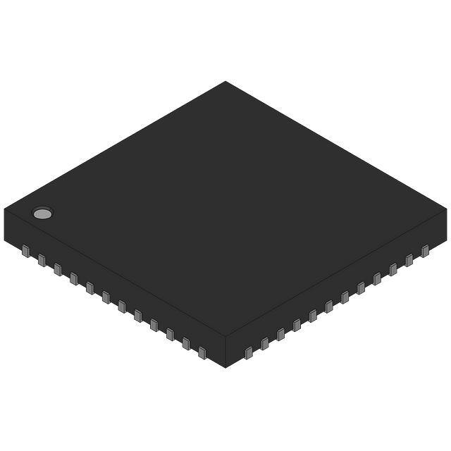


 工商网监
湘ICP备2023018690号
工商网监
湘ICP备2023018690号
