Product
Folder
Sample &
Buy
Technical
Documents
Support &
Community
Tools &
Software
SN74LV4052A-Q1
SCLS469F – MARCH 2003 – REVISED DECEMBER 2014
SN74LV4052A-Q1 Dual 4-Channel Analog Multiplexers and Demultiplexers
1 Features
3 Description
•
•
These dual 4-channel CMOS analog multiplexers and
demultiplexers are designed for 2-V to 5.5-V VCC
operation.
1
•
•
•
•
•
Qualified for Automotive Applications
AEC-Q100 Qualified With the Following Results:
– Device Temperature Grade 1: –40°C to
+125°C Ambient Operating Temperature
Range
– Device HBM ESD Classification Level 2
– Device CDM ESD Classification Level C4B
Supports Mixed-Mode Voltage Operation on All
Ports
Fast Switching
High On-Off Output-Voltage Ratio
Low Crosstalk Between Switches
Extremely Low Input Current
Applications include signal gating, chopping,
modulation or demodulation (modem), and signal
multiplexing for analog-to-digital and digital-to-analog
conversion systems.
Device Information(1)
PART NUMBER
SN74LV4052A-Q1
PACKAGE
BODY SIZE (NOM)
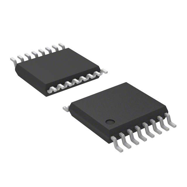
TSSOP (16)
5.00 mm × 4.40 mm
SOIC (16)
9.90 mm × 3.91 mm
(1) For all available packages, see the orderable addendum at
the end of the datasheet.
2 Applications
•
The SN7LV4052A-Q1 devices handle both analog
and digital signals. Each channel permits signals with
amplitudes up to 5.5 V (peak).
Automotive:
– Signal Gating
– Chopping
– Modulation or Demodulation (Modem)
– Signal Multiplexing for Analog-to-Digital and
Digital-to-Analog Conversion Systems
Logic Diagram (Positive Logic)
13
1-COM
12
10
14
15
9
11
1
5
2
4
6
3
1Y0
1Y1
1Y2
1Y3
2Y0
2Y1
2Y2
2Y3
2-COM
1
An IMPORTANT NOTICE at the end of this data sheet addresses availability, warranty, changes, use in safety-critical applications,
intellectual property matters and other important disclaimers. PRODUCTION DATA.
�SN74LV4052A-Q1
SCLS469F – MARCH 2003 – REVISED DECEMBER 2014
www.ti.com
Table of Contents
1
2
3
4
5
6
7
8
Features ..................................................................
Applications ...........................................................
Description .............................................................
Revision History.....................................................
Pin Configuration and Functions .........................
Specifications.........................................................
1
1
1
2
3
4
6.1
6.2
6.3
6.4
6.5
6.6
6.7
6.8
6.9
4
4
4
5
5
5
5
6
6
Absolute Maximum Ratings .....................................
ESD Ratings ............................................................
Recommended Operating Conditions ......................
Thermal Information ..................................................
Operating Characteristics..........................................
Electrical Characteristics...........................................
Switching Characteristics VCC = 3.3 V ± 0.3 V .........
Switching Characteristics VCC = 5 V ± 0.5 V ............
Analog Switch Characteristics ..................................
Parameter Measurement Information .................. 7
Detailed Description ............................................ 11
8.1
8.2
8.3
8.4
9
Overview .................................................................
Functional Block Diagram .......................................
Feature Description.................................................
Device Functional Modes........................................
11
11
11
11
Application and Implementation ........................ 12
9.1 Application Information............................................ 12
9.2 Typical Application ................................................. 12
10 Power Supply Recommendations ..................... 13
11 Layout................................................................... 13
11.1 Layout Guidelines ................................................. 13
11.2 Layout Example .................................................... 13
12 Device and Documentation Support ................. 14
12.1 Trademarks ........................................................... 14
12.2 Electrostatic Discharge Caution ............................ 14
12.3 Glossary ................................................................ 14
13 Mechanical, Packaging, and Orderable
Information ........................................................... 14
4 Revision History
NOTE: Page numbers for previous revisions may differ from page numbers in the current version.
Changes from Revision E (November 2012) to Revision F
•
Page
Added ESD Ratings table, Feature Description section, Device Functional Modes, Application and Implementation
section, Power Supply Recommendations section, Layout section, Device and Documentation Support section, and
Mechanical, Packaging, and Orderable Information section ................................................................................................. 4
Changes from Revision D (June 2011) to Revision E
Page
•
Deleted θJA row from Absolute Maximum Ratings table......................................................................................................... 4
•
Added Thermal Information table ........................................................................................................................................... 5
•
Corrected second row of Function Table ............................................................................................................................. 11
2
Submit Documentation Feedback
Copyright © 2003–2014, Texas Instruments Incorporated
Product Folder Links: SN74LV4052A-Q1
�SN74LV4052A-Q1
www.ti.com
SCLS469F – MARCH 2003 – REVISED DECEMBER 2014
5 Pin Configuration and Functions
D OR PW PACKAGE
(TOP VIEW)
2Y0
2Y2
2-COM
2Y3
2Y1
INH
GND
GND
VCC
1Y2
1Y1
1-COM
1Y0
1Y3
A
B
Pin Functions
PIN
NO.
(1)
NAME
I/O (1)
DESCRIPTION
1
2Y0
I (1)
Input to mux 2
2
2Y2
I (1)
Input to mux 2
(1)
3
2-COM
O
4
2Y3
I (1)
Output of mux 2
Input to mux 2
5
2Y1
I (1)
Input to mux 2
6
INH
I
Enables the outputs of the device. Logic low level with turn the outputs on, high level will turn
them off.
7
GND
-
Ground
8
GND
-
Ground
9
B
I
Selector line for outputs (see Device Functional Modes for specific information)
10
A
I
Selector line for outputs (see Device Functional Modes for specific information)
11
1Y3
I (1)
Input to mux 1
12
1Y0
I (1)
Input to mux 1
(1)
13
1-COM
O
14
1Y1
I (1)
Output of mux 1
Input to mux 1
15
1Y2
I (1)
Input to mux 1
16
Vcc
I
Device power input
These I/O descriptions represent the device when used as a multiplexer, when this device is operated as a demultiplexer pins 1Y0, 1Y1,
1Y2, 1Y3, 2Y0, 2Y1, 2Y2, 2Y3 may be considered outputs (O) and pins 1-COM and 2-COM may be considered inputs (I).
Submit Documentation Feedback
Copyright © 2003–2014, Texas Instruments Incorporated
Product Folder Links: SN74LV4052A-Q1
3
�SN74LV4052A-Q1
SCLS469F – MARCH 2003 – REVISED DECEMBER 2014
www.ti.com
6 Specifications
6.1 Absolute Maximum Ratings (1)
over operating free-air temperature range (unless otherwise noted)
VCC Supply voltage range
VI
Input voltage range (2)
VIO
Switch I/O voltage range (2)
IIK
Input clamp current
(3)
MIN
MAX
–0.5
7
–0.5
7
–0.5
VCC + 0.5
VI < 0
–20
IIOK I/O diode current
VIO < 0
–50
IT
VIO = 0 to VCC
Switch through current
mA
±50
Tstg Storage temperature range
(2)
(3)
V
±25
Continuous current through VCC or GND
(1)
UNIT
–65
150
°C
Stresses beyond those listed under Absolute Maximum Ratings may cause permanent damage to the device. These are stress ratings
only, and functional operation of the device at these or any other conditions beyond those indicated under Recommended Operating
Conditions is not implied. Exposure to absolute-maximum-rated conditions for extended periods may affect device reliability.
The input and output negative-voltage ratings may be exceeded if the input and output current ratings are observed.
The maximum limit for this value is 5.5 V.
6.2 ESD Ratings
VALUE
Human body model (HBM), per AEC Q100-002 (1)
V(ESD)
(1)
Electrostatic discharge
Charged device model (CDM), per
AEC Q100-011
UNIT
±2000
Corner pins (2Y0, GND, VCC,
and B)
±750
Other pins
±500
V
AEC Q100-002 indicates HBM stressing is done in accordance with the ANSI/ESDA/JEDEC JS-001 specification.
6.3 Recommended Operating Conditions (1)
MIN
VCC
2 (2)
Supply voltage
VCC = 2 V
High-level input voltage,
control inputs
VIH
NOM
MAX
5.5
UNIT
V
1.5
VCC = 2.3 V to 2.7 V
VCC × 0.7
VCC = 3 V to 3.6 V
VCC × 0.7
VCC = 4.5 V to 5.5 V
VCC × 0.7
VCC = 2 V
V
0.5
VCC = 2.3 V to 2.7 V
VCC × 0.3
VCC = 3 V to 3.6 V
VCC × 0.3
VIL
Low-level input voltage,
control inputs
VI
Control input voltage
0
5.5
V
VIO
Input/output voltage
0
VCC
V
Δt/Δ
v
Input transition rise or fall rate
VCC = 4.5 V to 5.5 V
VCC × 0.3
VCC = 2.3 V to 2.7 V
200
VCC = 3 V to 3.6 V
100
VCC = 4.5 V to 5.5 V
Operating free-air temperature
SN74LV4052ATDRQ1,
SN74LV4052ATPWRQ1
–40
105
TA
Operating free-air temperature
SN74LV4052AQPWRQ1
–40
125
(2)
4
ns/V
20
TA
(1)
V
°C
Hold all unused inputs of the device at VCC or GND to ensure proper device operation. See the TI application report, Implications of
Slow or Floating CMOS Inputs, literature number SCBA004.
With supply voltages at or near 2 V, the analog switch on-state resistance becomes very nonlinear. TI recommends transmitting only
digital signals at these low supply voltages.
Submit Documentation Feedback
Copyright © 2003–2014, Texas Instruments Incorporated
Product Folder Links: SN74LV4052A-Q1
�SN74LV4052A-Q1
www.ti.com
SCLS469F – MARCH 2003 – REVISED DECEMBER 2014
6.4 Thermal Information
SN74LV4052A-Q1
THERMAL METRIC
D
PW
16 PINS
16 PINS
UNIT
RθJA
Junction-to-ambient thermal resistance
85.9
113.3
°C/W
RθJC(top)
Junction-to-case (top) thermal resistance
44.6
48.1
°C/W
RθJB
Junction-to-board thermal resistance
43.4
58.4
°C/W
ψJT
Junction-to-top characterization parameter
13.4
6.2
°C/W
ψJB
Junction-to-board characterization parameter
43.1
57.8
°C/W
6.5 Operating Characteristics
VCC = 3.3 V, TA = 25°C (unless otherwise noted)
PARAMETER
Cpd
TEST CONDITIONS
Power dissipation capacitance
CL = 50 pF, f = 10 MHz
TYP
UNIT
11.8
pF
6.6 Electrical Characteristics
over recommended operating free-air temperature range (unless otherwise noted)
PARAMETER
TEST CONDITIONS
IT = 2 mA,
VI = VCC or GND,
VINH = VIL
(see Figure 1)
On-state switch
resistance
ron
ron(
IT = 2 mA,
VI = VCC or GND,
VINH = VIL
Peak on-state
resistance
p)
VCC
TA = -40 to 105°C
MIN
TA = -40 to 125°C
TYP
MAX
MIN
TYP
MAX
2.3 V
225
225
3V
190
190
4.5 V
100
100
2.3 V
600
600
3V
225
225
4.5 V
125
125
2.3 V
40
40
3V
30
30
4.5 V
20
20
UNIT
Ω
Ω
Difference in on-state
resistance between
switch
IT = 2 mA,
VI = VCC or GND,
VINH = VIL
Control input current
VI = 5.5 V or GND
0 V to
5.5 V
±1
±2
μA
IS(of Off-state switch
leakage current
f)
VI = VCC and
VO = GND, or
VI = GND and
VO = VCC,
VINH = VIH
(see Figure 2)
5.5 V
±1
±2
μA
IS(o
Δro
n
II
Ω
On-state switch
leakage current
VI = VCC or GND,
VINH = VIL
(see Figure 3)
5.5 V
±1
±2
μA
n)
ICC
Supply current
VI = VCC or GND
5.5 V
20
40
μA
6.7 Switching Characteristics VCC = 3.3 V ± 0.3 V
over recommended operating free-air temperature range (unless otherwise noted)
tPLH
tPHL
tPZH
tPZL
tPHZ
tPLZ
TA = -40 to 105°C
TA = -40 to 125°C
FROM
(INPUT)
TO
(OUTPUT
TEST
CONDITIONS
Propagation
delay time
COM or Y
Y or COM
CL = 50 pF
(see Figure 4)
12
14
ns
Enable delay
time
INH
COM or Y
CL = 50 pF
(see Figure 5)
25
25
ns
Disable delay
time
INH
COM or Y
CL = 50 pF
(see Figure 5)
25
25
ns
PARAMETER
MIN
TYP
MAX
MIN
TYP
MAX
Submit Documentation Feedback
Copyright © 2003–2014, Texas Instruments Incorporated
Product Folder Links: SN74LV4052A-Q1
UNIT
5
�SN74LV4052A-Q1
SCLS469F – MARCH 2003 – REVISED DECEMBER 2014
www.ti.com
6.8 Switching Characteristics VCC = 5 V ± 0.5 V
over recommended operating free-air temperature range (unless otherwise noted)
tPLH
tPHL
tPZH
tPZL
tPHZ
tPLZ
TA = -40 to 105°C
TA = -40 to 125°C
FROM
(INPUT)
TO
(OUTPUT
TEST
CONDITIONS
Propagation
delay time
COM or Y
Y or COM
CL = 50 pF
(see Figure 4)
8
10
ns
Enable delay
time
INH
COM or Y
CL = 50 pF
(see Figure 5)
18
18
ns
Disable delay
time
INH
COM or Y
CL = 50 pF
(see Figure 5)
18
18
ns
PARAMETER
MIN
TYP
MAX
MIN
TYP
MAX
UNIT
6.9 Analog Switch Characteristics
over recommended operating free-air temperature range (unless otherwise noted)
PARAMETER
Frequency response
(switch on)
Crosstalk
(between any
switches))
Crosstalk
(control input to signal
output)
Feedthrough
attenuation
(switch off)
Sine-wave distortion
(1)
(2)
6
TA = 25°C
FROM
(INPUT)
TO
(OUTPUT)
30
Y or COM
CL = 50 pF,
RL = 600 Ω,
fin = 1 MHz (sine wave) (1)
(see Figure 6)
2.3 V
COM or Y
3V
35
4.5 V
50
2.3 V
–45
Y or COM
CL = 50 pF,
RL = 600 Ω,
fin = 1 MHz (sine wave)
(seeFigure 7 )
3V
–45
4.5 V
–45
2.3 V
20
COM or Y
CL = 50 pF,
RL = 600 Ω,
fin = 1 MHz (square wave)
(see Figure 8)
3V
35
4.5 V
65
2.3 V
–45
Y or COM
CL = 50 pF,
RL = 600 Ω,
fin = 1 MHz (2)
(see Figure 9)
3V
–45
Y or COM
CL = 50 pF,
RL = 10 kΩ,
fin = 1 kHz (sine
wave)
(see Figure 10)
COM or Y
INH
COM or Y
COM or Y
TEST CONDITIONS
VCC
VI = 2 Vp-p
VI = 2.5 Vp-p
VI = 4 Vp-p
MIN
TYP
4.5 V
–45
2.3 V
0.1%
3V
0.1%
4.5 V
0.1%
MAX
UNIT
MHz
dB
mV
dB
Adjust fin voltage to obtain 0-dBm output. Increase fin frequency until dB meter reads −3 dB.
Adjust fin voltage to obtain 0-dBm input.
Submit Documentation Feedback
Copyright © 2003–2014, Texas Instruments Incorporated
Product Folder Links: SN74LV4052A-Q1
�SN74LV4052A-Q1
www.ti.com
SCLS469F – MARCH 2003 – REVISED DECEMBER 2014
7 Parameter Measurement Information
=
x
W
–
Figure 1. On-State Resistance Test Circuit
Figure 2. Off-State Switch Leakage-Current Test Circuit
Figure 3. On-State Switch Leakage-Current Test Circuit
W
Figure 4. Propagation Delay Time, Signal Input to Signal Output
Submit Documentation Feedback
Copyright © 2003–2014, Texas Instruments Incorporated
Product Folder Links: SN74LV4052A-Q1
7
�SN74LV4052A-Q1
SCLS469F – MARCH 2003 – REVISED DECEMBER 2014
www.ti.com
Parameter Measurement Information (continued)
W
W
≈
≈
≈
–
≈
Figure 5. Switching Time (tPZL, tPLZ, tPZH, tPHZ), Control to Signal Output
m
W
= 50 pF
= 600 W
Figure 6. Frequency Response (Switch On)
8
Submit Documentation Feedback
Copyright © 2003–2014, Texas Instruments Incorporated
Product Folder Links: SN74LV4052A-Q1
�SN74LV4052A-Q1
www.ti.com
SCLS469F – MARCH 2003 – REVISED DECEMBER 2014
Parameter Measurement Information (continued)
m
600 W
W
= 50 pF
= 600 W
(OFF)
= 50 pF
= 600 W
600 W
Figure 7. Crosstalk Between Any Two Switches
W
W
= 50 pF
= 600 W
Figure 8. Crosstalk Between Control Input and Switch Output
10 m
W
= 50 pF
= 10 kW
Figure 9. Feedthrough Attenuation (Switch Off)
Submit Documentation Feedback
Copyright © 2003–2014, Texas Instruments Incorporated
Product Folder Links: SN74LV4052A-Q1
9
�SN74LV4052A-Q1
SCLS469F – MARCH 2003 – REVISED DECEMBER 2014
www.ti.com
Parameter Measurement Information (continued)
10 m
W
= 10 kW
= 50 pF
Figure 10. Sine-Wave Distortion
10
Submit Documentation Feedback
Copyright © 2003–2014, Texas Instruments Incorporated
Product Folder Links: SN74LV4052A-Q1
�SN74LV4052A-Q1
www.ti.com
SCLS469F – MARCH 2003 – REVISED DECEMBER 2014
8 Detailed Description
8.1 Overview
This device is a dual 4-channel analog multiplexer. A multiplexer is often used when several signals need to
share the same device or resource. This device allows the selection of one of these signals at a time for analysis
or propagation.
8.2 Functional Block Diagram
13
1-COM
12
10
14
15
9
11
1
5
2
4
6
3
1Y0
1Y1
1Y2
1Y3
2Y0
2Y1
2Y2
2Y3
2-COM
8.3 Feature Description
This device contains 2 separate 4-channel multiplexers for use in a variety of applications. The 4-channel
multiplexers can also be configured as demultiplexers by using the COM pins as inputs and the 1Yx or 2Yx pins
as outputs. This device is qualified for automotive applications and has an extended temperature range of -40C
to 125C (maximum depends on package type).
8.4 Device Functional Modes
Table 1. Function Table
INPUTS
INH
B
A
ON
CHANNEL
L
L
L
1Y0, 2Y0
L
L
H
1Y1, 2Y1
L
H
L
1Y2, 2Y2
L
H
H
1Y3, 2Y3
H
X
X
None
Submit Documentation Feedback
Copyright © 2003–2014, Texas Instruments Incorporated
Product Folder Links: SN74LV4052A-Q1
11
�SN74LV4052A-Q1
SCLS469F – MARCH 2003 – REVISED DECEMBER 2014
www.ti.com
9 Application and Implementation
NOTE
Information in the following applications sections is not part of the TI component
specification, and TI does not warrant its accuracy or completeness. TI’s customers are
responsible for determining suitability of components for their purposes. Customers should
validate and test their design implementation to confirm system functionality.
9.1 Application Information
A multiplexer is used in applications where multiple signals share a resource. In the example below, several
different sensors are connected to the analog-to-digital converter (ADC) of a microcontroller (MCU).
9.2 Typical Application
Figure 11. Typical Application Schematic
9.2.1 Design Requirements
Normally processing 8 different analog signals would require 8 separate ADCs, but this figure shows how to
achieve this using only 2 ADCs and 3 GPIOs (general purpose input/outputs).
9.2.2 Detailed Design Procedure
To design with the SN74LV4052A-Q1, a stable input voltage between 2V (see Recommended Operating
Conditions (1) for details) and 5.5 V must be available. Another important design consideration would be the
characteristics of the signal that is being multiplexed to make sure no important information is lost due to timing
or voltage level incompatibility with this device.
(1)
12
Hold all unused inputs of the device at VCC or GND to ensure proper device operation. See the TI application report, Implications of
Slow or Floating CMOS Inputs, literature number SCBA004.
Submit Documentation Feedback
Copyright © 2003–2014, Texas Instruments Incorporated
Product Folder Links: SN74LV4052A-Q1
�SN74LV4052A-Q1
www.ti.com
SCLS469F – MARCH 2003 – REVISED DECEMBER 2014
10 Power Supply Recommendations
Most systems have a common 3.3 V or 5 V rail that may be used to supply the VCC pin of this device. If this is
not available, a Switch-Mode-Power-Supply (SMPS) or a Linear Dropout Regulator (LDO) may be used to supply
this device from a higher voltage rail.
11 Layout
11.1 Layout Guidelines
In general, it is best to keep signal lines as short and as straight as possible. Incorporation of microstrip or
stripline techniques is also recommended when signal lines are greater than 1 inch in length. These traces must
be designed with a characteristic impedance of either 50 Ω or 75 Ω,as required by the application. Be careful
placing this device too close to high voltage switching components, as they may cause interference.
11.2 Layout Example
Figure 12. Layout Example Schematic
Submit Documentation Feedback
Copyright © 2003–2014, Texas Instruments Incorporated
Product Folder Links: SN74LV4052A-Q1
13
�SN74LV4052A-Q1
SCLS469F – MARCH 2003 – REVISED DECEMBER 2014
www.ti.com
12 Device and Documentation Support
12.1 Trademarks
All trademarks are the property of their respective owners.
12.2 Electrostatic Discharge Caution
These devices have limited built-in ESD protection. The leads should be shorted together or the device placed in conductive foam
during storage or handling to prevent electrostatic damage to the MOS gates.
12.3 Glossary
SLYZ022 — TI Glossary.
This glossary lists and explains terms, acronyms, and definitions.
13 Mechanical, Packaging, and Orderable Information
The following pages include mechanical, packaging, and orderable information. This information is the most
current data available for the designated devices. This data is subject to change without notice and revision of
this document. For browser-based versions of this data sheet, refer to the left-hand navigation.
14
Submit Documentation Feedback
Copyright © 2003–2014, Texas Instruments Incorporated
Product Folder Links: SN74LV4052A-Q1
�PACKAGE OPTION ADDENDUM
www.ti.com
10-Dec-2020
PACKAGING INFORMATION
Orderable Device
Status
(1)
Package Type Package Pins Package
Drawing
Qty
Eco Plan
(2)
Lead finish/
Ball material
MSL Peak Temp
Op Temp (°C)
Device Marking
(3)
(4/5)
(6)
CLV4052ATPWRG4Q1
ACTIVE
TSSOP
PW
16
2000
RoHS & Green
NIPDAU
Level-1-260C-UNLIM
-40 to 105
L4052AQ
SN74LV4052AQPWRQ1
ACTIVE
TSSOP
PW
16
2000
RoHS & Green
NIPDAU
Level-1-260C-UNLIM
-40 to 125
4052AQ1
SN74LV4052ATDRQ1
ACTIVE
SOIC
D
16
2500
RoHS & Green
NIPDAU
Level-1-260C-UNLIM
-40 to 105
L4052AQ
SN74LV4052ATPWRQ1
ACTIVE
TSSOP
PW
16
2000
RoHS & Green
NIPDAU
Level-1-260C-UNLIM
-40 to 105
L4052AQ
(1)
The marketing status values are defined as follows:
ACTIVE: Product device recommended for new designs.
LIFEBUY: TI has announced that the device will be discontinued, and a lifetime-buy period is in effect.
NRND: Not recommended for new designs. Device is in production to support existing customers, but TI does not recommend using this part in a new design.
PREVIEW: Device has been announced but is not in production. Samples may or may not be available.
OBSOLETE: TI has discontinued the production of the device.
(2)
RoHS: TI defines "RoHS" to mean semiconductor products that are compliant with the current EU RoHS requirements for all 10 RoHS substances, including the requirement that RoHS substance
do not exceed 0.1% by weight in homogeneous materials. Where designed to be soldered at high temperatures, "RoHS" products are suitable for use in specified lead-free processes. TI may
reference these types of products as "Pb-Free".
RoHS Exempt: TI defines "RoHS Exempt" to mean products that contain lead but are compliant with EU RoHS pursuant to a specific EU RoHS exemption.
Green: TI defines "Green" to mean the content of Chlorine (Cl) and Bromine (Br) based flame retardants meet JS709B low halogen requirements of


 工商网监
湘ICP备2023018690号
工商网监
湘ICP备2023018690号
