Product
Folder
Sample &
Buy
Technical
Documents
Support &
Community
Tools &
Software
SN74VMEH22501A-EP
SCES625A – FEBRUARY 2005 – REVISED NOVEMBER 2015
SN74VMEH22501A-EP 8-Bit Universal Bus Transceiver and Two 1-Bit Bus Transceivers
With Split LVTTL Port, Feedback Path, and 3-State Outputs
1 Features
2 Applications
•
•
•
•
1
•
•
•
•
•
•
•
•
•
•
•
•
•
•
•
•
•
•
Controlled Baseline
– One Assembly/Test Site, One Fabrication Site
Enhanced Diminishing Manufacturing Sources
(DMS) Support
Enhanced Product-Change Notification
Qualification Pedigree(1)
Member of the Texas Instruments Widebus™
Family
UBT™ Transceiver Combines D-Type Latches
and D-Type Flip-Flops for Operation in
Transparent, Latched, or Clocked Modes
OEC™ Circuitry Improves Signal Integrity and
Reduces Electromagnetic Interference (EMI)
Compliant With VME64, 2eVME, and 2eSST
Protocols Validated at TA = –40°C to 85°C
Bus Transceiver Split LVTTL Port Provides a
Feedback Path for Control and Diagnostics
Monitoring
I/O Interfaces are 5-V Tolerant
B-Port Outputs (–48 mA/64 mA)
Y and A-Port Outputs (–12 mA/12 mA)
Ioff, Power-Up 3-State, and BIAS VCC Support Live
Insertion
Bus Hold on 3A-Port Data Inputs
26-Ω Equivalent Series Resistor on 3A Ports and
Y Outputs
Flow-Through Architecture Facilitates Printed
Circuit Board Layout
Distributed VCC and GND Pins Minimize HighSpeed Switching Noise
Latch-Up Performance Exceeds 100 mA Per
JESD 78, Class II
ESD Protection Exceeds JESD 22
– 2000-V Human-Body Model (A114-A)
– 200-V Machine Model (A115-A)
– 1000-V Charged-Device Model (C101)
Industrial Controls
Telecommunications
Instrumentation Systems
3 Description
The SN74VMEH22501A-EP 8-bit universal bus
transceiver has two integral 1-bit three-wire bus
transceivers and is designed for 3.3-V VCC operation
with 5-V tolerant inputs. The UBT transceiver allows
transparent, latched, and flip-flop modes of data
transfer, and the separate LVTTL input and outputs
on the bus transceivers provide a feedback path for
control and diagnostics monitoring. This device
provides a high-speed interface between cards
operating at LVTTL logic levels and VME64, VME64x,
or VME320(2) backplane topologies.
Device Information(3)
PART NUMBER
SN74VMEH22501A-EP
PACKAGE
BODY SIZE (NOM)
TSSOP (48)
4.40 mm × 9.70 mm
TVSOP (48)
6.10 mm × 12.50 mm
(1) Component qualification in accordance with JEDEC and
industry standards to ensure reliable operation over an
extended temperature range. This includes, but is not limited
to, Highly Accelerated Stress Test (HAST) or biased 85/85,
temperature
cycle,
autoclave
or
unbiased
HAST,
electromigration, bond intermetallic life, and mold compound
life. Such qualification testing should not be viewed as
justifying use of this component beyond specified
performance and environmental limits.
(2) VME320 is a patented backplane construction by Arizona
Digital, Inc.
(3) For all available packages, see the orderable addendum at
the end of the data sheet.
Logic Diagram (Positive Logic)
1OEAB 48
1OEBY 1
1A 2
46 1B
1Y 3
2OEAB 41
2OEBY 8
43
2A 5
2B
2Y 6
OE 14
DIR 24
CLKAB 32
LE 11
CLKBA 17
3A1 9
1D
C1
CLK
1D
C1
CLK
40 3B1
To Seven Other Channels
Pin numbers shown for DGG and DGV
1
An IMPORTANT NOTICE at the end of this data sheet addresses availability, warranty, changes, use in safety-critical applications,
intellectual property matters and other important disclaimers. PRODUCTION DATA.
�SN74VMEH22501A-EP
SCES625A – FEBRUARY 2005 – REVISED NOVEMBER 2015
www.ti.com
Table of Contents
1
2
3
4
5
6
7
Features ..................................................................
Applications ...........................................................
Description .............................................................
Revision History.....................................................
Description (continued).........................................
Pin Configuration and Functions .........................
Specifications.........................................................
7.1
7.2
7.3
7.4
7.5
7.6
7.7
7.19 Skew Characteristics for UBT (M Version) ...........
7.20 Skew Characteristics for Bus Transceiver (I
Version)....................................................................
7.21 Skew Characteristics for UBT (I Version) .............
7.22 Skew Characteristics for Bus Transceiver (I
Version)....................................................................
7.23 Skew Characteristics for UBT (I Version) .............
7.24 Maximum Data Transfer Rates .............................
7.25 Typical Characteristics ..........................................
1
1
1
2
3
4
6
Absolute Maximum Ratings ...................................... 6
ESD Ratings.............................................................. 6
Recommended Operating Conditions....................... 7
Thermal Information .................................................. 7
Electrical Characteristics........................................... 8
Live-Insertion Specifications ..................................... 9
Timing Requirements for UBT Transceiver (I
Version)...................................................................... 9
7.8 Switching Characteristics for Bus Transceiver
Function (I Version).................................................. 10
7.9 Switching Characteristics for Bus Transceiver
Function (M Version)................................................ 10
7.10 Switching Characteristics for UBT Transceiver (I
Version).................................................................... 11
7.11 Switching Characteristics for UBT Transceiver (M
Version).................................................................... 12
7.12 Switching Characteristics for Bus Transceiver
Function (I Version).................................................. 12
7.13 Switching Characteristics for UBT (I Version)....... 13
7.14 Switching Characteristics for Bus Transceiver
Function (I Version).................................................. 13
7.15 Switching Characteristics for UBT (I Version)....... 13
7.16 Skew Characteristics for Bus Transceiver (I
Version).................................................................... 14
7.17 Skew Characteristics for Bus Transceiver (M
Version).................................................................... 15
7.18 Skew Characteristics for UBT (I Version) ............. 15
8
15
17
17
17
18
18
19
Parameter Measurement Information ................ 20
8.1 Distributed-Load Backplane Switching
Characteristics ......................................................... 20
9
Detailed Description ............................................ 23
9.1
9.2
9.3
9.4
Overview .................................................................
Functional Block Diagram .......................................
Feature Description.................................................
Device Functional Modes........................................
23
24
25
27
10 Application and Implementation........................ 28
10.1 Application Information.......................................... 28
10.2 Typical Application ............................................... 28
11 Power Supply Recommendations ..................... 30
12 Layout................................................................... 30
12.1 Layout Guidelines ................................................. 30
12.2 Layout Example .................................................... 31
13 Device and Documentation Support ................. 32
13.1
13.2
13.3
13.4
13.5
13.6
Device Support......................................................
Related Links ........................................................
Community Resources..........................................
Trademarks ...........................................................
Electrostatic Discharge Caution ............................
Glossary ................................................................
32
32
32
32
32
32
14 Mechanical, Packaging, and Orderable
Information ........................................................... 32
4 Revision History
NOTE: Page numbers for previous revisions may differ from page numbers in the current version.
Changes from Original (February 2005) to Revision A
Page
•
Added ESD Ratings table, Feature Description section, Device Functional Modes, Application and Implementation
section, Power Supply Recommendations section, Layout section, Device and Documentation Support section, and
Mechanical, Packaging, and Orderable Information section ................................................................................................. 1
•
Removed Ordering Information table. ................................................................................................................................... 1
•
Added junction temperature and removed package thermal impedance from Absolute Maximum Ratings ......................... 6
•
Added different conditions and results for I and M versions to the Specifications ................................................................ 7
•
Updated the VCC test condition for IOZ(PU/PD) .......................................................................................................................... 8
•
Added Community Resources ............................................................................................................................................. 32
2
Submit Documentation Feedback
Copyright © 2005–2015, Texas Instruments Incorporated
Product Folder Links: SN74VMEH22501A-EP
�SN74VMEH22501A-EP
www.ti.com
SCES625A – FEBRUARY 2005 – REVISED NOVEMBER 2015
5 Description (continued)
The SN74VMEH22501A-EP device is pin-for-pin compatible to the SN74VMEH22501 device (SCES357), but
operates at a wider operating temperature range.
High-speed backplane operation is a direct result of the improved OEC circuitry and high drive that has been
designed and tested into the VME64x backplane model. The B-port I/Os are optimized for driving large capacitive
loads and include pseudo-ETL input thresholds (½ VCC ±50 mV) for increased noise immunity. These
specifications support the 2eVME protocols in VME64x (ANSI/VITA 1.1) and 2eSST protocols in VITA 1.5.
With proper design of a 21-slot VME system, a designer can achieve 320-MB transfer rates on linear backplanes
and, possibly, 1-GB transfer rates on the VME320 backplane.
All inputs and outputs are 5-V tolerant and are compatible with TTL and 5-V CMOS inputs.
Active bus-hold circuitry holds unused or undriven 3A-port inputs at a valid logic state. Bus-hold circuitry is not
provided on 1A or 2A inputs, any B-port input, or any control input. Use of pullup or pulldown resistors with the
bus-hold circuitry is not recommended.
This device is fully specified for live-insertion applications using Ioff, power-up 3-state, and BIAS VCC. The Ioff
circuitry prevents damaging current to backflow through the device when it is powered off/on. The power-up 3state circuitry places the outputs in the high-impedance state during power up and power down, which prevents
driver conflict. The BIAS VCC circuitry precharges and preconditions the B-port input/output connections,
preventing disturbance of active data on the backplane during card insertion or removal, and permits true liveinsertion capability.
When VCC is between 0 and 1.5 V, the device is in the high-impedance state during power up or power down.
However, to ensure the high-impedance state above 1.5 V, output-enable (OE and OEBY) inputs should be tied
to VCC through a pullup resistor and output-enable (OEAB) inputs should be tied to GND through a pulldown
resistor; the minimum value of the resistor is determined by the drive capability of the device connected to this
input.
Copyright © 2005–2015, Texas Instruments Incorporated
Product Folder Links: SN74VMEH22501A-EP
Submit Documentation Feedback
3
�SN74VMEH22501A-EP
SCES625A – FEBRUARY 2005 – REVISED NOVEMBER 2015
www.ti.com
6 Pin Configuration and Functions
DGG or DGV Package
48-Pin TSSOP or TVSOP
Top View
Pin Functions
PIN
NAME
NO.
I/O
DESCRIPTION
1OEBY
1
I
Active low control output for 1Y bus
1A
2
I
Data in to 1B
1Y
3
O
Data out
GND
4
—
Ground
2A
5
I
Data in to 2B
2Y
6
O
Data out
VCC
7
I
Power supply input for internal circuits
2OEBY
8
I
Active low control output for 2Y bus
3A1
9
I/O
Data in/out
GND
10
—
Ground
LE
11
I
3A2
12
I/O
4
Submit Documentation Feedback
Latch Enable pin for UBT
Data in/out
Copyright © 2005–2015, Texas Instruments Incorporated
Product Folder Links: SN74VMEH22501A-EP
�SN74VMEH22501A-EP
www.ti.com
SCES625A – FEBRUARY 2005 – REVISED NOVEMBER 2015
Pin Functions (continued)
PIN
NAME
NO.
I/O
DESCRIPTION
3A3
13
I/O
OE
14
I
Data in/out
GND
15
—
Ground
3A4
16
I/O
Data in/out
CLKBA
17
I
Clock for 3B data to 3A bus
VCC
18
I
Power supply input for internal circuits
3A5
19
I/O
Data in/out
3A6
20
I/O
Data in/out
GND
21
—
Ground
3A6
22
I/O
Data in/out
3A8
23
I/O
Data in/out
DIR
24
—
Direction control for UBT
VCC
25
I
3B8
26
I/O
Data in/out
3B7
27
I/O
Data in/out
GND
28
—
Ground
3B6
29
I/O
Data in/out
3B5
30
I/O
Data in/out
VCC
31
I
Power supply input for internal circuits
CLKAB
32
I
Clock for 3A data to 3B bus
3B4
33
I/O
Data in/out
GND
34
—
Ground
VCC
35
I
3B3
36
I/O
Data in/out
3B2
37
I/O
Data in/out
VCC
38
I
GND
39
—
Ground
3B1
40
I/O
Data in/out
2OEAB
41
I
Active high control output for 2B bus
VCC
42
I
Power supply input for internal circuits
2B
43
I/O
BIAS VCC
44
I
GND
45
—
Ground
1B
46
I/O
Data in/out
VCC
47
I
Power supply input for internal circuits
1OEAB
48
I
Active high control output for 1B bus
Active low enable pin for UBT
Power supply input for internal circuits
Power supply input for internal circuits
Power supply input for internal circuits
Data in/out
Power supply input for internal circuits
Copyright © 2005–2015, Texas Instruments Incorporated
Product Folder Links: SN74VMEH22501A-EP
Submit Documentation Feedback
5
�SN74VMEH22501A-EP
SCES625A – FEBRUARY 2005 – REVISED NOVEMBER 2015
www.ti.com
7 Specifications
7.1 Absolute Maximum Ratings
over operating free-air temperature range (unless otherwise noted)
VCC,
BIAS VCC
(1)
MIN
MAX
UNIT
Supply voltage
–0.5
4.6
V
(2)
–0.5
7
V
–0.5
7
V
3A port or Y output
–0.5
VCC + 0.5
B port
–0.5
4.6
VI
Input voltage
VO
Voltage applied to any output in the high-impedance or power-off state (2)
VO
Voltage applied to any output in the high or low state (2)
IO
Output current in the low state
IO
Output current in the high state
IIK
3A port or Y output
50
B port
100
V
mA
3A port or Y output
–50
B port
–100
Input clamp current
VI < 0
–50
mA
IOK
Output clamp current
VO < 0 or VO > VCC, B port
–50
mA
TJ
Junction temperature
–55
150
°C
Tstg
Storage temperature
–65
150
°C
(1)
(2)
mA
Stresses beyond those listed under Absolute Maximum Ratings may cause permanent damage to the device. These are stress ratings
only, and functional operation of the device at these or any other conditions beyond those indicated under Recommended Operating
Conditions is not implied. Exposure to absolute-maximum-rated conditions for extended periods may affect device reliability.
The input and output negative-voltage ratings may be exceeded if the input and output clamp-current ratings are observed.
7.2 ESD Ratings
VALUE
V(ESD)
(1)
(2)
6
Electrostatic discharge
Human-body model (HBM), per ANSI/ESDA/JEDEC JS-001
(1)
Charged-device model (CDM), per JEDEC specification JESD22-C101 (2)
±2000
±500
UNIT
V
JEDEC document JEP155 states that 500-V HBM allows safe manufacturing with a standard ESD control process.
JEDEC document JEP157 states that 250-V CDM allows safe manufacturing with a standard ESD control process.
Submit Documentation Feedback
Copyright © 2005–2015, Texas Instruments Incorporated
Product Folder Links: SN74VMEH22501A-EP
�SN74VMEH22501A-EP
www.ti.com
SCES625A – FEBRUARY 2005 – REVISED NOVEMBER 2015
7.3 Recommended Operating Conditions
see
(1) (2)
VCC,
BIAS VCC
Supply voltage
VI
Input voltage
VIH
MIN
NOM
MAX
UNIT
3.15
3.3
3.45
V
Control inputs or A
port
VCC
5.5
B port
VCC
5.5
Control inputs or A
port
High-level input voltage
B port
VIL
2
V
0.5 VCC + 50 mV
Control inputs or A
port
Low-level input voltage
0.8
B port
IIK
High-level output current
IOL
Low-level output current
Δt/Δv
Input transition rise or fall rate
Δt/ΔVCC
Power-up ramp rate
TA
Operating ambient temperature
(1)
(2)
V
0.5 VCC – 50 mV
Input clamp current
IOH
V
–18
3A port and Y output
–12
B port
–48
3A port and Y output
12
B port
64
Outputs enabled
mA
mA
mA
10
ns/V
20
µs/V
I version
–40
85
°C
M version
–55
125
°C
All unused control inputs of the device must be held at VCC or GND to ensure proper device operation. Refer to the TI application report,
Implications of Slow or Floating CMOS Inputs, SCBA004.
Proper connection sequence for use of the B-port I/O precharge feature is GND and BIAS VCC = 3.3 V first, I/O second, and VCC = 3.3 V
last, because the BIAS VCC precharge circuitry is disabled when any VCC pin is connected. The control inputs can be connected at any
time, but normally are connected during the I/O stage. If B-port precharge is not required, any connection sequence is acceptable, but
generally, GND is connected first.
7.4 Thermal Information
SN74VMEH22501A-EP
THERMAL METRIC
(1)
DGV (TVSOP)
DGG (TSSOP)
48 PINS
48 PINS
UNIT
RθJA
Junction-to-ambient thermal resistance, JEDEC 4-layer high-K board
73.9
62.9
°C/W
RθJC(top)
Junction-to-case (top) thermal resistance
26.1
15.8
°C/W
RθJB
Junction-to-board thermal resistance
37.3
30.0
°C/W
ψJT
Junction-to-top characterization parameter
1.9
0.7
°C/W
ψJB
Junction-to-board characterization parameter
36.8
29.7
°C/W
RθJC(bot)
Junction-to-case (bottom) thermal resistance
N/A
N/A
°C/W
(1)
For more information about traditional and new thermal metrics, see the Semiconductor and IC Package Thermal Metrics application
report, SPRA953.
Copyright © 2005–2015, Texas Instruments Incorporated
Product Folder Links: SN74VMEH22501A-EP
Submit Documentation Feedback
7
�SN74VMEH22501A-EP
SCES625A – FEBRUARY 2005 – REVISED NOVEMBER 2015
www.ti.com
7.5 Electrical Characteristics
over recommended operating free-air temperature range for A and B ports (unless otherwise noted)
PARAMETER
VIK
VOH
MIN TYP (1)
TEST CONDITIONS
VCC = 3.15 V
II = –18 mA
3A port, any B ports,
and Y outputs
VCC = 3.15 V to 3.45 V
IOH = –100 µA
3A port and Y outputs
VCC = 3.15 V
Any B port
VCC = 3.15 V
3A port, any B ports,
and Y outputs
VCC = 3.15 V to 3.45 V
VCC = 3.15 V
VOL
Any B port
–1.2
V
IOH = –6 mA
2.4
IOH = –12 mA
2
IOH = –24 mA
2.4
IOH = –48 mA
2
IOL = 100 µA
V
0.2
0.55
IOL = 12 mA; I version;
TA = –40 to 85°C
0.8
IOL = 12 mA; M version;
TA = –55 to 125°C
0.84
IOL = 24 mA
0.4
IOL = 48 mA
0.55
IOL = 64 mA; I version
0.6
IOL = 64 mA; M version
0.7
VCC = 3.45 V
VI = VCC or GND
±1
VCC = 0 or 3.45 V
VI = 5.5 V
5
3A port, any B port,
and Y outputs
VCC = 3.45 V; TA = –40°C to 85°C
VO = VCC or 5.5 V
5
3A port and Y outputs
VCC = 3.45 V; TA = –40°C to 85°C
VO = GND
–5
Any B port
VCC = 3.45 V; TA = –40°C to 85°C
VO = GND
–20
3A port, any B port,
and Y outputs
VCC = 3.45 V; TA = –55°C to 125°C
VO = VCC or 5.5 V
3A port and Y outputs
VCC = 3.45 V; TA = –55°C to 125°C
VO = GND
–8
Any B port
VCC = 3.45 V; TA = –55°C to 125°C
VO = GND
–35
Control inputs,
1A and 2A
II
VCC = 3.15 V
UNIT
VCC – 0.2
IOL = 6 mA
3A port and Y outputs
MAX
V
µA
I VERSION
IOZH (2)
IOZL (2)
µA
µA
M VERSION
IOZH (2)
IOZL (2)
15
µA
µA
GENERAL PARAMETERS
Ioff
VCC = 0, BIAS VCC = 0
VI or VO = 0 to 5.5 V
IBHL (3)
3A port
VCC = 3.15 V
VI = 0.8 V
IBHH (4)
3A port
VCC = 3.15 V
IBHLO (5)
3A port
3A port
IBHHO
(6)
IOZ(PU/PD)
ICC
(1)
(2)
(3)
(4)
(5)
(6)
(7)
8
(7)
±10
µA
75
µA
VI = 2 V
–75
µA
VCC = 3.45 V
VI = 0 to VCC
500
µA
VCC = 3.45 V
VI = 0 to VCC
–500
µA
VCC ≤ 1.3 V, VO = 0.5 V to VCC,
VI = GND or VCC, OE = Don't care
VCC = 3.45 V, IO = 0,
VI = VCC or GND
±10
Outputs high
30
Outputs low
30
Outputs disabled
30
µA
mA
All typical values are at VCC = 3.3 V, TA = 25°C.
For I/O ports, the parameters IOZH and IOZL include the input leakage current.
The bus-hold circuit can sink at least the minimum low sustaining current at VIL max. IBHL should be measured after lowering VIN to
GND, then raising it to VIL max.
The bus-hold circuit can source at least the minimum high sustaining current at VIH min. IBHH should be measured after raising VIN to
VCC, then lowering it to VIH min.
An external driver must source at least IBHLO to switch this node from low to high.
An external driver must sink at least IBHHO to switch this node from high to low.
High-impedance state during power up or power down
Submit Documentation Feedback
Copyright © 2005–2015, Texas Instruments Incorporated
Product Folder Links: SN74VMEH22501A-EP
�SN74VMEH22501A-EP
www.ti.com
SCES625A – FEBRUARY 2005 – REVISED NOVEMBER 2015
Electrical Characteristics (continued)
over recommended operating free-air temperature range for A and B ports (unless otherwise noted)
PARAMETER
MIN TYP (1)
TEST CONDITIONS
ICCD
VCC = 3.45 V, IO = 0,
Outputs enabled
VI = VCC or GND,
One data input switching at one-half Outputs disabled
clock frequency, 50% duty cycle
ΔICC (8)
VCC = 3.15 V to 3.45 V, One input at VCC – 0.6 V,
Other inputs at VCC or GND
1A and 2A inputs
Ci
Control inputs
Co
1Y or 2Y outputs
3A port
Cio
(8)
Any B port
76
750
2.8
5.6
pF
7.9
VO = 3.3 V or 0
11
µA
pF
2.6
VO = 3.15 V or 0
UNIT
µA/
clock
MHz/
input
19
VI = 3.15 V or 0
VCC = 3.3 V
MAX
12.5
pF
This is the increase in supply current for each input that is at the specified TTL voltage level, rather than VCC or GND.
7.6 Live-Insertion Specifications
over recommended operating free-air temperature range for B port
PARAMETER
ICC (BIAS VCC)
VO
IO
(1)
(2)
MIN TYP (1)
TEST CONDITIONS
MAX
UNIT
VCC = 0 to 3.15 V,
BIAS VCC = 3.15 V to 3.45 V,
IO(DC) = 0
5
mA
VCC = 3.15 V to 3.45 V (2),
BIAS VCC = 3.15 V to 3.45 V,
IO(DC) = 0
10
µA
VCC = 0,
BIAS VCC = 3.15 V to 3.45 V
1.7
V
VCC = 0
1.3
1.5
VO = 0,
BIAS VCC = 3.15 V
–20
–100
VO = 3 V,
BIAS VCC = 3.15 V
20
100
µA
All typical values are at VCC = 3.3 V, TA = 25°C
VCC – 0.5 V < BIAS VCC
7.7 Timing Requirements for UBT Transceiver (I Version)
over recommended operating conditions (unless otherwise noted) (see Figure 7 and Figure 8); TA = –40°C to 85°C
MIN
fclock
tw
Clock frequency
Pulse duration
LE high
3A before LE↓
tsu
Setup time
3B before CLK↑
3B before LE↓
3A after CLK↑
3A after LE↓
th
Hold time
3B after CLK↑
3B after LE↓
UNIT
120
MHz
2.5
CLK high or low
3A before CLK↑
MAX
3
Data high
2.1
Data low
2.2
CLK high
2
CLK low
2
Data high
2.5
Data low
2.7
CLK high
2
CLK low
2
Data high
0
Data low
0
CLK high
1
CLK low
1
Data high
0
Data low
0
CLK high
1
CLK low
1
Copyright © 2005–2015, Texas Instruments Incorporated
Product Folder Links: SN74VMEH22501A-EP
Submit Documentation Feedback
ns
ns
ns
9
�SN74VMEH22501A-EP
SCES625A – FEBRUARY 2005 – REVISED NOVEMBER 2015
www.ti.com
7.8 Switching Characteristics for Bus Transceiver Function (I Version)
over recommended operating conditions (unless otherwise noted) (see Figure 7 and Figure 8); TA = –40°C to 85°C
PARAMETER
tPLH
tPHL
tPLH
tPHL
tPZH
tPZL
tPHZ
tPLZ
FROM
(INPUT)
TO
(OUTPUT)
1A or 2A
1B or 2B
1A or 2A
1Y or 2Y
OEAB
1B or 2B
OEAB
1B or 2B
MIN
TYP
MAX
4.5
9.2
4.2
7.8
6.2
14.5
6.1
13
3.6
8.1
3.4
7.8
3.3
9.7
1.8
4.8
UNIT
ns
ns
ns
ns
tr
Transition time, B port (10%–90%)
4.3
ns
tf
Transition time, B port (90%–10%)
4.3
ns
tPLH
tPHL
tPZH
tPZL
tPHZ
tPLZ
1B or 2B
1Y or 2Y
OEBY
1Y or 2Y
OEBY
1Y or 2Y
1.6
5.6
1.6
5.6
1.2
5.6
1.8
4.9
0.9
5.4
1.4
4.5
ns
ns
ns
7.9 Switching Characteristics for Bus Transceiver Function (M Version)
over recommended operating conditions (unless otherwise noted) (see Figure 7 and Figure 8); TA = –55°C to 125°C
PARAMETER
tPLH
tPHL
tPLH
tPHL
tPZH
tPZL
tPHZ
tPLZ
FROM
(INPUT)
TO
(OUTPUT)
1A or 2A
1B or 2B
1A or 2A
1Y or 2Y
OEAB
1B or 2B
OEAB
1B or 2B
tr
Transition time, B port (10%–90%)
tf
Transition time, B port (90%–10%)
tPLH
tPHL
tPZH
tPZL
tPHZ
tPLZ
10
Submit Documentation Feedback
MIN
TYP
MAX
4.5
10.8
4.2
10.6
6.2
15.7
6.1
15.7
3.6
9.8
2.8
8.7
3.3
9.7
1.8
5.6
4.3
1Y or 2Y
OEBY
1Y or 2Y
OEBY
1Y or 2Y
ns
ns
ns
ns
ns
4.3
1B or 2B
UNIT
ns
1.6
6.8
1.6
6.7
1.2
6.9
1.8
6.6
0.9
6.8
1.4
5.4
ns
ns
ns
Copyright © 2005–2015, Texas Instruments Incorporated
Product Folder Links: SN74VMEH22501A-EP
�SN74VMEH22501A-EP
www.ti.com
SCES625A – FEBRUARY 2005 – REVISED NOVEMBER 2015
7.10 Switching Characteristics for UBT Transceiver (I Version)
over recommended operating conditions (unless otherwise noted) (see Figure 7 and Figure 8); TA = –40°C to 85°C
PARAMETER
FROM
(INPUT)
TO
(OUTPUT)
MIN
TYP
MAX
fmax
120
tPLH
4.8
9.5
4.5
8.3
5.2
10.6
4.7
8.7
5.4
10.5
4.2
8.4
4.2
9.3
2.8
8.5
4.2
9.3
2.4
5.7
3A
3B
LE
3B
CLKAB
3B
OE
3B
OE
3B
tPHL
tPLH
tPHL
tPLH
tPHL
tPZH
tPZL
tPHZ
tPLZ
UNIT
MHz
ns
ns
ns
ns
ns
tr
Transition time, B port (10%–90%)
4.3
ns
tf
Transition time, B port (90%–10%)
4.3
ns
tPLH
3B
3A
LE
3A
CLKBA
3A
OE
3A
OE
3A
tPHL
tPLH
tPHL
tPLH
tPHL
tPZH
tPZL
tPHZ
tPLZ
Copyright © 2005–2015, Texas Instruments Incorporated
Product Folder Links: SN74VMEH22501A-EP
1.5
5.9
1.7
5.9
1.7
5.9
1.7
5.9
1.1
5.5
1.4
5.5
1.5
6.2
2.1
5.5
0.8
6.2
2.3
5.6
Submit Documentation Feedback
ns
ns
ns
ns
ns
11
�SN74VMEH22501A-EP
SCES625A – FEBRUARY 2005 – REVISED NOVEMBER 2015
www.ti.com
7.11 Switching Characteristics for UBT Transceiver (M Version)
over recommended operating conditions (unless otherwise noted) (see Figure 7 and Figure 8); TA = –55°C to 125°C
PARAMETER
FROM
(INPUT)
TO
(OUTPUT)
MIN
TYP
MAX
fmax
120
tPLH
4.8
11.5
4.5
11.8
5.2
12.9
4.7
11.6
5.4
13.8
4.2
11.9
4.2
11.9
2.8
10.7
4.2
11.9
2.4
9.1
tPHL
tPLH
tPHL
tPLH
tPHL
tPZH
tPZL
tPHZ
tPLZ
3A
3B
LE
3B
CLKAB
3B
OE
3B
OE
3B
UNIT
MHz
ns
ns
ns
ns
ns
tr
Transition time, B port (10%–90%)
4.3
ns
tf
Transition time, B port (90%–10%)
4.3
ns
tPLH
tPHL
tPLH
tPHL
tPLH
tPHL
tPZH
tPZL
tPHZ
tPLZ
3B
3A
LE
3A
CLKBA
3A
OE
3A
OE
3A
1.5
7.6
1.7
7.9
1.7
7.9
1.7
7.9
1.1
5.7
1.4
6.4
1.5
7.9
2.1
7.5
0.8
10.5
2.3
6.9
ns
ns
ns
ns
ns
7.12 Switching Characteristics for Bus Transceiver Function (I Version)
driver in slot 11, with receiver cards in all other slots (full load); over recommended operating conditions (unless otherwise
noted) (see Figure 6); TA = –40°C to 85°C
PARAMETER
tPLH
tPHL
FROM
(INPUT)
TO
(OUTPUT)
1A or 2A
1B or 2B
MIN TYP (1)
MAX
5.9
8.5
5.5
8.7
UNIT
ns
tr (2)
Transition time, B port (10%–90%)
9
8.6
11.4
ns
(2)
Transition time, B port (90%–10%)
8.9
9
10.8
ns
tf
(1)
(2)
12
All typical values are at VCC = 3.3 V, TA = 25°C. All values are derived from TI-SPICE models.
All tr and tf times are taken at the first receiver.
Submit Documentation Feedback
Copyright © 2005–2015, Texas Instruments Incorporated
Product Folder Links: SN74VMEH22501A-EP
�SN74VMEH22501A-EP
www.ti.com
SCES625A – FEBRUARY 2005 – REVISED NOVEMBER 2015
7.13 Switching Characteristics for UBT (I Version)
driver in slot 11, with receiver cards in all other slots (full load); over recommended operating conditions (unless otherwise
noted) (see Figure 6); TA = –40°C to 85°C
PARAMETER
FROM
(INPUT)
TO
(OUTPUT)
3A
3B
LE
3B
CLKAB
3B
tPLH
tPHL
tPLH
tPHL
tPLH
tPHL
MIN TYP (1)
MAX
6.2
8.9
5.6
9
6.1
9.1
5.6
9
6.2
9.1
5.7
9
UNIT
ns
ns
ns
tr (2)
Transition time, B port (10%–90%)
9
8.6
11.4
ns
(2)
Transition time, B port (90%–10%)
8.9
9
10.8
ns
tf
(1)
(2)
All typical values are at VCC = 3.3 V, TA = 25°C. All values are derived from TI-SPICE models.
All tr and tf times are taken at the first receiver.
7.14 Switching Characteristics for Bus Transceiver Function (I Version)
driver in slot 1, with one receiver in slot 21 (minimum load); over recommended operating conditions (unless otherwise noted)
(see Figure 6); TA = –40°C to 85°C
PARAMETER
tPLH
tPHL
FROM
(INPUT)
TO
(OUTPUT)
1A or 2A
1B or 2B
MIN TYP (1)
MAX
5.5
7.4
5.3
7.4
UNIT
ns
tr (2)
Transition time, B port (10%–90%)
3.9
3.4
4.4
ns
tf (2)
Transition time, B port (90%–10%)
3.7
3.4
4.8
ns
(1)
(2)
All typical values are at VCC = 3.3 V, TA = 25°C. All values are derived from TI-SPICE models.
All tr and tf times are taken at the first receiver.
7.15 Switching Characteristics for UBT (I Version)
driver in slot 1, with one receiver in slot 21 (minimum load); over recommended operating conditions (unless otherwise noted)
(see Figure 6); TA = –40°C to 85°C
PARAMETER
FROM
(INPUT)
TO
(OUTPUT)
3A
3B
LE
3B
CLKAB
3B
tPLH
tPHL
tPLH
tPHL
tPLH
tPHL
MIN TYP (1)
MAX
5.8
7.9
5.5
7.7
5.9
8
5.5
7.8
5.9
8.1
5.5
7.7
UNIT
ns
ns
ns
tr (2)
Transition time, B port (10%–90%)
3.9
3.4
4.4
ns
tf (2)
Transition time, B port (90%–10%)
3.7
3.4
4.8
ns
(1)
(2)
All typical values are at VCC = 3.3 V, TA = 25°C. All values are derived from TI-SPICE models.
All tr and tf times are taken at the first receiver.
Copyright © 2005–2015, Texas Instruments Incorporated
Product Folder Links: SN74VMEH22501A-EP
Submit Documentation Feedback
13
�SN74VMEH22501A-EP
SCES625A – FEBRUARY 2005 – REVISED NOVEMBER 2015
www.ti.com
7.16 Skew Characteristics for Bus Transceiver (I Version)
for specific worst-case VCC and temperature within the recommended ranges of supply voltage and operating free-air
temperature (see Figure 7 and Figure 8); TA = –40°C to 85°C
PARAMETER
tsk(LH)
tsk(HL)
tsk(LH)
tsk(HL)
tsk(t) (1)
tsk(pp)
(1)
14
FROM
(INPUT)
TO
(OUTPUT)
1A or 2A
1B or 2B
1B or 2B
1Y or 2Y
1A or 2A
1B or 2B
3.9
1B or 2B
1Y or 2Y
1.5
1A or 2A
1B or 2B
3.6
1B or 2B
1Y or 2Y
1.4
MIN
MAX
0.8
0.7
0.7
0.7
UNIT
ns
ns
ns
ns
tsk(t) – Output-to-output skew is defined as the absolute value of the difference between the actual propagation delay for all outputs of
the same packaged device. The specifications are given for specific worst-case VCC and temperature and apply to any outputs switching
in opposite directions, both low to high (LH) and high to low (HL) [tsk(t)].
Submit Documentation Feedback
Copyright © 2005–2015, Texas Instruments Incorporated
Product Folder Links: SN74VMEH22501A-EP
�SN74VMEH22501A-EP
www.ti.com
SCES625A – FEBRUARY 2005 – REVISED NOVEMBER 2015
7.17 Skew Characteristics for Bus Transceiver (M Version)
for specific worst-case VCC and temperature within the recommended ranges of supply voltage and operating free-air
temperature (see Figure 7 and Figure 8); TA = –55°C to 125°C
PARAMETER
tsk(LH)
tsk(HL)
tsk(LH)
tsk(HL)
tsk(t) (1)
tsk(pp)
(1)
FROM
(INPUT)
TO
(OUTPUT)
1A or 2A
1B or 2B
1B or 2B
1Y or 2Y
1A or 2A
1B or 2B
3.9
1B or 2B
1Y or 2Y
2.5
1A or 2A
1B or 2B
3.6
1B or 2B
1Y or 2Y
2.4
MIN
MAX
1.6
1.6
1.6
1.6
UNIT
ns
ns
ns
ns
tsk(t) – Output-to-output skew is defined as the absolute value of the difference between the actual propagation delay for all outputs of
the same packaged device. The specifications are given for specific worst-case VCC and temperature and apply to any outputs switching
in opposite directions, both low to high (LH) and high to low (HL) [tsk(t)].
7.18 Skew Characteristics for UBT (I Version)
for specific worst-case VCC and temperature within the recommended ranges of supply voltage and operating free-air
temperature (see Figure 7 and Figure 8); TA = –40°C to 85°C
PARAMETER
tsk(LH)
tsk(HL)
tsk(LH)
tsk(HL)
tsk(LH)
tsk(HL)
tsk(LH)
tsk(HL)
tsk(t) (1)
tsk(pp)
(1)
FROM
(INPUT)
TO
(OUTPUT)
3A
3B
CLKAB
3B
3B
3A
CLKBA
3A
MIN
MAX
1.4
1.1
0.8
0.8
0.7
0.6
0.7
0.6
3A
3B
3.9
CLKAB
3B
3.9
3B
3A
1.6
CLKBA
3A
1.2
3A
3B
3.6
CLKAB
3B
3.5
3B
3A
1.3
CLKBA
3A
1.2
UNIT
ns
ns
ns
ns
ns
ns
tsk(t) – Output-to-output skew is defined as the absolute value of the difference between the actual propagation delay for all outputs of
the same packaged device. The specifications are given for specific worst-case VCC and temperature and apply to any outputs switching
in opposite directions, both low to high (LH) and high to low (HL) [tsk(t)].
7.19 Skew Characteristics for UBT (M Version)
for specific worst-case VCC and temperature within the recommended ranges of supply voltage and operating free-air
temperature (see Figure 7 and Figure 8); TA = –55°C to 125°C
PARAMETER
tsk(LH)
tsk(HL)
tsk(LH)
tsk(HL)
FROM
(INPUT)
TO
(OUTPUT)
3A
3B
CLKAB
3B
Copyright © 2005–2015, Texas Instruments Incorporated
Product Folder Links: SN74VMEH22501A-EP
MIN
MAX
1.6
1.4
1.3
1.3
Submit Documentation Feedback
UNIT
ns
ns
15
�SN74VMEH22501A-EP
SCES625A – FEBRUARY 2005 – REVISED NOVEMBER 2015
www.ti.com
Skew Characteristics for UBT (M Version) (continued)
for specific worst-case VCC and temperature within the recommended ranges of supply voltage and operating free-air
temperature (see Figure 7 and Figure 8); TA = –55°C to 125°C
PARAMETER
tsk(LH)
tsk(HL)
tsk(LH)
tsk(HL)
tsk(t) (1)
tsk(pp)
(1)
16
FROM
(INPUT)
TO
(OUTPUT)
3B
3A
CLKBA
3A
MIN
MAX
1.2
1.2
1.3
1.3
3A
3B
4.3
CLKAB
3B
3.9
3B
3A
2.9
CLKBA
3A
2.5
3A
3B
3.6
CLKAB
3B
3.5
3B
3A
1.3
CLKBA
3A
1.2
UNIT
ns
ns
ns
ns
tsk(t) – Output-to-output skew is defined as the absolute value of the difference between the actual propagation delay for all outputs of
the same packaged device. The specifications are given for specific worst-case VCC and temperature and apply to any outputs switching
in opposite directions, both low to high (LH) and high to low (HL) [tsk(t)].
Submit Documentation Feedback
Copyright © 2005–2015, Texas Instruments Incorporated
Product Folder Links: SN74VMEH22501A-EP
�SN74VMEH22501A-EP
www.ti.com
SCES625A – FEBRUARY 2005 – REVISED NOVEMBER 2015
7.20 Skew Characteristics for Bus Transceiver (I Version)
driver in slot 11, with receiver cards in all other slots (full load); for specific worst-case VCC and temperature within the
recommended ranges of supply voltage and operating free-air temperature (see Figure 6); TA = –40°C to 85°C
FROM
(INPUT)
TO
(OUTPUT)
1A or 2A
1B or 2B
tsk(t) (2)
1A or 2A
1B or 2B
tsk(pp)
1A or 2A
1B or 2B
PARAMETER
tsk(LH)
tsk(HL)
(1)
(2)
MIN TYP (1)
MAX
2.5
3
0.5
UNIT
ns
1
ns
3.4
ns
All typical values are at VCC = 3.3 V, TA = 25°C. All values are derived from TI-SPICE models.
tsk(t) – Output-to-output skew is defined as the absolute value of the difference between the actual propagation delay for all outputs of
the same packaged device. The specifications are given for specific worst-case VCC and temperature and apply to any outputs switching
in opposite directions, both low to high (LH) and high to low (HL) [tsk(t)].
7.21 Skew Characteristics for UBT (I Version)
driver in slot 11, with receiver cards in all other slots (full load); for specific worst-case VCC and temperature within the
recommended ranges of supply voltage and operating free-air temperature (see Figure 6); TA = –40°C to 85°C
PARAMETER
FROM
(INPUT)
TO
(OUTPUT)
3A
3B
CLKAB
3B
tsk(LH)
tsk(HL)
tsk(LH)
tsk(HL)
tsk(t) (2)
tsk(pp)
(1)
(2)
MIN TYP (1)
MAX
2.4
3.4
2.7
3.4
3A
3B
1
CLKAB
3B
1
3A
3B
0.5
3.4
CLKAB
3B
0.6
3.5
UNIT
ns
ns
ns
ns
All typical values are at VCC = 3.3 V, TA = 25°C. All values are derived from TI-SPICE models.
tsk(t) – Output-to-output skew is defined as the absolute value of the difference between the actual propagation delay for all outputs of
the same packaged device. The specifications are given for specific worst-case VCC and temperature and apply to any outputs switching
in opposite directions, both low to high (LH) and high to low (HL) [tsk(t)].
7.22 Skew Characteristics for Bus Transceiver (I Version)
driver in slot 1, with one receiver in slot 21 (minimum load); for specific worst-case VCC and temperature within the
recommended ranges of supply voltage and operating free-air temperature (see Figure 6); TA = –40°C to 85°C
FROM
(INPUT)
TO
(OUTPUT)
1A or 2A
1B or 2B
tsk(t) (2)
1A or 2A
1B or 2B
tsk(pp)
1A or 2A
1B or 2B
PARAMETER
tsk(LH)
tsk(HL)
(1)
(2)
MIN TYP (1)
MAX
1.7
2.1
0.2
UNIT
ns
1
ns
2.1
ns
All typical values are at VCC = 3.3 V, TA = 25°C. All values are derived from TI-SPICE models.
tsk(t) – Output-to-output skew is defined as the absolute value of the difference between the actual propagation delay for all outputs of
the same packaged device. The specifications are given for specific worst-case VCC and temperature and apply to any outputs switching
in opposite directions, both low to high (LH) and high to low (HL) [tsk(t)].
Copyright © 2005–2015, Texas Instruments Incorporated
Product Folder Links: SN74VMEH22501A-EP
Submit Documentation Feedback
17
�SN74VMEH22501A-EP
SCES625A – FEBRUARY 2005 – REVISED NOVEMBER 2015
www.ti.com
7.23 Skew Characteristics for UBT (I Version)
driver in slot 1, with one receiver in slot 21 (minimum load); for specific worst-case VCC and temperature within the
recommended ranges of supply voltage and operating free-air temperature (see Figure 6); TA = –40°C to 85°C
PARAMETER
FROM
(INPUT)
TO
(OUTPUT)
3A
3B
CLKAB
3B
tsk(LH)
tsk(HL)
tsk(LH)
tsk(HL)
tsk(t) (2)
tsk(pp)
(1)
(2)
MIN TYP (1)
MAX
UNIT
2
ns
2.3
2.1
ns
2.4
3A
3B
1
CLKAB
3B
1
3A
3B
0.2
2.5
CLKAB
3B
0.2
2.9
ns
ns
All typical values are at VCC = 3.3 V, TA = 25°C. All values are derived from TI-SPICE models.
tsk(t) – Output-to-output skew is defined as the absolute value of the difference between the actual propagation delay for all outputs of
the same packaged device. The specifications are given for specific worst-case VCC and temperature and apply to any outputs switching
in opposite directions, both low to high (LH) and high to low (HL) [tsk(t)].
7.24 Maximum Data Transfer Rates
FREQUENCY (MHz)
PROTOCOL
DATA (BITS
PER CYCLE)
DATA TRANSFERS
PER CLOCK CYCLE
PER SYSTEM
(MBps)
BACKPLANE
CLOCK
VMEbus IEEE-1014
BLT
32
1
40
10
10
VME64
MBLT
64
1
80
10
10
VME64x
2eVME
64
2
160
10
20
1997
VME64x
2eSST
64
2-No Ack
160 to 320
10 to 20
20 to 40
1999
VME320
2eSST
64
2-No Ack
320 to 1000
20 to 62.5
40 to 125
DATE
TOPOLOGY
1981
1989
1995
1M
Estimated Life (hours)
Electromigration failure mode
100k
10k
1k
100
80
90
100
110
120
Continuous Junction Temperature, TJ (°C)
130
140
(1)
See data sheet for absolute maximum and minimum recommended operating conditions.
(2)
Silicon operating life design goal is 10 years at 105°C junction temperature (does not include package interconnect
life).
(3)
Enhanced plastic product disclaimer applies.
150
D001
Figure 1. SN74VMEH22501A-EP Derating Chart
18
Submit Documentation Feedback
Copyright © 2005–2015, Texas Instruments Incorporated
Product Folder Links: SN74VMEH22501A-EP
�SN74VMEH22501A-EP
www.ti.com
SCES625A – FEBRUARY 2005 – REVISED NOVEMBER 2015
7.25 Typical Characteristics
35
30
VCC = 3.15 V
30
25
VCC = 3.45 V
VCC = 3.3 V
VCC = 3.3 V
CC(Enabled) (mA)
CC(Enabled) (mA)
25
VCC = 3.45 V
20
VCC = 3.15 V
15
I
I
15
20
10
10
5
5
20
40
60
80
100
20
120
40
60
80
120
f − Switching Frequency (MHz)
Figure 3. Supply Current vs Frequency B to A
f - Switching Frequency (MHz)
Figure 2. Supply Current vs Frequency A to B
300
4.0
VCC = 3.15 V
VCC = 3.45 V
3.5
250
VCC = 3.3 V
VOL - Low-Level Output Voltage (V)
VOH - High-Level Output Voltage (V)
100
VCC = 3.3 V
200
VCC = 3.45 V
150
100
50
3.0
2.5
VCC = 3.15 V
2.0
1.5
1.0
0.5
0.0
0
0
10
20
30
40
50
60
70
80
90
100
0
-10
-20
Figure 4. High-Level Output Voltage vs High-Level Output
Current, VOL vs IOL
-30
-40
-50
-60
-70
-80
-90
-100
IOL - Low-Level Output Current (mA)
IOH - High-Level Output Current (mA)
Figure 5. Low-Level Output Voltage vs Low-Level Output
Current, VOH vs IOH
Copyright © 2005–2015, Texas Instruments Incorporated
Product Folder Links: SN74VMEH22501A-EP
Submit Documentation Feedback
19
�SN74VMEH22501A-EP
SCES625A – FEBRUARY 2005 – REVISED NOVEMBER 2015
www.ti.com
8 Parameter Measurement Information
8.1 Distributed-Load Backplane Switching Characteristics
The switching characteristics tables show the switching characteristics of the device into the lumped load shown
in this section (see Figure 7 and Figure 8). All logic devices currently are tested into this type of load. However,
the designer's backplane application probably is a distributed load. For this reason, this device has been
designed for optimum performance in the VME64x backplane as shown in Figure 6.
5V
5V
330 Ω
0.42”
330 Ω
0.42”
0.84”
0.84”
0.42”
0.42”
ZO(1)
Conn.
470 Ω
ZO(2)
1.5”
Conn.
Conn.
1.5”
Conn.
1.5”
1.5”
Conn.
1.5”
470 Ω
Conn.
1.5”
Rcvr
Rcvr
Rcvr
Rcvr
Rcvr
Slot 2
Slot 3
Slot 19
Slot 20
Slot 21
Drvr
Slot 1
1.
Unloaded backplane trace natural impedance (ZO) is 45 Ω. 45 Ω to 60 Ω is allowed, with 50 Ω being ideal.
2.
Card stub natural impedance (ZO) is 60 Ω.
Figure 6. VME64x Backplane
The following switching characteristics tables derived from TI-SPICE models show the switching characteristics
of the device into the backplane under full and minimum loading conditions, to help the designer better
understand the performance of the VME device in this typical backplane.
20
Submit Documentation Feedback
Copyright © 2005–2015, Texas Instruments Incorporated
Product Folder Links: SN74VMEH22501A-EP
�SN74VMEH22501A-EP
www.ti.com
SCES625A – FEBRUARY 2005 – REVISED NOVEMBER 2015
Distributed-Load Backplane Switching Characteristics (continued)
6V
S1
500 Ω
From Output
Under Test
Open
GND
CL = 50 pF
(see Note A)
500 Ω
TEST
S1
t PLH/t PHL
t PLZ/t PZL
t PHZ/t PZH
B-to-A Skew
Open
6V
GND
Open
LOAD CIRCUIT
tw
3V
3V
Timing
Input
1.5 V
1.5 V
Input
0V
0V
t su
VOLTAGE WAVEFORMS
PULSE DURATION
th
3V
Data
Input
VCC/2
3V
VCC/2
0V
1.5 V
Output Control
VCC/2
t PLZ
t PZL
3V
Input
1.5 V
0V
VOLTAGE WAVEFORMS
SETUP AND HOLD TIMES
VCC/2
0V
t PLH
Output
Waveform 1
S1 at 6 V
(see Note B)
1.5 V
1.5 V
VOL
VOLTAGE WAVEFORMS
PROPAGATION DELAY TIMES
INVERTING AND NONINVERTING OUTPUTS
3V
1.5 V
Output
Waveform 2
S1 at GND
(see Note B)
VOL + 0.3 V
VOL
t PHZ
t PZH
t PHL
VOH
Output
1.5 V
VOH
1.5 V
VOH – 0.3 V
≈0 V
VOLTAGE WAVEFORMS
ENABLE AND DISABLE TIMES
LOW- AND HIGH-LEVEL ENABLING
A.
CL includes probe and jig capacitance.
B.
Waveform 1 is for an output with internal conditions such that the output is low, except when disabled by the output
control.
Waveform 2 is for an output with internal conditions such that the output is high, except when disabled by the output
control.
C.
All input pulses are supplied by generators having the following characteristics: PRR ≈ 10 MHz, ZO = 50 Ω, tr ≈ 2 ns, tf
≈ 2 ns.
D.
The outputs are measured one at a time, with one transition per measurement.
Figure 7. A Port Load Circuit and Voltage Waveforms
Copyright © 2005–2015, Texas Instruments Incorporated
Product Folder Links: SN74VMEH22501A-EP
Submit Documentation Feedback
21
�SN74VMEH22501A-EP
SCES625A – FEBRUARY 2005 – REVISED NOVEMBER 2015
www.ti.com
Distributed-Load Backplane Switching Characteristics (continued)
6V
S1
500 Ω
From Output
Under Test
Open
GND
CL = 50 pF
(see Note A)
500 Ω
TEST
S1
t PLH/t PHL
t PLZ/t PZL
t PHZ/t PZH
A-to-B Skew
Open
6V
GND
Open
LOAD CIRCUIT
tw
3V
3V
Timing
Input
Input
1.5 V
1.5 V
0V
0V
t su
VOLTAGE WAVEFORMS
PULSE DURATION
th
3V
Data
Input
1.5 V
3V
1.5 V
0V
1.5 V
Output Control
1.5 V
t PLZ
t PZL
3V
Input
1.5 V
0V
VOLTAGE WAVEFORMS
SETUP AND HOLD TIMES
1.5 V
0V
t PLH
Output
Waveform 1
S1 at 6 V
(see Note B)
VCC/2
VCC/2
VOL
VOLTAGE WAVEFORMS
PROPAGATION DELAY TIMES
INVERTING AND NONINVERTING OUTPUTS
3V
VCC/2
Output
Waveform 2
S1 at GND
(see Note B)
VOL + 0.3 V
VOL
t PHZ
t PZH
t PHL
VOH
Output
1.5 V
VOH
VCC/2
VOH – 0.3 V
≈0 V
VOLTAGE WAVEFORMS
ENABLE AND DISABLE TIMES
LOW- AND HIGH-LEVEL ENABLING
A.
CL includes probe and jig capacitance.
B.
Waveform 1 is for an output with internal conditions such that the output is low, except when disabled by the output
control.
Waveform 2 is for an output with internal conditions such that the output is high, except when disabled by the output
control.
C.
All input pulses are supplied by generators having the following characteristics: PRR ≈ 10 MHz, ZO = 50 Ω, tr ≈ 2 ns, tf
≈ 2 ns.
D.
The outputs are measured one at a time, with one transition per measurement.
Figure 8. B Port Load Circuit and Voltage Waveforms
22
Submit Documentation Feedback
Copyright © 2005–2015, Texas Instruments Incorporated
Product Folder Links: SN74VMEH22501A-EP
�SN74VMEH22501A-EP
www.ti.com
SCES625A – FEBRUARY 2005 – REVISED NOVEMBER 2015
9 Detailed Description
9.1 Overview
The SN74VMEH22501A-EP device is a high-drive (–48/64 mA), 8-bit UBT transceiver containing D-type latches
and D-type flip-flops for data-path operation in transparent, latched, or flip-flop modes. Data transmission is true
logic. The SN74VMEH22501A-EP device is uniquely partitioned as 8-bit UBT transceivers with two integrated 1bit three-wire bus transceivers.
Copyright © 2005–2015, Texas Instruments Incorporated
Product Folder Links: SN74VMEH22501A-EP
Submit Documentation Feedback
23
�SN74VMEH22501A-EP
SCES625A – FEBRUARY 2005 – REVISED NOVEMBER 2015
www.ti.com
9.2 Functional Block Diagram
48
1OEAB
1
1OEBY
2
46
1A
1B
3
1Y
41
2OEAB
8
2OEBY
43
5
2A
2B
6
2Y
14
OE
24
DIR
32
CLKAB
11
LE
17
CLKBA
9
3A1
1D
40
3B1
C1
CLK
1D
C1
CLK
To Seven Other Channels
Pin numbers shown are for the DGG and DGV packages.
Figure 9. Logic Diagram (Positive Logic)
24
Submit Documentation Feedback
Copyright © 2005–2015, Texas Instruments Incorporated
Product Folder Links: SN74VMEH22501A-EP
�SN74VMEH22501A-EP
www.ti.com
SCES625A – FEBRUARY 2005 – REVISED NOVEMBER 2015
9.3 Feature Description
9.3.1 Functional Description for Two 1-Bit Bus Transceivers
The OEAB inputs control the activity of the 1B or 2B port. When OEAB is high, the B-port outputs are active.
When OEAB is low, the B-port outputs are disabled.
Separate 1A and 2A inputs and 1Y and 2Y outputs provide a feedback path for control and diagnostics
monitoring. The OEBY inputs control the 1Y or 2Y outputs. When OEBY is low, the Y outputs are active. When
OEBY is high, the Y outputs are disabled.
The OEBY and OEAB inputs can be tied together to form a simple direction control where an input high yields A
data to B bus and an input low yields B data to Y bus.
Table 1. 1-Bit Bus Transceiver Function Table
INPUTS
OUTPUT
MODE
H
Z
Isolation
H
H
A data to B bus
L
L
B data to Y bus
H
L
A data to B bus, B data to Y bus
OEAB
OEBY
L
True driver
True driver with feedback path
9.3.2 Functional Description for 8-Bit UBT Transceiver
The 3A and 3B data flow in each direction is controlled by the OE and direction-control (DIR) inputs. When OE is
low, all 3A- or 3B-port outputs are active. When OE is high, all 3A- or 3B-port outputs are in the high-impedance
state.
Table 2. Function Table
INPUTS
OE
DIR
OUTPUT
H
X
Z
L
H
3A data to 3B bus
L
L
3B data to 3A bus
The UBT transceiver functions are controlled by latch-enable (LE) and clock (CLKAB and CLKBA) inputs. For
3A-to-3B data flow, the UBT operates in the transparent mode when LE is high. When LE is low, the 3A data is
latched if CLKAB is held at a high or low logic level. If LE is low, the 3A data is stored in the latch/flip-flop on the
low-to-high transition of CLKAB.
The UBT transceiver data flow for 3B to 3A is similar to that of 3A to 3B, but uses CLKBA.
Copyright © 2005–2015, Texas Instruments Incorporated
Product Folder Links: SN74VMEH22501A-EP
Submit Documentation Feedback
25
�SN74VMEH22501A-EP
SCES625A – FEBRUARY 2005 – REVISED NOVEMBER 2015
www.ti.com
Table 3. UBT Transceiver Function Table (1)
INPUTS
(1)
(2)
(3)
OUTPUT
3B
MODE
X
Z
Isolation
X
B0 (2)
L
X
B0 (3)
H
X
L
L
L
H
X
H
H
L
L
↑
L
L
L
L
↑
H
H
OE
LE
CLKAB
3A
H
L
X
X
L
H
L
L
L
Latched storage of 3A data
True transparent
Clocked storage of 3A data
3A-to-3B data flow is shown; 3B-to-3A data flow is similar, but uses CLKBA.
Output level before the indicated steady-state input conditions were established, provided that CLKAB
was high before LE went low.
Output level before the indicated steady-state input conditions were established.
The UBT transceiver can replace any of the functions as shown in Table 4.
Table 4. SN74VMEH22501A-EP UBT Transceiver
Replacement Functions (1)
FUNCTION
8 BIT
Transceiver
'245, '623, '645
Buffer/driver
'241, '244, '541
Latched transceiver
'543
Latch
'373, '573
Registered transceiver
'646, '652
Flip-flop
'374, '574
(1)
SN74VMEH22501A-EP UBT transceiver replaces all above functions
9.3.3 VMEbus Summary
In 1981, the VMEbus was introduced as a backplane bus architecture for industrial and commercial applications.
The data-transfer protocols used to define the VMEbus came from the Motorola® VERSA bus architecture that
owed its heritage to the then recently introduced Motorola 68000 microprocessor. The VMEbus, when
introduced, defined two basic data-transfer operations: single-cycle transfers consisting of an address and a data
transfer, and a block transfer (BLT) consisting of an address and a sequence of data transfers. These transfers
were asynchronous, using a master-slave handshake. The master puts address and data on the bus and waits
for an acknowledgment. The selected slave either reads or writes data to or from the bus, then provides a dataacknowledge (DTACK*) signal. The VMEbus system data throughput was 40 MBps. Previous to the VMEbus, it
was not uncommon for the backplane buses to require elaborate calculations to determine loading and drive
current for interface design. This approach made designs difficult and caused compatibility problems among
manufacturers. To make interface design easier and to ensure compatibility, the developers of the VMEbus
architecture defined specific delays based on a 21-slot terminated backplane and mandated the use of certain
high-current TTL drivers, receivers, and transceivers.
In 1989, multiplexing block transfer (MBLT) effectively increased the number of bits from 32 to 64, thereby
doubling the transfer rate. In 1995, the number of handshake edges was reduced from four to two in the doubleedge transfer (2eVME) protocol, doubling the data rate again. In 1997, the VMEbus International Trade
Association (VITA) established a task group to specify a synchronous protocol to increase data-transfer rates to
320 MBps, or more. The unreleased specification, VITA 1.5 [double-edge source synchronous transfer (2eSST)],
is based on the asynchronous 2eVME protocol. It does not wait for acknowledgment of the data by the receiver
and requires incident-wave switching. Sustained data rates of 1 GBps, more than ten times faster than traditional
VME64 backplanes, are possible by taking advantage of 2eSST and the 21-slot VME320 star-configuration
backplane. The VME320 backplane approximates a lumped load, allowing substantially higher-frequency
operation over the VME64x distributed-load backplane. Traditional VME64 backplanes with no changes
theoretically can sustain 320 MBps.
From BLT to 2eSST – A Look at the Evolution of VMEbus Protocols by John Rynearson, Technical Director,
VITA, provides additional information on VMEbus and can be obtained at www.vita.com.
26
Submit Documentation Feedback
Copyright © 2005–2015, Texas Instruments Incorporated
Product Folder Links: SN74VMEH22501A-EP
�SN74VMEH22501A-EP
www.ti.com
SCES625A – FEBRUARY 2005 – REVISED NOVEMBER 2015
9.4 Device Functional Modes
9.4.1 True Driver With Feedback Path Mode (1-Bit Transceiver)
When OEAB is high and OEABYis s low, the 1-bit transceiver will act as true driver with a feedback path through
the Y port for control and diagnostic monitoring.
9.4.2 Direction Control Model (1-Bit Transceiver)
The two 1 bit transceiver can act as a true driver when OEBY and OEAB are tied together.
1. Input high:data move from A port to B bus
2. Input low: data move from B port to Y bus
9.4.3 Direction Control for 8 Bit UBT
The UBT data flow is controlled by DIR pin. DIR set as high, it will be 3A-3B data flow and if DIR set as low, it
will be 3B-3A dataflow. When LE is high, the UBT is in transparent mode and all inputs will be translated to the
output.
9.4.4 Latch Storage and Clock Storage
When LE is low and CLK at high or low level, data is latched. During latch state, the output level is per the
previous state. When the CLK transitions from low to high, the latched data will be output.
Copyright © 2005–2015, Texas Instruments Incorporated
Product Folder Links: SN74VMEH22501A-EP
Submit Documentation Feedback
27
�SN74VMEH22501A-EP
SCES625A – FEBRUARY 2005 – REVISED NOVEMBER 2015
www.ti.com
10 Application and Implementation
NOTE
Information in the following applications sections is not part of the TI component
specification, and TI does not warrant its accuracy or completeness. TI’s customers are
responsible for determining suitability of components for their purposes. Customers should
validate and test their design implementation to confirm system functionality.
10.1 Application Information
Target applications for VME backplanes include industrial controls, telecommunications, simulation, high-energy
physics, office automation, and instrumentation systems.
1
48
2
47
3
46
4
45
5
44
6
43
7
42
8
41
9
40
10
39
11
38
12
37
13
36
14
35
15
34
16
33
17
32
18
31
19
30
20
29
21
28
22
27
23
26
24
25
1OEAB
VCC
1B
GND
BIAS VCC
2B
VCC
2OEAB
3B1
GND
VCC
3B2
3B3
VCC
GND
3B4
CLKAB
VCC
3B5
3B6
GND
3B7
3B8
VCC
VME-Side
Control I/Os
1OEBY
1A
1Y
GND
2A
2Y
VCC
2OEBY
3A1
GND
LE
3A2
3A3
OE
GND
3A4
CLKBA
VCC
3A5
3A6
GND
3A7
3A8
DIR
VME-Side I/Os
TTL-Side I/Os
TTL-Side
Control Inputs
and Outputs
10.2 Typical Application
Figure 10. Application Schematic
10.2.1 Design Requirements
The SN74VMEH22501-EP is a combination of 8-bit universal bus transceivers (UBT) and two-bit transceivers,
with split LVTTL ports for control and diagnostic monitoring purposes. For the UBTs, 3B1 to 3B8 are the VMEside I/O ports and 3A1 to 3A8 are the LVTTL-side I/O ports. For the two split LVTTL-port transceivers, 1A, 2A
are the LVTTL-side input ports, 1Y, 2Y are the LVTTL-side output ports, and 1B, 2B are the VME-side I/O ports
(see Figure 5). The UBTs allow transparent, latched, and flip-flop modes of data transfer. It operates at 3.3-V
VCC, but can accept 5.5-V input signals at both VME and LVTTL ports. The LVTTL 3A ports and Y outputs have
26-Ω series resistors to reduce the line mismatch on the daughter-card LVTTL side. With the help of Ioff, powerup 3-state, and precharge (BIAS VCC) features, the SN74VMEH22501-EP supports live insertion.
28
Submit Documentation Feedback
Copyright © 2005–2015, Texas Instruments Incorporated
Product Folder Links: SN74VMEH22501A-EP
�SN74VMEH22501A-EP
www.ti.com
SCES625A – FEBRUARY 2005 – REVISED NOVEMBER 2015
Typical Application (continued)
The VME-side input port has tightly controlled input-switching thresholds of ½ VCC ±50 mV for increased noise
immunity. In the VMEbus, this input threshold is a clear advantage over the normal TTL or LVTTL type inputs,
where VIH(min) is 2.0 V and VIL(max) is 0.8 V. Because the input threshold follows the VCC, data transfer is more
immune to the fluctuation of supply voltage, as opposed the ABTE family, where the input threshold is fixed at
1.5 V ±100 mV. To optimize performance, the SN74VMEH22501-EP has been designed into a distributed VME
backplane. The OEC™ circuitry, for output edge-rate control, helps reduce reflections as well as electromagnetic
interference. The OEC circuitry and high ac drive strength are instrumental in achieving the goal of incident-wave
switching. The VME port can source and sink very-high transient currents, which effectively helps to overdrive
the reflection on the backplane during transition.
10.2.2 Detailed Design Procedure
By simulating the performance of the device using the VME64x backplane (see Figure 6), the maximum peak
current in or out of the B-port output, as the devices switch from one logic state to another, was found to be
equivalent to driving the lumped load shown in Figure 11.
5V
165 Ω
From Output
Under Test
235 Ω
390 pF
LOAD CIRCUIT
Figure 11. Equivalent AC Peak Output-Current Lumped Load
In general, the rise- and fall-time distribution is shown in Figure 12. Because VME devices were designed for use
into distributed loads like the VME64x backplane (B/P), there are significant differences between low-to-high (LH)
and high-to-low (HL) values in the lumped load shown in the PMI (see Figure 7 and Figure 8).
6.4
6.2
Time - ns
6.0
5.8
LH
5.6
HL
5.4
5.2
5.0
Full B/P Load
Minimum B/P Load
PMI Lumped Load
Figure 12. Propagation Delay of VMEH22501 Across Different Loads
Copyright © 2005–2015, Texas Instruments Incorporated
Product Folder Links: SN74VMEH22501A-EP
Submit Documentation Feedback
29
�SN74VMEH22501A-EP
SCES625A – FEBRUARY 2005 – REVISED NOVEMBER 2015
www.ti.com
Typical Application (continued)
10.2.3 Application Curves
137
162
136
160
135
158
134
156
Peak I O(HL) - mA
Peak I O(LH) - mA
Characterization-laboratory data in Figure 13 and Figure 14 show the absolute ac peak output current, with
different supply voltages, as the devices change output logic state. A typical nominal process is shown to
demonstrate the devices' peak ac output drive capability.
133
132
131
154
152
150
130
148
129
146
128
3.15
3.30
3.45
144
3.15
3.30
3.45
VCC - V
VCC - V
Figure 13. Peak | IO(LH) | vs VCC
Figure 14. Peak | IO(HL) | vs VCC
11 Power Supply Recommendations
Place 0.1-μF bypass capacitors close to the power supply pins to reduce errors coupling in from noisy or high
impedance power supplies.
12 Layout
12.1 Layout Guidelines
The stub length from the VMEH22501 to the connector should be as short as possible. To reduce system skew,
stub lengths should be matched for all the data and control bits. Populating both sides of the daughter card may
help optimize the stub lengths.
The 5-row connector and the 3-row connector specifications correspond completely. All the data and control lines
have the same pin positions in these two connectors. This allows easy migration from a 3-row connector to a 5row connector. If a 5-row connector is used instead of a 3-row connector, some bypass capacitors between the
supply pins and GND of the external rows (at the back of the connector) will help reduce some ground-bounce
noise.
TI recommends to use multiple bypass capacitors to stabilize the supply line. To reduce high-frequency noise, TI
recommends a small capacitor (0.1 µF, or less) for every two VCC pins on the VME side of the VMEH22501.
The capacitors should be as close as possible to the VCC pins. An additional large capacitor close to the chip
helps maintain the dc level of the power-supply line.
If live insertion is required, TI recommends a specific power-up sequence to use the full live-insertion capability of
the VMEH22501. The power-up sequence should be GND, BIAS VCC, OE pin, I/O ports, then VCC.
30
Submit Documentation Feedback
Copyright © 2005–2015, Texas Instruments Incorporated
Product Folder Links: SN74VMEH22501A-EP
�SN74VMEH22501A-EP
www.ti.com
SCES625A – FEBRUARY 2005 – REVISED NOVEMBER 2015
12.2 Layout Example
Via to Power Plane
Multiple bypass capacitors,
placed close to device
VCC
SN74MEH22501A-EP
Small capacitor
less than 0.1 µF
Larger capacitor to help maintain
dc level of power supply
GND
Connect to system ground plane
Keep the stub length short for control pins
Control Pins
SN74MEH22501A-EP
Keep the stub length short for data pins
Toward system connector,
the stub length for all control
and data pins should be
short and matching length,
to reduce system skew
Data Pins
Figure 15. Layout Recommendation
Copyright © 2005–2015, Texas Instruments Incorporated
Product Folder Links: SN74VMEH22501A-EP
Submit Documentation Feedback
31
�SN74VMEH22501A-EP
SCES625A – FEBRUARY 2005 – REVISED NOVEMBER 2015
www.ti.com
13 Device and Documentation Support
13.1 Device Support
13.1.1 Third-Party Products Disclaimer
TI'S PUBLICATION OF INFORMATION REGARDING THIRD-PARTY PRODUCTS OR SERVICES DOES NOT
CONSTITUTE AN ENDORSEMENT REGARDING THE SUITABILITY OF SUCH PRODUCTS OR SERVICES
OR A WARRANTY, REPRESENTATION OR ENDORSEMENT OF SUCH PRODUCTS OR SERVICES, EITHER
ALONE OR IN COMBINATION WITH ANY TI PRODUCT OR SERVICE.
13.2 Related Links
The table below lists quick access links. Categories include technical documents, support and community
resources, tools and software, and quick access to sample or buy.
Table 5. Related Links
PARTS
PRODUCT
FOLDER
SAMPLE & BUY
TECHNICAL
DOCUMENTS
TOOLS &
SOFTWARE
SUPPORT &
COMMUNITY
SN74VMEH22501A-EP
Click here
Click here
Click here
Click here
Click here
SN74VMEH22501AM-EP
Click here
Click here
Click here
Click here
Click here
13.3 Community Resources
The following links connect to TI community resources. Linked contents are provided "AS IS" by the respective
contributors. They do not constitute TI specifications and do not necessarily reflect TI's views; see TI's Terms of
Use.
TI E2E™ Online Community TI's Engineer-to-Engineer (E2E) Community. Created to foster collaboration
among engineers. At e2e.ti.com, you can ask questions, share knowledge, explore ideas and help
solve problems with fellow engineers.
Design Support TI's Design Support Quickly find helpful E2E forums along with design support tools and
contact information for technical support.
13.4 Trademarks
Widebus, UBT, OEC, E2E are trademarks of Texas Instruments.
Motorola is a registered trademark of Motorola, Inc.
OEC is a trademark of OEC AG.
All other trademarks are the property of their respective owners.
13.5 Electrostatic Discharge Caution
These devices have limited built-in ESD protection. The leads should be shorted together or the device placed in conductive foam
during storage or handling to prevent electrostatic damage to the MOS gates.
13.6 Glossary
SLYZ022 — TI Glossary.
This glossary lists and explains terms, acronyms, and definitions.
14 Mechanical, Packaging, and Orderable Information
The following pages include mechanical, packaging, and orderable information. This information is the most
current data available for the designated devices. This data is subject to change without notice and revision of
this document. For browser-based versions of this data sheet, refer to the left-hand navigation.
32
Submit Documentation Feedback
Copyright © 2005–2015, Texas Instruments Incorporated
Product Folder Links: SN74VMEH22501A-EP
�PACKAGE OPTION ADDENDUM
www.ti.com
10-Dec-2020
PACKAGING INFORMATION
Orderable Device
Status
(1)
Package Type Package Pins Package
Drawing
Qty
Eco Plan
(2)
Lead finish/
Ball material
MSL Peak Temp
Op Temp (°C)
Device Marking
(3)
(4/5)
(6)
CVMEH22501AIDGGREP
ACTIVE
TSSOP
DGG
48
2000
RoHS & Green
NIPDAU
Level-1-260C-UNLIM
-40 to 85
VMEH22501EP
CVMEH22501AIDGVREP
ACTIVE
TVSOP
DGV
48
2000
RoHS & Green
NIPDAU
Level-1-260C-UNLIM
-40 to 85
VK501AEP
CVMEH22501AMDGGREP
ACTIVE
TSSOP
DGG
48
2000
RoHS & Green
NIPDAU
Level-1-260C-UNLIM
-55 to 125
VMEH22501MEP
V62/05606-01XE
ACTIVE
TSSOP
DGG
48
2000
RoHS & Green
NIPDAU
Level-1-260C-UNLIM
-40 to 85
VMEH22501EP
V62/05606-01YE
ACTIVE
TVSOP
DGV
48
2000
RoHS & Green
NIPDAU
Level-1-260C-UNLIM
-40 to 85
VK501AEP
V62/05606-02XE
ACTIVE
TSSOP
DGG
48
2000
RoHS & Green
NIPDAU
Level-1-260C-UNLIM
-55 to 125
VMEH22501MEP
(1)
The marketing status values are defined as follows:
ACTIVE: Product device recommended for new designs.
LIFEBUY: TI has announced that the device will be discontinued, and a lifetime-buy period is in effect.
NRND: Not recommended for new designs. Device is in production to support existing customers, but TI does not recommend using this part in a new design.
PREVIEW: Device has been announced but is not in production. Samples may or may not be available.
OBSOLETE: TI has discontinued the production of the device.
(2)
RoHS: TI defines "RoHS" to mean semiconductor products that are compliant with the current EU RoHS requirements for all 10 RoHS substances, including the requirement that RoHS substance
do not exceed 0.1% by weight in homogeneous materials. Where designed to be soldered at high temperatures, "RoHS" products are suitable for use in specified lead-free processes. TI may
reference these types of products as "Pb-Free".
RoHS Exempt: TI defines "RoHS Exempt" to mean products that contain lead but are compliant with EU RoHS pursuant to a specific EU RoHS exemption.
Green: TI defines "Green" to mean the content of Chlorine (Cl) and Bromine (Br) based flame retardants meet JS709B low halogen requirements of
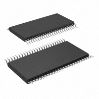


 工商网监
湘ICP备2023018690号
工商网监
湘ICP备2023018690号
