Product
Folder
Order
Now
Support &
Community
Tools &
Software
Technical
Documents
DAC80501, DAC70501, DAC60501
SBAS794D – NOVEMBER 2018 – REVISED FEBRUARY 2020
DACx0501 16-Bit, 14-Bit, and 12-Bit, 1-LSB INL, Voltage-Output DACs
With Precision Internal Reference
1 Features
3 Description
•
•
•
•
•
•
The 16-bit DAC80501, 14-bit DAC70501, and 12-bit
DAC60501 (DACx0501) digital-to-analog converters
(DACs) are highly accurate, low-power devices with
voltage-output. The DACx0501 are specified
monotonic by design, and offer linearity of < 1 LSB.
These devices include a 2.5-V, 5-ppm/˚C internal
reference, giving full-scale output voltage ranges of
1.25 V, 2.5 V, or 5 V. The DACx0501 incorporate a
power-on-reset circuit that makes sure the DAC
output powers up at zero scale or midscale, and
remains at that scale until a valid code is written to
the device. These devices consume a low current of
1 mA, and include a power-down feature that reduces
current consumption to typically 15 µA at 5 V.
1
•
•
•
•
•
16-bit performance: 1-LSB INL and DNL (max)
Low glitch energy: 4 nV–s
Wide power supply: 2.7 V to 5.5 V
Buffered output range: 5 V, 2.5 V, or 1.25 V
Very-low power: 1 mA at 5.5 V
Integrated 5-ppm/˚C (max), 2.5-V precision
reference
Pin-selectable serial interface:
– 3-wire, SPI compatible up to 50-MHz
– 2-wire, I2C compatible
Power-on-reset: Zero scale or midscale
1.62-V VIH with VDD = 5.5 V
Temperature range: –40˚C to +125˚C
Packages: Small 8-Pin WSON and 10-Pin VSSOP
2 Applications
•
•
•
•
•
•
•
•
Oscilloscope (DSO)
Semiconductor test
Data acquisition (DAQ)
LCD test
Small cell base station
Analog output module
Process analytics (pH, gas, concentration, force
and humidity)
DC power supply, ac source, electronic load
The digital interface of the DACx0501 can be
configured to SPI or I2C mode using the SPI2C pin.
In SPI mode, the DACx0501 use a versatile 3-wire
serial interface that operates at clock rates of up to
50 MHz. In I2C mode, the DACx0501 operate in
standard (100 kbps), fast (400 kbps), and fast+
(1.0 Mbps) modes.
The DACx0501 are available in easy-to-assemble
10-pin VSSOP and small 2-mm × 2-mm, 8-pin WSON
packages. The devices are fully specified over the
industrial temperature range of –40°C to +125°C.
Device Information(1)
PART NUMBER
DAC80501
DAC70501
DAC60501
PACKAGE
BODY SIZE (NOM)
WSON (8)
2.00 mm × 2.00 mm
VSSOP (10)
3.00 mm × 3.00 mm
(1) For all available packages, see the package option addendum
at the end of the data sheet.
Functional Block Diagram
Offset Trimming With the DACx0501
VREFIO
VDD
Sign al
Input
SPI2C
SCLK or SCL
SDIN or SDA
OPA MP
Ser ial
Inte rface
DAC
Buffer
DAC
Registe r
DAC
BUF
DACx050 1
OPA MP
+
+
VOUT
Sign al
Output
±
±
VREFIO
Bipo lar
Output
R2
Power Down Logic
RG3
Power On Reset
RG1
SYNC or A0
Inte rface Logi c
Inte rnal
Reference
Resistive Network
AGND
1
An IMPORTANT NOTICE at the end of this data sheet addresses availability, warranty, changes, use in safety-critical applications,
intellectual property matters and other important disclaimers. PRODUCTION DATA.
�DAC80501, DAC70501, DAC60501
SBAS794D – NOVEMBER 2018 – REVISED FEBRUARY 2020
www.ti.com
Table of Contents
1
2
3
4
5
6
7
Features ..................................................................
Applications ...........................................................
Description .............................................................
Revision History.....................................................
Device Comparison Table.....................................
Pin Configuration and Functions .........................
Specifications.........................................................
7.1
7.2
7.3
7.4
7.5
7.6
7.7
7.8
7.9
7.10
8
1
1
1
2
3
3
4
Absolute Maximum Ratings ...................................... 4
ESD Ratings.............................................................. 4
Recommended Operating Conditions....................... 4
Thermal Information .................................................. 5
Electrical Characteristics........................................... 5
Timing Requirements : SPI Mode ............................. 9
Timing Requirements : I2C Standard Mode .............. 9
Timing Requirements : I2C Fast Mode...................... 9
Timing Requirements : I2C Fast-Mode Plus ........... 10
Typical Characteristics .......................................... 11
Detailed Description ............................................ 20
8.1 Overview ................................................................. 20
8.2 Functional Block Diagram ....................................... 20
8.3
8.4
8.5
8.6
9
Feature Description.................................................
Device Functional Modes........................................
Programming...........................................................
Register Map...........................................................
20
23
23
31
Application and Implementation ........................ 35
9.1 Application Information............................................ 35
9.2 Typical Application .................................................. 35
10 Power Supply Recommendations ..................... 38
11 Layout................................................................... 38
11.1 Layout Guidelines ................................................. 38
11.2 Layout Example .................................................... 38
12 Device and Documentation Support ................. 39
12.1
12.2
12.3
12.4
12.5
12.6
12.7
Documentation Support .......................................
Related Links ........................................................
Receiving Notification of Documentation Updates
Support Resources ...............................................
Trademarks ...........................................................
Electrostatic Discharge Caution ............................
Glossary ................................................................
39
39
39
39
39
39
39
13 Mechanical, Packaging, and Orderable
Information ........................................................... 39
4 Revision History
NOTE: Page numbers for previous revisions may differ from page numbers in the current version.
Changes from Revision C (November 2019) to Revision D
Page
•
Changed Figure 29 to remove broken text from x axis (typo).............................................................................................. 15
•
Changed Figures 33, 34 and 35; updated for clarity ............................................................................................................ 16
Changes from Revision B (August 2019) to Revision C
Page
•
Changed DGS (VSSOP) package from preview to production data (active) ......................................................................... 1
•
Added TUE parameter for DGS package to electrical characteristics table........................................................................... 5
•
Added gain error parameter for DGS package to electrical characteristics table .................................................................. 5
•
Added full-scale error parameter for DGS package to electrical characteristics table........................................................... 6
Changes from Revision A (August 2019) to Revision B
•
Page
Changed DAC70501 and DAC60501 devices from preview to production data (active)....................................................... 1
Changes from Original (November 2018) to Revision A
•
2
Page
Changed DAC80501 in DQF (WSON) package from advanced information (preview) to production data (active) ............. 1
Submit Documentation Feedback
Copyright © 2018–2020, Texas Instruments Incorporated
Product Folder Links: DAC80501 DAC70501 DAC60501
�DAC80501, DAC70501, DAC60501
www.ti.com
SBAS794D – NOVEMBER 2018 – REVISED FEBRUARY 2020
5 Device Comparison Table
DEVICE
RESOLUTION
REFERENCE
POWER-ON RESET
DAC80501Z
16-Bit
Internal (default) or External
Zero Scale
DAC80501M
16-Bit
Internal (default) or External
Midscale
Zero Scale
DAC70501Z
14-Bit
Internal (default) or External
DAC70501M
14-Bit
Internal (default) or External
Midscale
DAC60501Z
12-Bit
Internal (default) or External
Zero Scale
DAC60501M
12-Bit
Internal (default) or External
Midscale
6 Pin Configuration and Functions
DGS Package
10-Pin VSSOP
Top View
DQF Package
8-Pin WSON
Top View
VDD
1
10
VREFIO
VOUT
2
9
NC
NC
3
8
SDIN/SDA
AGND
4
7
SYNC/A0
SPI2C
5
6
SCLK/SCL
VDD
1
8
VREFIO
VOUT
2
7
SDIN/SDA
AGND
3
6
SYNC/A0
SPI2C
4
5
SCLK/SCL
Not to scale
Not to scale
Pin Functions
PIN
DQF
TYPE
DESCRIPTION
NAME
DGS
AGND
4
3
Ground
NC
3
—
—
No connection. Leave floating.
NC
9
—
—
No connection. Leave floating.
SCLK/SCL
6
5
Input
Ground reference point for all circuitry on the device.
Serial interface clock. SPI or I2C mode.
SPI mode: Serial interface data input. Data are clocked into the input shift
register on each falling edge of the SCLK pin.
Input/output I2C mode: Data are clocked into or out of the input register. This pin is a
bidirectional, SDA drain data line that must be connected to the supply voltage
with an external pullup resistor.
SDIN/SDA
8
7
SPI2C
5
4
Input
Interface select pin.
Digital interface in SPI mode if SPI2C = 0
Digital interface in I2C mode if SPI2C = 1
SPI2C pin must be kept static after device powers up.
SYNC/A0
7
6
Input
SPI mode: Active low serial data enable. This input is the frame synchronization
signal for the serial data. When the signal goes low, the serial interface input
shift register is enabled.
I2C mode: Four-state address input 0.
VDD
1
1
Power
Analog supply voltage (2.7 V to 5.5 V)
VOUT
2
2
Output
Analog output voltage from the DAC
VREFIO
10
8
Input/output
When using the internal reference, this pin is the reference output voltage pin
(default). Reference input to the device when operating with external reference.
Copyright © 2018–2020, Texas Instruments Incorporated
Product Folder Links: DAC80501 DAC70501 DAC60501
Submit Documentation Feedback
3
�DAC80501, DAC70501, DAC60501
SBAS794D – NOVEMBER 2018 – REVISED FEBRUARY 2020
www.ti.com
7 Specifications
7.1 Absolute Maximum Ratings
over operating free-air temperature range (unless otherwise noted) (1)
MIN
MAX
VDD to AGND
–0.3
6
VREFIO to AGND
–0.3
VDD + 0.3
Digital input(s) to AGND
–0.3
VDD + 0.3
Output voltage
VOUT to AGND
–0.3
VDD + 0.3
Input current
Current into any pin
–10
10
Junction temperature (TJ)
–40
150
Storage temperature (Tstg)
–65
150
Input voltage
Temperature
(1)
UNIT
V
V
mA
°C
Stresses beyond those listed under Absolute Maximum Ratings may cause permanent damage to the device. These are stress ratings
only, which do not imply functional operation of the device at these or any other conditions beyond those indicated under Recommended
Operating Conditions. Exposure to absolute-maximum-rated conditions for extended periods may affect device reliability.
7.2 ESD Ratings
VALUE
V(ESD)
(1)
(2)
Electrostatic discharge
Human body model (HBM), per ANSI/ESDA/JEDEC JS001, all pins (1)
±2000
Charged device model (CDM), per JEDEC specification
JESD22-C101, all pins (2)
±1000
UNIT
V
JEDEC document JEP155 states that 500-V HBM allows safe manufacturing with a standard ESD control process.
JEDEC document JEP157 states that 250-V CDM allows safe manufacturing with a standard ESD control process.
7.3 Recommended Operating Conditions
over operating free-air temperature range (unless otherwise noted)
MIN
NOM
MAX
UNIT
POWER SUPPLY
VDD to AGND
Positive supply voltage to ground
2.7
5.5
V
DIGITAL INPUTS
VIH
Input high voltage
VIL
Input low voltage
1.62
V
0.45
V
REFERENCE INPUT
VREFIO to AGND
2.7 V ≤ VDD < 3.3 V,
reference divider disabled (REF-DIV bit = 0)
1.2
0.5 × (VDD – 0.2)
V
VREFIO to AGND
2.7 V ≤ VDD < 3.3 V,
reference divider enabled (REF-DIV bit = 1)
2.4
(VDD – 0.2)
V
VREFIO to AGND
3.3 V ≤ VDD ≤ 5.5 V,
reference divider disabled (REF-DIV bit = 0)
1.2
0.5 × VDD
V
VREFIO to AGND
3.3 V ≤ VDD ≤ 5.5 V,
reference divider enabled (REF-DIV bit = 1)
2.4
VDD
V
Operating temperature
–40
125
°C
TEMPERATURE
TA
4
Submit Documentation Feedback
Copyright © 2018–2020, Texas Instruments Incorporated
Product Folder Links: DAC80501 DAC70501 DAC60501
�DAC80501, DAC70501, DAC60501
www.ti.com
SBAS794D – NOVEMBER 2018 – REVISED FEBRUARY 2020
7.4 Thermal Information
DACx0501
THERMAL METRIC (1)
DGS (VSSOP)
DQF (WSON)
10 PINS
8 PINS
UNIT
RθJA
Junction-to-ambient thermal resistance
170.1
122.6
°C/W
RθJC(top)
Junction-to-case (top) thermal resistance
60.5
58.3
°C/W
RθJB
Junction-to-board thermal resistance
92.6
50
°C/W
ΨJT
Junction-to-top characterization parameter
7.8
1.5
°C/W
ΨJB
Junction-to-board characterization parameter
90.7
49.8
°C/W
(1)
For more information about traditional and new thermal metrics, see the Semiconductor and IC Package Thermal Metrics application
report.
7.5 Electrical Characteristics
all minimum and maximum values at TA = –40°C to +125°C and all typcal values at TA = 25°C, 2.7 V ≤ VDD ≤ 5.5 V, external
or internal VREFIO = 1.25 V to 5.5 V , RLOAD = 2 kΩ to AGND, CLOAD = 200 pF to AGND, and digital inputs at VDD or AGND
(unless otherwise noted)
PARAMETER
TEST CONDITIONS
MIN
TYP
MAX
UNIT
STATIC PERFORMANCE
Resolution
DAC80501
16
DAC70501
14
DAC60501
12
Bits
INL
Integral nonlinearity (1)
–1
1
LSB
DNL
Differential nonlinearity (1)
–1
1
LSB
TUE
Total unadjusted error (1)
Zero code error (1)
DAC80501,
reference divider disabled (REF-DIV bit = 0)
–0.08
-0.02
0.08
DAC80501,
reference divider enabled (REF-DIV bit = 1)
–0.06
0.025
0.06
DAC80501, DGS package
reference divider enabled (REF-DIV bit = 1)
–0.07
0.025
0.07
DAC70501, DAC60501
–0.1
0.04
0.1
DAC loaded with zero scale code
–1.5
0.5
1.5
Zero code error temperature
coefficient (1)
Offset error
±2
(1)
–1.5
Offset error temperature
coefficient (1)
Gain error (1)
1.5
–0.08
-0.02
0.08
DAC80501,
reference divider enabled (REF-DIV bit = 1)
–0.06
0.025
0.06
DAC80501, DGS package
reference divider enabled (REF-DIV bit = 1)
–0.07
0.025
0.07
–0.1
0.04
0.1
±1
mV
µV/°C
DAC80501,
reference divider disabled (REF-DIV bit = 0)
Gain error temperature
coefficient (1)
mV
µV/°C
±2
DAC70501, DAC60501
(1)
0.5
%FSR
%FSR
ppm
FSR/°C
End point fit between code 256 to code 64,511 for 16-bit, code 64 to code 16,127 for 14-bit, code 16 to code 4031 for 12 bit, DAC output
unloaded, performance under resistive and capacitice load conditions are specified by design and characterization, DAC output range ≥
2.5 V.
Copyright © 2018–2020, Texas Instruments Incorporated
Product Folder Links: DAC80501 DAC70501 DAC60501
Submit Documentation Feedback
5
�DAC80501, DAC70501, DAC60501
SBAS794D – NOVEMBER 2018 – REVISED FEBRUARY 2020
www.ti.com
Electrical Characteristics (continued)
all minimum and maximum values at TA = –40°C to +125°C and all typcal values at TA = 25°C, 2.7 V ≤ VDD ≤ 5.5 V, external
or internal VREFIO = 1.25 V to 5.5 V , RLOAD = 2 kΩ to AGND, CLOAD = 200 pF to AGND, and digital inputs at VDD or AGND
(unless otherwise noted)
PARAMETER
TEST CONDITIONS
Full-scale error (1)
MIN
TYP
MAX
DAC80501, DAC loaded with full scale,
reference divider disabled (REF-DIV bit = 0)
–0.08
-0.02
0.08
DAC80501, DAC loaded with full scale,
reference divider enabled (REF-DIV bit = 1)
–0.06
0.025
0.06
DAC80501, DGS package
reference divider enabled (REF-DIV bit = 1)
–0.07
0.025
0.07
–0.1
0.04
0.1
DAC70501, DAC60501
Full-scale error temperature
coefficient (1)
UNIT
%FSR
ppm
FSR/°C
±2
OUTPUT CHARACTERISTICS
VO
Output voltage
BUFF-GAIN bit set to 1, REF-DIV bit set to 0
0
2×
VREFIO
BUFF-GAIN bit set to 1, REF-DIV bit set to 1
0
VREFIO
0
0.5 ×
VREFIO
BUFF-GAIN bit set to 0, REF-DIV bit set to 1
RLOAD
Resistive load (2)
CLOAD
Capacitive load (2)
0.25
VDD = 5.5 V
0.5
kΩ
RLOAD = infinite
2
RLOAD = 2 kΩ
Load regulation
Short circuit current
ZO
VDD = 2.7 V
10
DAC at midscale, –10 mA ≤ IOUT ≤ 10 mA
80
Full scale output shorted to AGND
30
Zero output shorted to VDD
30
Output voltage headroom
to VDD, DAC at full code, IOUT = 10 mA
(sourcing)
0.3
Output voltage footroom
to AGND, DAC at zero code, IOUT = 10 mA
(sinking)
0.3
0.1
DAC at midscale
0.1
10
Power supply rejection ratio (DC)
Output voltage drift vs time
nF
µV/mA
mA
V
V
DC small signal output impedance DAC at code 256
DAC at code 65279
V
Ω
10
DAC at midscale; VDD = 5 V ± 10%
0.15
TA = 35°C, VOUT = midscale, 1900 hr
mV/V
20
ppm of
FSR
100
kΩ
5
pF
VOLTAGE REFERENCE INPUT
ZVREFIO
Reference input impedance
(VREFIO)
CVREFIO
Reference input capacitance
(VREFIO)
(2)
6
Not production tested.
Submit Documentation Feedback
Copyright © 2018–2020, Texas Instruments Incorporated
Product Folder Links: DAC80501 DAC70501 DAC60501
�DAC80501, DAC70501, DAC60501
www.ti.com
SBAS794D – NOVEMBER 2018 – REVISED FEBRUARY 2020
Electrical Characteristics (continued)
all minimum and maximum values at TA = –40°C to +125°C and all typcal values at TA = 25°C, 2.7 V ≤ VDD ≤ 5.5 V, external
or internal VREFIO = 1.25 V to 5.5 V , RLOAD = 2 kΩ to AGND, CLOAD = 200 pF to AGND, and digital inputs at VDD or AGND
(unless otherwise noted)
PARAMETER
TEST CONDITIONS
MIN
TYP
MAX
UNIT
VOLTAGE REFERENCE OUTPUT
Output (initial accuracy) (3)
TA = 25°C
2.4975
DAC80501
Output drift (3)
10
V
ppm/℃
0.1
(3)
0.1 Hz to 10 Hz
Output noise density (3)
Measured at 10 kHz, reference load = 10 nF
Load current (3)
Load regulation
5
DAC70501, DAC60501
Output impedance (3)
Output noise
2.5025
(3)
Sourcing and sinking
Line regulation (3)
Output voltage drift vs time (3)
TA = 35°C, 1900 hr
1st cycle
Thermal hysteresis (3)
Additional cycle
Ω
14
µVPP
140
nV/√Hz
±5
mA
90
µV/mA
20
µV/V
20
µV
500
µV
25
µV
DYNAMIC PERFORMANCE
ts
¼ to ¾ scale and ¾ to ¼ scale settling to ±2
LSB, VDD = 5.5 V, VREFIO = 2.5 V
5
10-mV settling to ±2 LSB, VDD = 5.5 V,
VREFIO = 2.5 V
3
Slew rate (4)
VDD = 5.5 V, VREFIO = 2.5 V
2
V/µs
Power on glitch magnitude
CLOAD = 50 pF
Output voltage settling time
(4)
Output noise (4)
Vn
Vn
Output noise density
µs
200
mV
0.1 Hz to 10 Hz, DAC at midscale,
VDD = 5.5 V, external VREFIO = 2.5 V
14
µVPP
100-kHz Bandwidth, DAC at midscale,
VDD = 5.5 V, external VREFIO = 2.5 V
23
µVrms
Measured at 1 kHz, DAC at midscale,
VDD = 5.5 V, external VREFIO = 2.5 V,
gain = 2X (BUFF-GAIN bit = 1)
78
Measured at 10 kHz, DAC at midscale,
VDD = 5.5 V, external VREFIO = 2.5 V,
gain = 2X (BUFF-GAIN bit = 1)
74
Measured at 1 kHz, DAC at full scale,
VDD = 2.7 V, external VREFIO = 2.5 V,
gain = 1X (BUFF-GAIN bit = 0)
55
Measured at 10 kHz, DAC at full scale,
VDD = 2.7 V, external VREFIO = 2.5 V,
gain = 1X (BUFF-GAIN bit = 0)
50
nV/√Hz
SFDR
Spurious free dynamic range
1-kHz sinusiod at DAC output, DAC updated
at 500 kHz, include up to 7th harmonics, no
filter on DAC output
70
dB
THD
Total harmonic distortion
1-kHz sinusiod at DAC output, DAC updated
at 500 kHz, include up to 7th harmonics, no
filter on DAC output
70
dB
Power supply rejection ratio (ac)
200-mV 50-Hz to 60-Hz sine wave
superimposed on power supply voltage, DAC
at midscale. (ac analysis)
85
dB
Code change glitch impulse
Midcode ±1 LSB (including feedthrough)
4
nV-s
Code change glitch magnitude
Midcode ±1 LSB (including feedthrough)
gain = 1X (BUFF-GAIN bit = 0)
7.5
mV
(3)
(4)
Characterized on 8-pin DQF package.
Output buffer in gain = 2X setting (BUFF-GAIN bit = 1).
Copyright © 2018–2020, Texas Instruments Incorporated
Product Folder Links: DAC80501 DAC70501 DAC60501
Submit Documentation Feedback
7
�DAC80501, DAC70501, DAC60501
SBAS794D – NOVEMBER 2018 – REVISED FEBRUARY 2020
www.ti.com
Electrical Characteristics (continued)
all minimum and maximum values at TA = –40°C to +125°C and all typcal values at TA = 25°C, 2.7 V ≤ VDD ≤ 5.5 V, external
or internal VREFIO = 1.25 V to 5.5 V , RLOAD = 2 kΩ to AGND, CLOAD = 200 pF to AGND, and digital inputs at VDD or AGND
(unless otherwise noted)
PARAMETER
Digital feedthrough
TEST CONDITIONS
MIN
At SCLK = 1 MHz, DAC output at midscale
TYP
MAX
4
UNIT
nV-s
DIGITAL INPUTS
Hysteresis voltage
0.4
Input current
Pin capacitance
–5
V
5
µA
Per pin
10
pF
Normal mode, internal reference enabled,
DAC at full scale, SPI static
1.5
2.0
Normal mode, external reference = 2.5 V,
DAC at full scale, SPI static
1
1.4
DAC and Internal reference power-down
15
µA
0-V to 5-V range, midscale code
25
µA
POWER REQUIREMENTS
IVDD
Current flowing into VDD
IVREFIO
Current flowing into VREFIO
8
Submit Documentation Feedback
mA
Copyright © 2018–2020, Texas Instruments Incorporated
Product Folder Links: DAC80501 DAC70501 DAC60501
�DAC80501, DAC70501, DAC60501
www.ti.com
SBAS794D – NOVEMBER 2018 – REVISED FEBRUARY 2020
7.6 Timing Requirements : SPI Mode
all input signals are specified with tR = tF = 1 ns/V and timed from a voltage level of (VIL + VIH) / 2. 2.7 V ≤ VDD ≤ 5.5 V,
VIH = 1.62 V, VIL = 0.15 V, VREFIO = 1.25 V to 5.5 V, and TA = –40°C to +125°C (unless otherwise noted)
MIN
NOM
MAX
UNIT
50
MHz
fSCLK
SCLK frequency
tSCLKHIGH
SCLK high time
9
ns
tSCLKLOW
SCLK low time
9
ns
tSDIS
SDIN setup
5
ns
tSDIH
SDIN hold
10
ns
tSYNCS
SYNC falling edge to SCLK falling edge setup
13
ns
tSYNCH
SCLK falling edge to SYNC rising edge
10
ns
tSYNCHIGH
SYNC high time
160
ns
tSYNCIGNOR
SCLK falling edge to SYNC ignore
15
ns
Sequential DAC update wait time
1
µs
E
tDACWAIT
7.7 Timing Requirements : I2C Standard Mode
all input signals are specified with tR = tF = 1 ns/V and timed from a voltage level of (VIL + VIH) / 2. 2.7 V ≤ VDD ≤ 5.5 V,
VIH = 1.62 V, VIL = 0.45 V, VREFIO = 1.25 V to 5.5 V, and TA = – 40°C to +125°C (unless otherwise noted)
MIN
fSCLK
SCL frequency
tBUF
Bus free time between stop and start conditions
tHDSTA
Hold time after repeated start
tSUSTA
NOM
MAX
UNIT
0.1
MHz
4.7
µs
4
µs
Repeated start setup time
4.7
µs
tSUSTO
Stop condition setup time
4
µs
tHDDAT
Data hold time
0
ns
tSUDAT
Data setup time
250
ns
tLOW
SCL clock low period
4700
ns
tHIGH
SCL clock high period
4000
tR
Clock and data fall time
300
ns
tF
Clock and data rise time
1000
ns
tUPDATE
Sequential DAC update wait time
ns
1
µs
7.8 Timing Requirements : I2C Fast Mode
all input signals are specified with tR = tF = 1 ns/V and timed from a voltage level of (VIL + VIH) / 2. 2.7 V ≤ VDD ≤ 5.5 V,
VIH = 1.62 V, VIL = 0.45 V, VREFIO = 1.25 V to 5.5 V, and TA = – 40°C to +125°C (unless otherwise noted)
MIN
NOM
MAX
UNIT
0.4
MHz
fSCLK
SCL frequency
tBUF
Bus free time between stop and start conditions
1.3
µs
tHDSTA
Hold time after repeated start
0.6
µs
tSUSTA
Repeated start setup time
0.6
µs
tSUSTO
Stop condition setup time
0.6
µs
tHDDAT
Data hold time
0
ns
tSUDAT
Data setup time
100
ns
tLOW
SCL clock low period
1300
ns
tHIGH
SCL clock high period
600
tR
Clock and data fall time
tF
Clock and data rise time
tUPDATE
Sequential DAC update wait time
ns
300
300
Copyright © 2018–2020, Texas Instruments Incorporated
Product Folder Links: DAC80501 DAC70501 DAC60501
1
Submit Documentation Feedback
ns
ns
µs
9
�DAC80501, DAC70501, DAC60501
SBAS794D – NOVEMBER 2018 – REVISED FEBRUARY 2020
www.ti.com
7.9 Timing Requirements : I2C Fast-Mode Plus
all input signals are specified with tR = tF = 1 ns/V and timed from a voltage level of (VIL + VIH) / 2. 2.7 V ≤ VDD ≤ 5.5 V,
VIH = 1.62 V, VIL = 0.45 V, VREFIO = 1.25 V to 5.5 V, and TA = – 40°C to +125°C (unless otherwise noted)
MIN
fSCLK
SCL frequency
tBUF
Bus free time between stop and start conditions
tHDSTA
NOM
MAX
UNIT
1
MHz
0.5
µs
Hold time after repeated start
0.26
µs
tSUSTA
Repeated start setup time
0.26
µs
tSUSTO
Stop condition setup time
0.26
µs
tHDDAT
Data hold time
0
ns
tSUDAT
Data setup time
50
ns
tLOW
SCL clock low period
500
ns
tHIGH
SCL clock high period
260
tR
Clock and data fall time
tF
Clock and data rise time
tUPDATE
Sequential DAC update wait time
ns
120
120
1
ns
ns
µs
tSYNC HIGH
tSYNC H
tSYNC S
SYNC
tSYNC IGN OR E
tSCL KLOW
SCLK
tSCL KHIGH
SDIN
Bit 23
tSDIS
Bit 1
Bit 0
tSDIH
Figure 1. SPI Mode Timing
Low byte ACK cycle
tLOW
tR
tF
SCL
tHD STA
tHIGH
tHD DAT
tSUSTA
tSUSTO
tSUD AT
tHD STA
SDA
tBUF
P
S
S
P
Figure 2. I2C Mode Timing
10
Submit Documentation Feedback
Copyright © 2018–2020, Texas Instruments Incorporated
Product Folder Links: DAC80501 DAC70501 DAC60501
�DAC80501, DAC70501, DAC60501
www.ti.com
SBAS794D – NOVEMBER 2018 – REVISED FEBRUARY 2020
7.10 Typical Characteristics
at TA = 25°C, VDD = 5.5 V, Internal reference = 2.5 V, REF-DIV = 0 and BUFF-GAIN = 1, and DAC outputs unloaded (unless
otherwise noted)
1
1
Unloaded
5 k: || 200 pF
0.6
0.6
0.4
0.4
0.2
0
-0.2
0.2
0
-0.2
-0.4
-0.4
-0.6
-0.6
-0.8
-0.8
-1
-1
0
0
8192 16384 24576 32768 40960 49152 57344 65536
Code
D001
Figure 3. Integral Linearity Error vs Digital Input Code
1
Unloaded
5 k: || 200 pF
0.06
0.5
0.02
0.25
INL (LSB)
0.04
0
-0.02
0
-0.25
-0.04
-0.5
-0.06
-0.75
0
-1
-40
8192 16384 24576 32768 40960 49152 57344 65536
Code
D003
Figure 5. Total Unadjusted Error vs Digital Input Code
-25
-10
5
20 35 50 65
Temperature (oC)
80
95
110 125
D004
Figure 6. Integral Linearity Error vs Temperature
1
0.08
0.5
Total Unadjusted Error (%FSR)
DNL Max, Unloaded
DNL Min, Unloaded
DNL Max, 5 k: || 200 pF
DNL Min, 5 k: || 200 pF
0.75
0.25
0
-0.25
-0.5
-0.75
-1
-40
INL Max, Unloaded
INL Min, Unloaded
INL Max, 5 k: || 200 pF
INL Min, 5 k: || 200 pF
0.75
-0.08
DNL (LSB)
8192 16384 24576 32768 40960 49152 57344 65536
Code
D002
Figure 4. Differential Linearity Error vs Digital Input Code
0.08
Total Unadjusted Error (%FSR)
Unloaded
5 k: || 200 pF
0.8
DNL (LSB)
INL (LSB)
0.8
-25
-10
5
20 35 50 65
Temperature (oC)
80
95
110 125
Unloaded
5 k: || 200 pF
0.06
0.04
0.02
0
-0.02
-0.04
-0.06
-0.08
-40
-25
-10
5
D005
Figure 7. Differential Linearity Error vs Temperature
20 35 50 65
Temperature (oC)
80
95
110 125
D006
Figure 8. Total Unadjusted Error vs Temperature
Copyright © 2018–2020, Texas Instruments Incorporated
Product Folder Links: DAC80501 DAC70501 DAC60501
Submit Documentation Feedback
11
�DAC80501, DAC70501, DAC60501
SBAS794D – NOVEMBER 2018 – REVISED FEBRUARY 2020
www.ti.com
Typical Characteristics (continued)
1.5
1.5
1.25
1
Offset Error (mV)
Zero Code Error (mV)
at TA = 25°C, VDD = 5.5 V, Internal reference = 2.5 V, REF-DIV = 0 and BUFF-GAIN = 1, and DAC outputs unloaded (unless
otherwise noted)
1
0.75
0.5
0.5
0
-0.5
-1
0.25
0
-40
-25
-10
5
20 35 50 65
Temperature (oC)
80
95
-1.5
-40
110 125
80
95
110 125
D008
Unloaded
5 k: || 200 pF
0.04
0.04
Gain Error (%FSR)
Full Scale Error (%FSR)
20 35 50 65
Temperature (oC)
0.06
0.02
0
-0.02
0.02
0
-0.02
-0.04
-0.04
-0.06
-0.06
-25
-10
5
20 35 50 65
Temperature (oC)
80
95
-0.08
-40
110 125
-25
-10
5
D009
Data
Figure 11. Full Scale Error vs Temperature
20 35 50 65
Temperature (oC)
80
95
110 125
D010
Figure 12. Gain Error vs Temperature
1
1
Max INL
Min INL
0.75
0.5
0.5
0.25
0.25
0
-0.25
0
-0.25
-0.5
-0.5
-0.75
-0.75
3.1
3.5
3.9
4.3
VDD (V)
4.7
5.1
5.5
-1
2.7
3.1
3.5
D011
REF-DIV = 0 and BUFF-GAIN = 0
Figure 13. Integral Linearity Error vs Supply Voltage
Submit Documentation Feedback
Max DNL
Min DNL
0.75
DNL (LSB)
INL (LSB)
5
0.08
Unloaded
5 k: || 200 pF
0.06
12
-10
Figure 10. Offset Error vs Temperature
0.08
-1
2.7
-25
D007
Figure 9. Zero Code Error vs Temperature
-0.08
-40
Unloaded
5 k: || 200 pF
3.9
4.3
VDD (V)
4.7
5.1
5.5
D012
REF-DIV = 0 and BUFF-GAIN = 0
Figure 14. Differential Linearity Error vs Supply Voltage
Copyright © 2018–2020, Texas Instruments Incorporated
Product Folder Links: DAC80501 DAC70501 DAC60501
�DAC80501, DAC70501, DAC60501
www.ti.com
SBAS794D – NOVEMBER 2018 – REVISED FEBRUARY 2020
Typical Characteristics (continued)
at TA = 25°C, VDD = 5.5 V, Internal reference = 2.5 V, REF-DIV = 0 and BUFF-GAIN = 1, and DAC outputs unloaded (unless
otherwise noted)
1.5
REF-DIV = 1, BUFF-GAIN = 1
REF-DIV = 0, BUFF-GAIN = 0
0.06
0.04
0.02
0
-0.02
-0.04
0.5
0
-0.5
-1
-0.06
-0.08
2.7
REF-DIV = 1, BUFF-GAIN = 1
REF-DIV = 0, BUFF-GAIN = 0
1
Zero Code Error (mV)
Total Unadjusted Error (%FSR)
0.08
3.1
3.5
3.9
4.3
VDD (V)
4.7
5.1
-1.5
2.7
5.5
3.1
3.5
3.9
4.3
VDD (V)
D013
Figure 15. Total Unadjusted Error vs Supply Voltage
4.7
5.1
5.5
D014
Figure 16. Zero Code Error vs Supply Voltage
0.08
1.5
REF-DIV = 1, BUFF-GAIN = 1
REF-DIV = 0, BUFF-GAIN = 0
1
REF-DIV = 1, BUFF-GAIN = 1
REF-DIV = 0, BUFF-GAIN = 0
0.06
Gain Error (%FSR)
Offset Error (mV)
0.04
0.5
0
-0.5
0.02
0
-0.02
-0.04
-1
-1.5
2.7
-0.06
3.1
3.5
3.9
4.3
VDD (V)
4.7
5.1
-0.08
2.7
5.5
Figure 17. Offset Error vs Supply Voltage
3.9
4.3
VDD (V)
4.7
5.1
5.5
D016
1
REF-DIV = 1, BUFF-GAIN = 1
REF-DIV = 0, BUFF-GAIN = 0
0.06
0.04
0.5
0.02
0.25
0
-0.02
0
-0.25
-0.04
-0.5
-0.06
-0.75
3.1
3.5
3.9
4.3
VDD (V)
4.7
5.1
Figure 19. Full Scale Error vs Supply Voltage
Max, REFDIV = 0
Max, REFDIV = 1
Min, REFDIV = 0
Min, REFDIV = 1
0.75
INL (LSB)
Full Scale Error (%FSR)
3.5
Figure 18. Gain Error vs Supply Voltage
0.08
-0.08
2.7
3.1
D015
5.5
-1
1.25
2
2.75
D017
3.5
VREFIN (V)
4.25
5
5.5
D018
Figure 20. Integral Linearity Error vs Reference Voltage
Copyright © 2018–2020, Texas Instruments Incorporated
Product Folder Links: DAC80501 DAC70501 DAC60501
Submit Documentation Feedback
13
�DAC80501, DAC70501, DAC60501
SBAS794D – NOVEMBER 2018 – REVISED FEBRUARY 2020
www.ti.com
Typical Characteristics (continued)
at TA = 25°C, VDD = 5.5 V, Internal reference = 2.5 V, REF-DIV = 0 and BUFF-GAIN = 1, and DAC outputs unloaded (unless
otherwise noted)
1
0.08
0.75
DNL (LSB)
0.5
Total Unadjusted Error (%FSR)
Max, REFDIV = 0
Max, REFDIV = 1
Min, REFDIV = 0
Min, REFDIV = 1
0.25
0
-0.25
-0.5
-0.75
-1
1.25
2
2.75
3.5
VREFIN (V)
4.25
5
0.04
0.02
0
-0.02
-0.04
-0.06
-0.08
1.25
5.5
3.5
VREFIN (V)
4.25
5
5.5
D020
1.5
REF-DIV = 0, BUFF-GAIN = 0
REF-DIV = 1, BUFF-GAIN = 1
REF-DIV = 0, BUFF-GAIN = 0
REF-DIV = 1, BUFF-GAIN = 1
1
Offset Error (mV)
1
0.5
0
-0.5
0.5
0
-0.5
-1
-1
-1.5
1.25
2
2.75
3.5
VREFIN (V)
4.25
5
-1.5
1.25
5.5
2.75
3.5
VREFIN (V)
4.25
5
5.5
D022
Figure 24. Offset Error vs Reference Voltage
0.08
0.08
REF-DIV = 0, BUFF-GAIN = 0
REF-DIV = 1, BUFF-GAIN = 1
0.06
REF-DIV = 0, BUFF-GAIN = 0
REF-DIV = 1, BUFF-GAIN = 1
0.06
Zero Code Error (mV)
0.04
0.02
0
-0.02
-0.04
-0.06
-0.08
1.25
2
D021
Figure 23. Zero Code Error vs Reference Voltage
Zero Code Error (mV)
2.75
Figure 22. Total Unadjusted Error vs Reference Voltage
1.5
0.04
0.02
0
-0.02
-0.04
-0.06
2
2.75
3.5
VREFIN (V)
4.25
5
Figure 25. Gain Error vs Reference Voltage
14
2
D019
Figure 21. Differential Linearity Error vs Reference Voltage
Zero Code Error (mV)
REFDIV = 0
REFDIV = 1
0.06
Submit Documentation Feedback
5.5
-0.08
1.25
2
2.75
D023
3.5
VREFIN (V)
4.25
5
5.5
D024
Figure 26. Full Scale Error vs Reference Voltage
Copyright © 2018–2020, Texas Instruments Incorporated
Product Folder Links: DAC80501 DAC70501 DAC60501
�DAC80501, DAC70501, DAC60501
www.ti.com
SBAS794D – NOVEMBER 2018 – REVISED FEBRUARY 2020
Typical Characteristics (continued)
2
2
1.75
1.75
1.5
1.5
1.25
1.25
IDD (mA)
IDD (mA)
at TA = 25°C, VDD = 5.5 V, Internal reference = 2.5 V, REF-DIV = 0 and BUFF-GAIN = 1, and DAC outputs unloaded (unless
otherwise noted)
1
0.75
1
0.75
0.5
0.5
Internal Reference, BUFF-GAIN = 0
Internal Reference, BUFF-GAIN = 1
External Reference, BUFF-GAIN = 0
External Reference, BUFF-GAIN = 1
0.25
0.25
0
0
Internal Reference, BUFF-GAIN = 0
Internal Reference, BUFF-GAIN = 1
External Reference, BUFF-GAIN = 0
External Reference, BUFF-GAIN = 1
0
-40
8192 16384 24576 32768 40960 49152 57344 65536
Code
D025
-25
-10
5
20 35 50 65
Temperature (qC)
80
95
110 125
D026
DAC code at midscale
Figure 27. Supply Current vs Digital Input Code
Figure 28. Supply Current vs Temperature
2
12
Internal Reference, BUFF-GAIN = 0
Internal Reference, BUFF-GAIN = 1
External Reference, BUFF-GAIN = 0
External Reference, BUFF-GAIN = 1
1.75
10
8
1.25
IDD (P$)
IDD (mA)
1.5
1
0.75
6
4
0.5
2
0.25
0
2.7
3.1
3.5
3.9
4.3
VDD (V)
4.7
5.1
0
-40
5.5
-25
-10
5
20 35 50 65
Temperature (qC)
D027
DAC code at midscale
80
95
110 125
D028
REF-DIV = 0 and BUFF-GAIN = 0
Figure 29. Supply Current vs Supply Voltage
Figure 30. Power Down Current vs Temperature
1
15
0.8
0.6
12
'VOUT (V)
IDD (PA)
0.4
9
6
0.2
0
-0.2
-0.4
Sourcing 5.5V
Sourcing 2.7V
Sinking 5.5V
Sinking 2.7V
-0.6
3
-0.8
0
2.7
-1
3.1
3.5
3.9
4.3
VDD (V)
4.7
5.1
5.5
D029
External reference = 2.5 V, REF-DIV = 1 and BUFF-GAIN = 0
Figure 31. Power Down Current vs Supply Voltage
0
5
10
15
20
Load Current (mA)
25
30
D033
External reference = 2.5 V
Figure 32. Headroom and Footroom vs Load Current
Copyright © 2018–2020, Texas Instruments Incorporated
Product Folder Links: DAC80501 DAC70501 DAC60501
Submit Documentation Feedback
15
�DAC80501, DAC70501, DAC60501
SBAS794D – NOVEMBER 2018 – REVISED FEBRUARY 2020
www.ti.com
Typical Characteristics (continued)
at TA = 25°C, VDD = 5.5 V, Internal reference = 2.5 V, REF-DIV = 0 and BUFF-GAIN = 1, and DAC outputs unloaded (unless
otherwise noted)
7
8
0xFFFF
0xC000
0x8000
0x4000
0x0
DAC Output (V)
5
0xFFFF
0xC000
0x8000
7
6
DAC Output (V)
6
4
3
2
1
0x4000
0x0
5
4
3
2
1
0
0
-1
-50
-40
-30
-20 -10
0
10
20
Loading Current (mA)
30
40
50
D031
REF-DIV = 0 and BUFF-GAIN = 0
-1
-50
-40
-30
-20 -10
0
10
20
Loading Current (mA)
30
40
50
D032
REF-DIV = 0 and BUFF-GAIN = 1
Figure 33. Source and Sink Capability
Figure 34. Source and Sink Capability
7
0xFFFF
0xC000
0x8000
0x4000
0x0
6
DAC Output (V)
5
4
3
3 nV-sec
2
1
VOUT (2.5 mV/div)
CS (5 V/div)
0
-1
-50
-40
-30
-20 -10
0
10
20
Loading Current (mA)
30
40
50
Time (0.5 Ps/div)
D034
D033
DAC code transition from midscale – 1 to midscale LSB,
REF-DIV = 0 and BUFF-GAIN = 0
REF-DIV = 1 and BUFF-GAIN = 0
Figure 36. Glitch Impulse, Rising Edge, 1 LSB Step
Figure 35. Source and Sink Capability
Small Singal VOUT (3 LSB/div)
Large Singal VOUT (2 V/div)
CS (5 V/div)
2 nV-sec
VOUT (2.5mV/div)
CS (5 V/div)
Time (0.5 Ps/div)
Time (2 Psec/div)
D035
DAC code transition from midscale to midscale – 1 LSB,
REF-DIV = 0 and BUFF-GAIN = 0
Figure 37. Glitch Impulse, Falling Edge, 1 LSB Step
16
Submit Documentation Feedback
D036
REF-DIV = 0 and BUFF-GAIN = 0
Figure 38. Full-Scale Settling Time, Rising Edge
Copyright © 2018–2020, Texas Instruments Incorporated
Product Folder Links: DAC80501 DAC70501 DAC60501
�DAC80501, DAC70501, DAC60501
www.ti.com
SBAS794D – NOVEMBER 2018 – REVISED FEBRUARY 2020
Typical Characteristics (continued)
at TA = 25°C, VDD = 5.5 V, Internal reference = 2.5 V, REF-DIV = 0 and BUFF-GAIN = 1, and DAC outputs unloaded (unless
otherwise noted)
VDD (2 V/div)
DAC Output (40 mV/div)
Small Singal VOUT (3 LSB/div)
Large Singal VOUT (2 V/div)
CS (5 V/div)
Time (1 ms/div)
Time (2 Psec/div)
D037
D038
REF-DIV = 0 and BUFF-GAIN = 0
REF-DIV = 0 and BUFF-GAIN = 0
Figure 39. Full-Scale Settling Time, Falling Edge
Figure 40. Power-on Glitch
0
VDD (2 V/div)
DAC Output (40 mV/div)
-10
-20
AC PSRR (dB)
-30
-40
-50
-60
-70
-80
-90
-100
-110
-120
Time (1 ms/div)
1
10
100
1000
Frequency (Hz)
D039
REF-DIV = 0 and BUFF-GAIN = 0
10000
100000
D040
DAC code at midscale, VDD = 5.0 V + 0.2 VPP,
REF-DIV = 0 and BUFF-GAIN = 0
Figure 41. Power-off Glitch
Figure 42. DAC Output AC PSRR vs Frequency
20
300
0
DAC Code = 0x0
DAC Code = 0x8000
DAC Code = 0xFFFF
250
Noise (nV/—Hz)
Noise (dB)
-20
-40
-60
-80
200
150
100
-100
50
-120
-140
0
4000
8000
12000
Frequency (Hz)
16000
20000
D041
fo = 1 kHz, fs = 400 kHz, includes 7 harmonics,
measurement bandwidth = 20 kHz, external reference = 2.5 V,
REF-DIV = 0 and BUFF-GAIN = 0
Figure 43. DAC Output THD+N vs Frequency
0
10 2030 50 100 200
5001000
Frequency (Hz)
10000
100000
D042
Gain = 1X (REF-DIV = 1 and BUFF-GAIN = 1),
external reference = 2.5 V,
REF-DIV = 0 and BUFF-GAIN = 0
Figure 44. DAC Output Noise Spectral Density
Copyright © 2018–2020, Texas Instruments Incorporated
Product Folder Links: DAC80501 DAC70501 DAC60501
Submit Documentation Feedback
17
�DAC80501, DAC70501, DAC60501
SBAS794D – NOVEMBER 2018 – REVISED FEBRUARY 2020
www.ti.com
Typical Characteristics (continued)
VNOISE (2 PV/div)
VNOISE (2 PV/div)
at TA = 25°C, VDD = 5.5 V, Internal reference = 2.5 V, REF-DIV = 0 and BUFF-GAIN = 1, and DAC outputs unloaded (unless
otherwise noted)
D043
D044
DAC code at midscale, external reference = 2.5 V,
REF-DIV = 0 and BUFF-GAIN = 0
DAC code at midscale, internal reference = 2.5 V,
REF-DIV = 0 and BUFF-GAIN = 0
Figure 45. DAC Output Noise 0.1 Hz to 10 Hz
Figure 46. DAC Output Noise 0.1 Hz to 10 Hz
2.505
Internal Reference (V)
SCLK (5 V/div)
VOUT (1 mV/div)
2.5025
2.5
2.4975
2.495
-40
Time (5 Psec/div)
-25
-10
5
D045
20 35 50 65
Temperature (oC)
SCLK = 1 MHz, DAC code at midscale, external reference = 2.5 V,
REF-DIV = 0 and BUFF-GAIN = 0
80
95
110 125
D046
30 units
Figure 47. Clock Feedthrough
Figure 48. Internal Reference Voltage vs Temperature
100
2.505
2.5025
Reference Drift (ppm)
Internal Refeence (V)
75
2.5
2.4975
50
25
0
-25
-50
-75
2.495
2.7
-100
3.1
3.5
3.9
4.3
VDD (V)
4.7
5.1
5.5
Figure 49. Internal Reference Voltage vs Supply Voltage
18
Submit Documentation Feedback
0
200
400
D047
600
800
Time (Hours)
1000
1200
D048
Figure 50. Internal Reference Voltage vs Time
Copyright © 2018–2020, Texas Instruments Incorporated
Product Folder Links: DAC80501 DAC70501 DAC60501
�DAC80501, DAC70501, DAC60501
www.ti.com
SBAS794D – NOVEMBER 2018 – REVISED FEBRUARY 2020
Typical Characteristics (continued)
at TA = 25°C, VDD = 5.5 V, Internal reference = 2.5 V, REF-DIV = 0 and BUFF-GAIN = 1, and DAC outputs unloaded (unless
otherwise noted)
800
700
VNOISE (2 PV/div)
Noise (nV/—Hz)
600
500
400
300
200
100
0
10 2030 50 100 200
5001000
Frequency (Hz)
10000
100000
D050
D049
Figure 52. Internal Reference Noise, 0.1 Hz to 10 Hz
Figure 51. Internal Reference Noise Density vs Frequency
55
100%
50
90%
45
80%
Percentage of Units
Number of Units
40
35
30
25
20
15
Presolder Heat Reflow
Postsolder Heat Reflow
70%
60%
50%
40%
30%
10
20%
5
10%
0
0
0
1
2
3
4
Temperature Drift (ppm/qC)
5
2.4975 2.4980 2.4985 2.4990 2.4995 2.5000 2.5005 2.5010
Figure 53. Internal Reference Temperature Drift Histogram
Percentage of Units
VREFOUT (V)
D051
D053
Figure 54. Internal Reference Initial Accuracy (Pre and Post
Solder) Histogram
28%
26%
24%
22%
20%
18%
16%
14%
12%
10%
8%
6%
4%
2%
0
-3 -2.5 -2 -1.5 -1 -0.5 0
0.5
1
1.5
VREFOUT Drift Delta (ppm/qC)
2
2.5
3
D054
Figure 55. Internal Reference Temperature Drift (Pre and Post Solder) Histogram
Copyright © 2018–2020, Texas Instruments Incorporated
Product Folder Links: DAC80501 DAC70501 DAC60501
Submit Documentation Feedback
19
�DAC80501, DAC70501, DAC60501
SBAS794D – NOVEMBER 2018 – REVISED FEBRUARY 2020
www.ti.com
8 Detailed Description
8.1 Overview
The DAC80501, DAC70501, DAC60501 (DACx0501) family of devices are buffered voltage output, 16-bit, 14-bit,
or 12-bit digital-to-analog converters (DACs), respectively. These devices include a 2.5-V, 5-ppm/˚C internal
reference, giving full-scale output voltage ranges of 1.25 V, 2.5 V, or 5 V. The DACx0501 devices incorporate a
power-on-reset circuit that makes sure that the DAC output powers up at zero scale or midscale, and remains at
that scale until a valid code is written to the device.
The digital interface of the DACx0501 can be configured to SPI or I2C mode using the SPI2C pin. In SPI mode,
the DACx0501 family uses a 3-wire serial interface that operates at clock rates up to 50 MHz. In I2C mode, the
DACx0501 devices operate in standard mode (100 kbps), fast mode (400 kbps), and fast mode plus (1.0 Mbps).
8.2 Functional Block Diagram
VREFIO
VDD
Inte rnal
Reference
Inte rface Logi c
SPI2C
SCLK or SCL
SDIN or SDA
DAC
Buffer
SYNC or A0
DAC
Registe r
BUF
DAC
VOUT
Power On Reset
Power Down Logic
Resistive Network
AGND
8.3 Feature Description
8.3.1 DAC Architecture
The output channel in the DACx0501 family of devices consists of a rail-to-rail ladder architecture with an output
buffer amplifier. The devices include an internal 2.5-V reference. Figure 56 shows a block diagram of the DAC
architecture.
2.5-V
Reference
VREFIO
REF Divider
(x1 or x0.5)
Serial Interface
DAC Data Register
DAC
Buffer
Register
REF-DIV Bit
BUFF-GAIN Bit
DAC
Active
Register
Gain
(x1 or x2)
VOUT
R-2R
BUF
DAC
Output
AGND
Figure 56. DACx0501 DAC Block Diagram
20
Submit Documentation Feedback
Copyright © 2018–2020, Texas Instruments Incorporated
Product Folder Links: DAC80501 DAC70501 DAC60501
�DAC80501, DAC70501, DAC60501
www.ti.com
SBAS794D – NOVEMBER 2018 – REVISED FEBRUARY 2020
Feature Description (continued)
8.3.1.1 DAC Transfer Function
The input data writes to the individual DAC data registers in straight binary format. After a power-on or a reset
event, all DAC registers are set to zero code (DACx0501Z devices) or midscale code (DACx0501M devices).
The DAC transfer function is shown by Equation 1.
VOUT
DAC_DATA
N
2
u
VREFIO
u GAIN
DIV
where:
•
•
•
•
•
N = resolution in bits = either 12 (DAC60501), 14 (DAC70501) or 16 (DAC80501).
DAC_DATA = decimal equivalent of the binary code that is loaded to the DAC register (address 8h).
DAC_DATA ranges from 0 to 2N – 1.
VREFIO = DAC reference voltage at the VREFIO pin. Either VREFIO from the internal 2.5-V reference or
VREFIO from an external reference.
DIV = 1 (default) or 2, as set by the REF-DIV bit in the GAIN register (address 4h).
GAIN = 1 or 2 (default), as set by the BUFF-GAIN bit in the GAIN register (address 4h).
(1)
8.3.1.2 DAC Register Structure
Data written to the DAC data registers are initially stored in the DAC buffer registers. The update mode of the
DAC output is determined by the status of the DAC_SYNC_EN bit (address 2h).
In asynchronous mode (default, DAC_SYNC_EN = 0), a write to the DAC buffer register results in an immediate
update of the DAC active register. In SPI mode, the DAC output (VOUT pin) updates on the rising edge of
SYNC. In I2C mode, the DAC output (VOUT pin) updates on the falling edge of SCL on the last acknowledge bit.
In synchronous mode (DAC_SYNC_EN = 1), writing to the DAC buffer register does not automatically update the
DAC active register. Instead, the update occurs only after a software LDAC trigger event. A software LDAC
trigger generates through the LDAC bit in the TRIGGER register (address 5h). When the host reads from a DAC
buffer register, the value held in the DAC buffer register is returned (not the value held in the DAC active
register).
8.3.1.3 Output Amplifier
The output buffer amplifier generates rail-to-rail voltages on the output, giving a maximum output range of 0 V to
VDD. Equation 1 shows that the full-scale output range of the DAC output is determined by the voltage on the
VREFIO pin, the reference divider setting (DIV) as set by the REF-DIV bit (address 4h), and the gain
configuration for that channel set by the corresponding BUFF-GAIN bit (address 4h).
8.3.2 Internal Reference
The DAx0501 family of devices includes a 2.5-V precision band-gap reference that is enabled by default.
Operation from an external reference is supported by disabling the internal reference in the REF_PWDWN bit
(address 3h). The internal reference is externally available at the VREFIO pin, and sources up to 5 mA. For noise
filtering, use a minimum 150-nF capacitor between the reference output and AGND.
The reference voltage to the device, either from the internal reference or an external one, can be divided by a
factor of two by setting the REF-DIV bit (address 4h) to 1. The REF-DIV bit provides additional flexibility in setting
the full-scale output range of the DAC output. Make sure to configure REF-DIV so that there is sufficient
headroom from VDD to the DAC operating reference voltage, VREFIO (see Equation 1). See the Recommended
Operating Conditions for more information.
Improper configuration of the reference divider triggers a reference alarm condition. In this case, the reference
buffer is shut down, and all the DAC outputs go to 0 V. The DAC data registers are unaffected by the alarm
condition, thus enabling the DAC output to return to normal operation after the reference divider is configured
correctly.
Copyright © 2018–2020, Texas Instruments Incorporated
Product Folder Links: DAC80501 DAC70501 DAC60501
Submit Documentation Feedback
21
�DAC80501, DAC70501, DAC60501
SBAS794D – NOVEMBER 2018 – REVISED FEBRUARY 2020
www.ti.com
Feature Description (continued)
8.3.2.1 Solder Heat Reflow
A known behavior of IC reference voltage circuits is the shift induced by the soldering process. Figure 54 and
Figure 55 show the effect of solder heat reflow for the DACx0501 internal reference.
8.3.3 Power-On-Reset (POR)
The DACx0501 family of devices includes a power-on reset (POR) function that controls the output voltage at
power up. After the VDD supply has been established, a POR event is issued. The POR causes all registers to
initialize to default values, and communication with the device is valid only after a 250-µs POR delay. The default
value for the DAC data registers is zero-code for the DACx0501Z devices and midscale code for the
DACx0501M devices. The DAC output remains at the power-up voltage until a valid command is written to a
channel.
When the device powers up, a POR circuit sets the device to the default mode. The POR circuit requires specific
VDD levels, as indicated in Figure 57, to make sure that the internal capacitors discharge and reset the device at
power up. To make sure that a POR occurs, VDD must be less than 0.7 V for at least 1 ms. When VDD drops to
less than 2.2 V but remains greater than 0.7 V (shown as the undefined region), the device may or may not reset
under all specified temperature and power-supply conditions. In this case, initiate a POR. When VDD remains
greater than 2.2 V, a POR does not occur.
VDD (V)
5.50
No power-on reset
Spe cified supply
voltage range
2.70
2.20
Undefined
0.70
Power-on reset
0.00
Figure 57. Threshold Levels for VDD POR Circuit
8.3.4 Software Reset
A device software reset event is initiated by writing the reserved code 0x1010 to the SOFT-RESET bit in the
TRIGGER register (address 5h). A software reset initiates a POR event.
22
Submit Documentation Feedback
Copyright © 2018–2020, Texas Instruments Incorporated
Product Folder Links: DAC80501 DAC70501 DAC60501
�DAC80501, DAC70501, DAC60501
www.ti.com
SBAS794D – NOVEMBER 2018 – REVISED FEBRUARY 2020
8.4 Device Functional Modes
The DACx0501 has two modes of operation: normal and power-down.
8.4.1 Power-Down Mode
The DACx0501 output amplifiers and internal reference can be independently powered down through the
CONFIG register (3h). At power up, the DAC output and the internal reference are active by default. In powerdown mode, the DAC output (VOUT pin) is internally connected to AGND through a 1-kΩ resistor.
8.5 Programming
8.5.1 Serial Interface
The DACx0501 family of devices is controlled through either a 3-wire SPI or a 2-wire I2C interface. The type of
interface is determined at device power up based on the logic level of the SPI2C pin. A logic 0 on the SPI2C pin
puts the DACx0501 in SPI mode; whereas, logic 1 on SPI2C puts the DACx0501 in I2C mode. The SPI2C pin
must be kept static after the device powers up.
8.5.1.1 SPI Mode
The DACx0501 digital interface is programmed to work in SPI mode when the logic level of the SPI2C pin is 0 at
power up. In SPI mode, the DACx0501 have a 3-wire serial interface: SYNC, SCLK, and SDIN, as shown in the
Pin Configuration and Functions section. The serial interface is compatible with SPI, QSPI, and Microwire
interface standards, and most digital signal processors (DSPs). The serial interface operates at up to 50 MHz.
The input shift register is 24 bits wide.
The serial clock SCLK is a continuous or a gated clock. The first falling edge of SYNC starts the operation cycle.
When SYNC is high, the SCLK and SDIN signals are blocked. The device internal registers are updated from the
shift register on the rising edge of SYNC.
Copyright © 2018–2020, Texas Instruments Incorporated
Product Folder Links: DAC80501 DAC70501 DAC60501
Submit Documentation Feedback
23
�DAC80501, DAC70501, DAC60501
SBAS794D – NOVEMBER 2018 – REVISED FEBRUARY 2020
www.ti.com
Programming (continued)
8.5.1.1.1 SYNC Interrupt
For SPI mode operation, the SYNC line stays low for at least 24 falling edges of SCLK and the addressed DAC
register updates on the SYNC rising edge. However, if the SYNC line is brought high before the 24th SCLK
falling edge, this event acts as an interrupt to the write sequence. The shift register resets and the write
sequence is discarded. Neither an update of the data buffer or DAC register contents, nor a change in the
operating mode occurs, as shown in Figure 58.
SCLK
1
2
24
SYNC
SDIN
DB23
DB0
Inva lid/Inte rrupted wr ite sequen ce
SCLK
1
2
24
SYNC
SDIN
DB23
DB0
Vali d write se quence
Figure 58. SYNC Interrupt
24
Submit Documentation Feedback
Copyright © 2018–2020, Texas Instruments Incorporated
Product Folder Links: DAC80501 DAC70501 DAC60501
�DAC80501, DAC70501, DAC60501
www.ti.com
SBAS794D – NOVEMBER 2018 – REVISED FEBRUARY 2020
Programming (continued)
8.5.1.2 I2C Mode
The DACx0501 digital interface is programmed to work in I2C mode when the logic level of the SPI2C pin is 1 at
power up. In I2C mode, the DACx0501 have a 2-wire serial interface: SCL, SDA, and one address pin, A0, as
shown in the Pin Configuration and Functions section. The I2C bus consists of a data line (SDA) and a clock line
(SCL) with pull-up structures. When the bus is idle, both the SDA and SCL lines are pulled high. All the I2Ccompatible devices connect to the I2C bus through the open-drain I/O pins, SDA and SCL.
The I2C specification states that the device that controls communication is called a master, and the devices that
are controlled by the master are called slaves. The master device generates the SCL signal. The master device
also generates special timing conditions (start condition, repeated start condition, and stop condition) on the bus
to indicate the start or stop of a data transfer. Device addressing is completed by the master. The master device
on an I2C bus is typically a microcontroller or DSP. The DACx0501 operate as a slave device on the I2C bus. A
slave device acknowledges master commands, and upon master control, receives or transmits data.
Typically, the DACx0501 operate as a slave receiver. A master device writes to the DACx0501, a slave receiver.
However, if a master device requires the DACx0501 internal register data, the DACx0501 operate as a slave
transmitter. In this case, the master device reads from the DACx0501 According to I2C terminology, read and
write refer to the master device.
The DACx0501 are slave devices that support the following data transfer modes:
1. Standard mode (100 kbps)
2. Fast mode (400 kbps)
3. Fast mode plus (1.0 Mbps)
The data transfer protocol for standard and fast modes is exactly the same; therefore, these modes are referred
to as F/S-mode in this document. The fast-mode plus (FM+) protocol is supported in terms of data transfer
speed, but not output current. The low-level output current would be 3 mA, similar to the case of standard and
fast modes. The DACx0501 support 7-bit addressing. The 10-bit addressing mode is not supported. These
devices support the general call reset function. Send the following sequence to initiate a software reset within the
device: Start/Repeated Start, 0x00, 0x06, Stop. The reset is asserted within the device on the falling edge of the
ACK bit, following the second byte.
Other than specific timing signals, the I2C interface works with serial bytes. At the end of each byte, a ninth clock
cycle generates and detects an acknowledge signal. Acknowledge is when the SDA line is pulled low during the
high period of the ninth clock cycle. A not-acknowledge is when the SDA line is left high during the high period of
the ninth clock cycle as shown in Figure 59.
Data ou tpu t
by Tran smitte r
Not acknowledge
Data ou tpu t
by Receiver
Acknowledge
1
SCL fro m
Master
2
8
9
S
Start
condition
Clock pulse fo r
acknowledgemen t
Figure 59. Acknowledge and Not Acknowledge on the I2C Bus
Copyright © 2018–2020, Texas Instruments Incorporated
Product Folder Links: DAC80501 DAC70501 DAC60501
Submit Documentation Feedback
25
�DAC80501, DAC70501, DAC60501
SBAS794D – NOVEMBER 2018 – REVISED FEBRUARY 2020
www.ti.com
Programming (continued)
8.5.1.2.1 F/S Mode Protocol
1. The master initiates data transfer by generating a start condition. The start condition is when a high to-low
transition occurs on the SDA line while SCL is high, as shown in Figure 60. All I2C-compatible devices
recognize a start condition.
SDA
SCL
S
P
Start
condition
Stop
condition
Figure 60. Start and Stop Conditions
SDA
SCL
Data lin e stable
Data valid
Chang e of data
allo wed
Figure 61. Bit Transfer on the I2C Bus
2. The master then generates the SCL pulses, and transmits the 7-bit address and the read/write direction bit
(R/W) on the SDA line. During all transmissions, the master makes sure that data are valid. A valid data
condition requires the SDA line to be stable during the entire high period of the clock pulse, as shown in
Figure 61. All devices recognize the address sent by the master and compare it to their internal fixed
addresses. Only the slave device with a matching address generates an acknowledge by pulling the SDA
line low during the entire high period of the ninth SCL cycle, as shown in Figure 59 by pulling the SDA line
low during the entire high period of the ninth SCL cycle. Upon detecting this acknowledge, the master knows
the communication link with a slave has been established.
3. The master generates further SCL cycles to transmit (R/W bit 0) or receive (R/W bit 1) data to the slave. In
either case, the receiver must acknowledge the data sent by the transmitter. Therefore, the acknowledge
signal can be generated by the master or by the slave, depending on which one is the receiver. The 9-bit
valid data sequences consists of 8-data bits and 1 acknowledge-bit, and can continue as long as necessary.
4. To signal the end of the data transfer, the master generates a stop condition by pulling the SDA line from low
to high while the SCL line is high (see Figure 60). This action releases the bus and stops the communication
link with the addressed slave. All I2C-compatible devices recognize the stop condition. Upon receipt of a stop
condition, the bus is released, and all slave devices then wait for a start condition followed by a matching
address.
26
Submit Documentation Feedback
Copyright © 2018–2020, Texas Instruments Incorporated
Product Folder Links: DAC80501 DAC70501 DAC60501
�DAC80501, DAC70501, DAC60501
www.ti.com
SBAS794D – NOVEMBER 2018 – REVISED FEBRUARY 2020
Programming (continued)
8.5.1.2.2 DACx0501 I2C Update Sequence
For a single update, the DACx0501 requires a start condition, a valid I2C address byte, a command byte, and two
data bytes: the most significant data byte (MSDB), and least significant data byte (LSDB), as listed in Table 1.
Table 1. Update Sequence
MSB
....
LSB
ACK
MSB
...
LSB
ACK
MSB
...
LSB
ACK
MSB
...
LSB
Address (A) byte
Command byte
MSDB
LSDB
DB [32:24]
DB [23:16]
DB [15:8]
DB [7:0]
ACK
After each byte is received, the DACx0501 acknowledge the byte by pulling the SDA line low during the high
period of a single clock pulse, as shown in Figure 62. These four bytes and acknowledge cycles make up the 36
clock cycles required for a single update to occur. A valid I2C address byte selects the DACx0501 devices.
Recognize
START or
REPEA TE D
START
condition
Recognize
STOP or
REPEA TE D
START
condition
Gen erate ACK NO WLEDGE
signal
P
SDA
MSB
Add ress
SCL
Sr
Acknowledge men t
signal from Sl ave
1
R/W
7
8
9
1
2-8
9
Sr
or
P
S
or
Sr
ACK
START or
REPEA TE D
START
condition
Clock line hel d lo w while
interrup ts a re ser viced
ACK
REPEA TE D
START or
STOP
condition
Figure 62. I2C Bus Protocol
The command byte sets the operational mode of the selected DACx0501 device. When the operational mode is
selected by this byte, the DACx0501 must receive two data bytes, the most significant data byte (MSDB) and
least significant data byte (LSDB), for a data update to occur. The DACx0501 devices perform an update on the
falling edge of the acknowledge signal that follows the LSDB.
When using fast mode (clock = 400 kHz), the maximum DAC update rate is limited to 11.11 kSPS. Using the
fast-mode plus (clock = 1 MHz), the maximum DAC update rate is limited to 27.77 kSPS. When a stop condition
is received, the DACx0501 release the I2C bus and await a new start condition.
Copyright © 2018–2020, Texas Instruments Incorporated
Product Folder Links: DAC80501 DAC70501 DAC60501
Submit Documentation Feedback
27
�DAC80501, DAC70501, DAC60501
SBAS794D – NOVEMBER 2018 – REVISED FEBRUARY 2020
www.ti.com
8.5.1.2.2.1 DACx0501 Address Byte
The address byte, as shown in Table 2, is the first byte received following the START condition from the master
device. The first four bits (MSBs) of the address are factory preset to 1001. The next three bits of the address
are controlled by the A0 pin. The A0 pin input can be connected to VDD, AGND, SCL, or SDA. The A0 pin is
sampled during the first byte of each data frame to determine the address. The device latches the value of the
address pin, and consequently, responds to that particular address according to Table 3.
Table 2. DACx0501 Address Byte
MSB
ADDRESS TYPE
AD6
AD5
AD4
AD3
1
0
0
1
General address
LSB
AD2
AD1
AD0
R/W
See Table 3 (slave address column)
0 or 1
Table 3. Address Format
SLAVE ADDRESS
A0 PIN
1001 000
AGND
1001 001
VDD
1001 010
SDA
1001 011
SCL
8.5.1.2.2.2 DACx0501 Command Byte
The DACx0501 command byte (shown in Table 4) controls which command is executed and which register is
being accessed when writing to or reading from the DACx0501 series.
Table 4. DACx0501 Command Byte
28
B23
B22
B21
B20
B19
B18
B17
B16
0
0
0
0
0
0
0
0
NOOP
0
0
0
0
0
0
0
1
DEVID
0
0
0
0
0
0
1
0
SYNC
0
0
0
0
0
0
1
1
CONFIG
0
0
0
0
0
1
0
0
GAIN
0
0
0
0
0
1
0
1
TRIGGER
0
0
0
0
0
1
1
1
STATUS
0
0
0
0
1
0
0
0
DAC DATA
Submit Documentation Feedback
REGISTER
Copyright © 2018–2020, Texas Instruments Incorporated
Product Folder Links: DAC80501 DAC70501 DAC60501
�DAC80501, DAC70501, DAC60501
www.ti.com
SBAS794D – NOVEMBER 2018 – REVISED FEBRUARY 2020
8.5.1.2.2.3 DACx0501 Data Byte (MSDB and LSDB)
The MSDB and LSDB contain the data that are passed to the register or registers specified by the command byte, as shown in Table 5. The DACx0501
update at the falling edge of the acknowledge signal that follows the LSDB[0] bit.
Table 5. DACx0501 Data Byte
DATA BITS
COMMAND BITS
REGISTER
NOOP
B15
B14
B13
B12
B11
LSDB
B19
B18
B17
B16
B10
B9
B8
B7
B6
B5
B4
NOOP
0
0
0
0
B3
B2
B1
DEVID
0
0
0
1
SYNC
0
0
1
0
0
0
1
0
1
0
CONFIG
0
0
1
1
RESERVED
REF-PWDWN
RESERVED
GAIN
0
1
0
0
RESERVED
REF-DIV
RESERVED
TRIGGER
0
1
0
1
STATUS
0
1
1
1
DAC DATA
1
0
0
0
B0
NOOP
0
RESOLUTION
0
0
1
0
RSTSEL
RESERVED
1
DAC_SYNC_EN
LDAC
DAC_PWDWN
BUF-GAIN
SOFT-RESET [3:0]
RESERVED
REF-ALARM
DAC-DATA [15:0] for 16-bit, DAC-DATA [13:0] for 14-bit, DAC-DATA [11:0] for 12-bit, left aligned
Submit Documentation Feedback
Copyright © 2018–2020, Texas Instruments Incorporated
Product Folder Links: DAC80501 DAC70501 DAC60501
29
�DAC80501, DAC70501, DAC60501
SBAS794D – NOVEMBER 2018 – REVISED FEBRUARY 2020
www.ti.com
8.5.1.2.3 DACx0501 I2C Read Sequence
To
1.
2.
3.
4.
5.
read any register, use the following command sequence:
Send a start or repeated start command with a slave address and the R/W bit set to 0 for writing. The device acknowledges this event.
Send a command byte for the register to be read. The device acknowledges this event again.
Send a repeated start with the slave address and the R/W bit set to 1 for reading. The device acknowledges this event.
The device writes the MSDB byte of the addressed register. The master must acknowledge this byte.
Finally, the device writes out the LSDB of the register.
An alternative reading method allows for reading back the value of the last register written. The sequence is a start or repeated start with the slave
address and the R/W bit set to 1, and the two bytes of the last register are read out. All the registers in DACx0501 family can be read out with the
exception of SOFT-RESET register. Table 5 shows the read command set.
Table 6. Read Sequence
S
MSB
…
R/W
(0)
ACK
ADDRESS
BYTE
From Master
30
MSB
…
LSB
ACK
COMMAND
BYTE
Slave
From Master
Sr
Sr
Slave
MSB
…
R/W
(1)
ACK
MSB
ADDRESS
BYTE
From Master
…
LSB
ACK
MSDB
Slave
From Slave
Submit Documentation Feedback
MSB
…
LSB
NACK
LSDB
Master
From Slave
Master
Copyright © 2018–2020, Texas Instruments Incorporated
Product Folder Links: DAC80501 DAC70501 DAC60501
�DAC80501, DAC70501, DAC60501
www.ti.com
SBAS794D – NOVEMBER 2018 – REVISED FEBRUARY 2020
8.6 Register Map
Table 7. Register Map
OFFSET
REGISTER NAME
REGISTER DESCRIPTION
SECTION
0h
NOOP
No operation
NOOP Register
1h
DEVID
Device identification
DEVID Register
2h
SYNC
Synchronization
SYNC Register
3h
CONFIG
Configuration
CONFIG Register
4h
GAIN
Gain
GAIN Register
5h
TRIGGER
Trigger
TRIGGER Register
7h
STATUS
Status
STATUS Register
8h
DAC
Digital-to-analog converter
DAC Register
8.6.1 NOOP Register (offset = 0h) [reset = 0000h]
Figure 63. NOOP Register
15
14
13
12
11
10
9
8
7
6
5
4
3
2
4
1
R-1h
3
0
R-0h
2
1
R-1h
1
0
NOOP
W-0h
Table 8. NOOP Register Field Descriptions
Bit
15-0
Field
Type
Reset
Description
No operation
W
0h
No Operation command
8.6.2 DEVID Register (offset = 1h)
Figure 64. DEVID Register
15
0
R-0h
14
13
12
RESOLUTION
R-0000h (DAC80501)
or 0001h (DAC70501)
or 0020h (DAC60501)
11
0
R-0h
10
0
R-0h
9
1
R-1h
8
0
R-0h
7
RSTSEL
R-0h
(DACx0501Z)
or 1h
(DACx0501M)
6
0
R-0h
5
0
R-0h
1
0
R-0h
0
1
R-1h
Table 9. DEVID Register Field Descriptions
Bit
Field
Type
Reset
Description
15
RESERVED
R
0h
RESERVED
RESOLUTION
R
0000h
(DAC80501)
DAC Resolution:
0000h (DAC80501 16-bit)
0001h
(DAC70501)
0001h (DAC70501 14-bit)
0020h
(DAC60501)
0020h (DAC60501 12-bit)
4h
RESERVED
0h
(DAC80501Z)
DAC Power on Reset:
0h (DAC80501Z reset to zero scale)
1h
(DAC70501M)
1h (DAC80501M reset to midscale)
015h
RESERVED
14-12
11-8
7
6-0
RESERVED
R
RSTSEL
RESERVED
R
Copyright © 2018–2020, Texas Instruments Incorporated
Product Folder Links: DAC80501 DAC70501 DAC60501
Submit Documentation Feedback
31
�DAC80501, DAC70501, DAC60501
SBAS794D – NOVEMBER 2018 – REVISED FEBRUARY 2020
www.ti.com
8.6.3 SYNC Register (offset = 2h) [reset = 0000h]
Figure 65. SYNC Register
15
14
13
12
11
10
9
8
7
RESERVED
R/W-0h
6
5
4
3
2
1
0
DAC_SYNC_EN
R/W-0h
Table 10. SYNC Register Field Descriptions
Bit
15-1
0
Field
Type
Reset
Description
RESERVED
RW
0h
RESERVED
DAC_SYNC_EN
RW
0h
When set to 1, the DAC output is set to update in response to
an LDAC trigger (synchronous mode).
When cleared to 0 ,the DAC output is set to update immediately
(asynchronous mode), default.
8.6.4 CONFIG Register (offset = 3h) [reset = 0000h]
Figure 66. CONFIG Register
15
14
13
12
11
RESERVED
R/W-0h
10
9
8
REF_PWDWN
R/W-0h
7
6
5
4
3
RESERVED
R/W-0h
2
1
0
DAC_PWDWN
R/W-0h
Table 11. CONFIG Register Field Descriptions
Bit
15-9
8
7-1
0
32
Field
Type
Reset
Description
RESERVED
RW
0h
RESERVED
REF_PWDWN
RW
0h
When set to 1, this bit disables the device internal reference.
RESERVED
RW
0h
RESERVED
DAC_PWDWN
RW
0h
When set to 1, the DAC in power-down mode and the DAC
output is connected to GND through a 1-kΩ internal resistor.
Submit Documentation Feedback
Copyright © 2018–2020, Texas Instruments Incorporated
Product Folder Links: DAC80501 DAC70501 DAC60501
�DAC80501, DAC70501, DAC60501
www.ti.com
SBAS794D – NOVEMBER 2018 – REVISED FEBRUARY 2020
8.6.5 GAIN Register (offset = 4h) [reset = 0001h]
Figure 67. GAIN Register
15
14
13
12
11
RESERVED
R/W-0h
10
9
8
REF-DIV
R/W-0h
7
6
5
4
3
RESERVED
R/W-0h
2
1
0
BUFF-GAIN
R/W-1h
Table 12. GAIN Register Field Descriptions
Bit
15-9
8
Field
Type
Reset
Description
RESERVED
RW
0h
RESERVED
REF-DIV
RW
0h
The reference voltage to the device (either from the internal or
external reference) can be divided by a factor of two by setting
the REF-DIV bit to 1. Make sure to configure REF-DIV so that
there is sufficient headroom from VDD to the DAC operating
reference voltage. Improper configuration of the reference
divider triggers a reference alarm condition. In the case of an
alarm condition, the reference buffer is shut down, and all the
DAC outputs go to 0 V. The DAC data registers are unaffected
by the alarm condition, and thus enable the DAC output to return
to normal operation after the reference divider is configured
correctly.
When REF-DIV set to 1, the reference voltage is internally
divided by a factor of 2.
When REF-DIV is cleared to 0, the reference voltage is
unaffected.
7-1
RESERVED
RW
0h
RESERVED
0
BUFF-GAIN
RW
1h
When set to 1, the buffer amplifier for corresponding DAC has a
gain of 2.
When cleared to 0, the buffer amplifier for corresponding DAC
has a gain of 1.
8.6.6 TRIGGER Register (offset = 5h) [reset = 0000h]
Figure 68. TRIGGER Register
15
14
13
12
11
10
9
RESERVED
R/W-0h
8
7
6
5
4
LDAC
W-0h
3
2
1
SOFT-RESET [3:0]
W-0h
0
Table 13. TRIGGER Register Field Descriptions
Bit
15-5
4
3-0
Field
Type
Reset
Description
RESERVED
RW
0h
RESERVED
LDAC
W
0h
Set this bit to 1 to synchronously load the DAC in synchronous
mode, This bit is self resetting.
SOFT-RESET [3:0]
W
0h
When set to the reserved code of 1010, this bit resets the device
to the default state. These bits are self resetting.
Copyright © 2018–2020, Texas Instruments Incorporated
Product Folder Links: DAC80501 DAC70501 DAC60501
Submit Documentation Feedback
33
�DAC80501, DAC70501, DAC60501
SBAS794D – NOVEMBER 2018 – REVISED FEBRUARY 2020
www.ti.com
8.6.7 STATUS Register (offset = 7h) [reset = 0000h]
Figure 69. STATUS Register
15
14
13
12
11
10
9
8
7
RESERVED
R/W-0h
6
5
4
3
2
1
0
REF-ALARM
R-0h
Table 14. STATUS Register Field Descriptions
Bit
Field
Type
Reset
Description
15-1
RESERVED
RW
0h
RESERVED
0
REF-ALARM
R
0
REF-ALARM bit. Reads 1 when the difference between the
reference and supply pins is below a minimum analog threshold.
Reads 0 otherwise. When 1, the reference buffer is shut down,
and the DAC outputs are all zero volts. The DAC codes are
unaffected, and the DAC output returns to normal when the
difference is above the analog threshold.
8.6.8 DAC Register (offset = 8h) [reset = 0000h for DACx0501Z or reset = 8000h for DACx0501M]
Figure 70. DAC Register
15
14
13
12
11
10
9
8
7
6
5
DAC-DATA [15:0]
R/W-0000h (DACx0501Z) or 8000h (DACx0501M)
4
3
2
1
0
Table 15. DAC Register Field Descriptions
Bit
15-0
Field
Type
Reset
Description
DAC-DATA [15:0]
RW
0000h for
DACx0501Z
DAC data register.
8000h for
DACx0501M
Data are MSB aligned in straight binary format, and
use the following format:
DAC80501: DATA[15:0]
DAC70501: DATA[13:0], 0, 0
DAC60501: DATA[11:0], 0, 0, 0, 0
34
Submit Documentation Feedback
Copyright © 2018–2020, Texas Instruments Incorporated
Product Folder Links: DAC80501 DAC70501 DAC60501
�DAC80501, DAC70501, DAC60501
www.ti.com
SBAS794D – NOVEMBER 2018 – REVISED FEBRUARY 2020
9 Application and Implementation
NOTE
Information in the following applications sections is not part of the TI component
specification, and TI does not warrant its accuracy or completeness. TI’s customers are
responsible for determining suitability of components for their purposes. Customers should
validate and test their design implementation to confirm system functionality.
9.1 Application Information
Applications that incorporate analog circuits often require trimming, control, biasing, or a combination of all three.
These functions require high-accuracy, simple-to-implement compact solutions. The DACx0501 family of
precision DACs are an excellent choice for such applications. The DACx0501 tiny package, high resolution, and
simple interface makes these devices suitable for applications such as offset and gain control, VCO tuning,
programmable reference, and more. With the aforementioned features, this family of DACs caters to a wide
range of end equipment, such as battery testers, communications equipment, factory automation and control, test
and measurement, and more.
9.2 Typical Application
End equipment, such as oscilloscopes, battery test equipment, and other lab instruments require precision
calibration and control signals to tune the system accuracy. Precision DACs are typically used to generate these
signals. The complexity and accuracy of these systems are driving the need for multiple precision signals to be
generated in the system. The common approach for generating these signal is by using a multichannel DAC. An
alternative way to generate these signal is to use a single channel DAC with sample and hold circuit to produce
multichannel output. Using this approach, the users can generate customized number of channel instead of using
a fixed number of channels available in multichannel DACs.
SW
±
RL
RS
VOUT0
DAC805 01
+
CL
CH
SW
SPI
±
RL
RS
VOUT1
+
CL
CH
MCU
SW
SYNC
±
RL
RS
VOUTN
+
CL
CH
SEQ UE NCER
DEMUX
2-N
N
Figure 71. Multichannel Sample-and-Hold Circuit
Copyright © 2018–2020, Texas Instruments Incorporated
Product Folder Links: DAC80501 DAC70501 DAC60501
Submit Documentation Feedback
35
�DAC80501, DAC70501, DAC60501
SBAS794D – NOVEMBER 2018 – REVISED FEBRUARY 2020
www.ti.com
Typical Application (continued)
9.2.1 Design Requirements
The design requirements for this circuit are as follows:
• Output range: 0-V to 5-V
• Channels: 10
• Output offset error: ±3-mV
9.2.2 Detailed Design Procedure
A basic sample-and-hold circuit consists of a voltage source (DAC in this case), a switch, a capacitor, and a
buffer. As the name implies, this circuit has two modes of operation: sample and hold. In sample mode, the
switch is closed connecting the DAC output to the hold capacitor, CH. In hold mode, the switch opens,
disconnecting the DAC output from CH. Thus, the final output is held to the sampled value because of the charge
stored on hold capacitor CH. The output buffer is needed for delivering the required current. In a practical circuit,
the switch leakage and the amplifier bias current make the capacitor drift from the stored value. Therefore, the
sample-and-hold circuit must be refreshed, even if the DAC value does not change. The key design parameters
of a sample-and-hold circuit are charge injection and voltage droop.
9.2.2.1 Charge Injection
During the sample-to-hold transition, a small amount of charge is injected onto the hold capacitor, mostly
because of the stray capacitance of the switch that creates small level changes when transitioning between
states. The resulting dc offset is typically referred to as pedestal error. This error contributes to the offset error of
the system. The pedestal error, ΔVOUT, is the measured offset voltage resulting from charge injection when the
switch transitions to hold state. ΔVOUT is related to charge injection through Equation 2.
'VOUT
Q
C
where
•
•
Q is the injected charge coulombs.
C is the value of the hold capacitor in farads.
(2)
In most solid-state switch data sheets, charge injection is graphed with respect to supply voltage, analog input, or
temperature. A charge injection value of 3-pC is typical in many solid-state switches under the conditions: 25°C,
5-V supply, and 0-V analog input.
9.2.2.2 Voltage Droop
In hold mode, the voltage across CH that should have remained constant suffers a droop because of the leakage
resistance of the switch and the amplifier bias current. A simplified equation for calculating the voltage droop is
given by Equation 3
ILEAK
'V
't
IBIAS
C
where
•
•
•
36
ILEAK is the leakage current through the switch in amperes.
IBIAS is the bias current of the amplifier in amperes.
C is the value of the hold capacitance in farads.
Submit Documentation Feedback
(3)
Copyright © 2018–2020, Texas Instruments Incorporated
Product Folder Links: DAC80501 DAC70501 DAC60501
�DAC80501, DAC70501, DAC60501
www.ti.com
SBAS794D – NOVEMBER 2018 – REVISED FEBRUARY 2020
Typical Application (continued)
9.2.2.3 Output Offset Error
The output offset error of an sample-and-hold channel is the cumulative error contributed by the DAC offset error,
amplifier offset error, and sample-and-hold pedestal error due to charge injection. The amplifier offset error can
be made negligible by choosing a low-offset amplifier such as the OPA4317. The OPA4317 has an offset error of
0.1-mV max. The DAC80501 has a max offset error of ±1.5-mV. Thus, in order to achieve an total offset error
less than ±3-mV, the offset error contributed by the sample-and-hold circuit must be limited to ±1.5-mV.
Considering the bias current of 300-pA in the OPA4317, and a typical switch leakage current of 1-nA, a 2-nF hold
capacitor results in a droop rate of 0.65 V/s. When the sample-and-hold circuit refreshes at a rate of more than
100-µs, the voltage droop is 65-µV. This small offset error can be ignored for the simplicity of calculation. Thus,
the only contributor to the sample-and-hold offset error is the pedestal error. For a charge injection of 3-pC and a
pedestal error of 1.5-mV, the value of the hold capacitor is calculated as 2-nF, according to Equation 2. A
capacitive load of 2-nF can be handled by the DAC80501. The switch on resistance and optional series
resistance RS further helps in the stability of the DAC output amplifier. RS can be omitted for better settling time.
9.2.2.4 Switch Selection
The switch in the design must feature low on-state resistance and low off leakage, and must conduct rail-to-rail
analog signals. Very low charge injection is also a primary factor for selecting the switch. The TS12A4515 are
single pole and single throw (SPST), low-voltage, single-supply CMOS analog switches with 20-Ω on-state
resistance, 3 pC of charge-injection (5-V supply), and an off-Leakage current value of 1 nA.
9.2.2.5 Amplifier Selection
The key parameters for the amplifier in this system are low offset voltage and low input bias current. The
OPA4317 is a quad amplifier that has a max offset voltage of 100 µV and a max bias current of 300 pA. As a
result of the quad package, less board area is used.
9.2.2.6 Hold Capacitor Selection
Use a hold capacitor that has high insulation resistance, low temperature coefficient, and low dielectric
absorption. Low temperature coefficient NP0/C0G ceramic capacitors are a great choice for this purpose. As
calculated in Equation 2, a 2-nF capacitor provides a total offset error of ±3 mV per channel.
9.2.3 Application Curves
Figure 72. Sample-and-Hold Pedestal Error With 3-pC Charge Injection
Copyright © 2018–2020, Texas Instruments Incorporated
Product Folder Links: DAC80501 DAC70501 DAC60501
Submit Documentation Feedback
37
�DAC80501, DAC70501, DAC60501
SBAS794D – NOVEMBER 2018 – REVISED FEBRUARY 2020
www.ti.com
10 Power Supply Recommendations
The DACx0501 operate within the specified VDD supply range of 2.7 V to 5.5 V. The DACx0501 do not require
specific supply sequencing.
The VDD supply must be well regulated and low noise. Switching power supplies and DC/DC converters often
have high-frequency glitches or spikes riding on the output voltage. In addition, digital components create similar
high-frequency spikes. This noise can easily couple into the DAC output voltage through various paths between
the power connections and analog output. To further minimize noise from the power supply, include a 1-μF to 10μF capacitor and 0.1-μF bypass capacitor. The current consumption on the VDD pin, the short-circuit current
limit, and the load current for the device is listed in the Electrical Characteristics section. The power supply must
meet the aforementioned current requirements.
11 Layout
11.1 Layout Guidelines
A precision analog component requires careful layout. The following list provides some insight into good layout
practices.
• Bypass the VDD to ground with a low ESR ceramic bypass capacitor. The typical recommended bypass
capacitance is 0.1-µF to 0.22-µF ceramic capacitor, with a X7R or NP0 dielectric.
• Place power supplies and REF bypass capacitors close to the pins to minimize inductance and optimize
performance.
• Use a high-quality, ceramic-type NP0 or X7R for optimal performance across temperature, and a very low
dissipation factor.
• The digital and analog sections must have proper placement with respect to the digital pins and analog pins
of the DACx0501 devices. The separation of analog and digital blocks minimizes coupling into neighboring
blocks, as well as interaction between analog and digital return currents.
11.2 Layout Example
GND
Decouplin g
Capacitor
GND
Reference
Bypass
Capacitor
DACx050 1
VDD
1
8
VOUT
2
7
3
6
4
5
Optiona l
REFIN or
REFOUT
SDIN/SDA
Pull-up
GND
VDD
SYNC/A0
SCLK/SCL
Pull-down fo r
SPI Mo de
(Note: Gro und and Power plan es omitted for cla rity)
Figure 73. Layout Example
38
Submit Documentation Feedback
Copyright © 2018–2020, Texas Instruments Incorporated
Product Folder Links: DAC80501 DAC70501 DAC60501
�DAC80501, DAC70501, DAC60501
www.ti.com
SBAS794D – NOVEMBER 2018 – REVISED FEBRUARY 2020
12 Device and Documentation Support
12.1 Documentation Support
12.1.1 Related Documentation
For related documentation see the following: Texas Instruments, DAC80501EVM user's guide
12.2 Related Links
Table 16 lists quick access links. Categories include technical documents, support and community resources,
tools and software, and quick access to sample or buy.
Table 16. Related Links
PARTS
PRODUCT FOLDER
SAMPLE & BUY
TECHNICAL
DOCUMENTS
TOOLS &
SOFTWARE
SUPPORT &
COMMUNITY
DAC80501
Click here
Click here
Click here
Click here
Click here
DAC70501
Click here
Click here
Click here
Click here
Click here
DAC60501
Click here
Click here
Click here
Click here
Click here
12.3 Receiving Notification of Documentation Updates
To receive notification of documentation updates, navigate to the device product folder on ti.com. In the upper
right corner, click on Alert me to register and receive a weekly digest of any product information that has
changed. For change details, review the revision history included in any revised document.
12.4 Support Resources
TI E2E™ support forums are an engineer's go-to source for fast, verified answers and design help — straight
from the experts. Search existing answers or ask your own question to get the quick design help you need.
Linked content is provided "AS IS" by the respective contributors. They do not constitute TI specifications and do
not necessarily reflect TI's views; see TI's Terms of Use.
12.5 Trademarks
E2E is a trademark of Texas Instruments.
All other trademarks are the property of their respective owners.
12.6 Electrostatic Discharge Caution
This integrated circuit can be damaged by ESD. Texas Instruments recommends that all integrated circuits be handled with
appropriate precautions. Failure to observe proper handling and installation procedures can cause damage.
ESD damage can range from subtle performance degradation to complete device failure. Precision integrated circuits may be more
susceptible to damage because very small parametric changes could cause the device not to meet its published specifications.
12.7 Glossary
SLYZ022 — TI Glossary.
This glossary lists and explains terms, acronyms, and definitions.
13 Mechanical, Packaging, and Orderable Information
The following pages include mechanical, packaging, and orderable information. This information is the most
current data available for the designated devices. This data is subject to change without notice and revision of
this document. For browser-based versions of this data sheet, refer to the left-hand navigation.
Copyright © 2018–2020, Texas Instruments Incorporated
Product Folder Links: DAC80501 DAC70501 DAC60501
Submit Documentation Feedback
39
�PACKAGE OPTION ADDENDUM
www.ti.com
10-Dec-2020
PACKAGING INFORMATION
Orderable Device
Status
(1)
Package Type Package Pins Package
Drawing
Qty
Eco Plan
(2)
Lead finish/
Ball material
MSL Peak Temp
Op Temp (°C)
Device Marking
(3)
(4/5)
(6)
DAC60501MDGSR
ACTIVE
VSSOP
DGS
10
2500
RoHS & Green
NIPDAUAG
Level-2-260C-1 YEAR
-40 to 125
651M
DAC60501MDGST
ACTIVE
VSSOP
DGS
10
250
RoHS & Green
NIPDAUAG
Level-2-260C-1 YEAR
-40 to 125
651M
DAC60501MDQFR
ACTIVE
WSON
DQF
8
3000
RoHS & Green
NIPDAU
Level-2-260C-1 YEAR
-40 to 125
651M
DAC60501MDQFT
ACTIVE
WSON
DQF
8
250
RoHS & Green
NIPDAU
Level-2-260C-1 YEAR
-40 to 125
651M
DAC60501ZDGSR
ACTIVE
VSSOP
DGS
10
2500
RoHS & Green
NIPDAUAG
Level-2-260C-1 YEAR
-40 to 125
651Z
DAC60501ZDGST
ACTIVE
VSSOP
DGS
10
250
RoHS & Green
NIPDAUAG
Level-2-260C-1 YEAR
-40 to 125
651Z
DAC60501ZDQFR
ACTIVE
WSON
DQF
8
3000
RoHS & Green
NIPDAU
Level-2-260C-1 YEAR
-40 to 125
651Z
DAC60501ZDQFT
ACTIVE
WSON
DQF
8
250
RoHS & Green
NIPDAU
Level-2-260C-1 YEAR
-40 to 125
651Z
DAC70501MDGSR
ACTIVE
VSSOP
DGS
10
2500
RoHS & Green
NIPDAUAG
Level-2-260C-1 YEAR
-40 to 125
751M
DAC70501MDGST
ACTIVE
VSSOP
DGS
10
250
RoHS & Green
NIPDAUAG
Level-2-260C-1 YEAR
-40 to 125
751M
DAC70501MDQFR
ACTIVE
WSON
DQF
8
3000
RoHS & Green
NIPDAU
Level-2-260C-1 YEAR
-40 to 125
751M
DAC70501MDQFT
ACTIVE
WSON
DQF
8
250
RoHS & Green
NIPDAU
Level-2-260C-1 YEAR
-40 to 125
751M
DAC70501ZDGSR
ACTIVE
VSSOP
DGS
10
2500
RoHS & Green
NIPDAUAG
Level-2-260C-1 YEAR
-40 to 125
751Z
DAC70501ZDGST
ACTIVE
VSSOP
DGS
10
250
RoHS & Green
NIPDAUAG
Level-2-260C-1 YEAR
-40 to 125
751Z
DAC70501ZDQFR
ACTIVE
WSON
DQF
8
3000
RoHS & Green
NIPDAU
Level-2-260C-1 YEAR
-40 to 125
751Z
DAC70501ZDQFT
ACTIVE
WSON
DQF
8
250
RoHS & Green
NIPDAU
Level-2-260C-1 YEAR
-40 to 125
751Z
DAC80501MDGSR
ACTIVE
VSSOP
DGS
10
2500
RoHS & Green
NIPDAUAG
Level-2-260C-1 YEAR
-40 to 125
851M
DAC80501MDGST
ACTIVE
VSSOP
DGS
10
250
RoHS & Green
NIPDAUAG
Level-2-260C-1 YEAR
-40 to 125
851M
DAC80501MDQFR
ACTIVE
WSON
DQF
8
3000
RoHS & Green
NIPDAU
Level-2-260C-1 YEAR
-40 to 125
851M
DAC80501MDQFT
ACTIVE
WSON
DQF
8
250
RoHS & Green
NIPDAU
Level-2-260C-1 YEAR
-40 to 125
851M
Addendum-Page 1
Samples
�PACKAGE OPTION ADDENDUM
www.ti.com
Orderable Device
10-Dec-2020
Status
(1)
Package Type Package Pins Package
Drawing
Qty
Eco Plan
(2)
Lead finish/
Ball material
MSL Peak Temp
Op Temp (°C)
Device Marking
(3)
(4/5)
(6)
DAC80501ZDGSR
ACTIVE
VSSOP
DGS
10
2500
RoHS & Green
NIPDAUAG
Level-2-260C-1 YEAR
-40 to 125
851Z
DAC80501ZDGST
ACTIVE
VSSOP
DGS
10
250
RoHS & Green
NIPDAUAG
Level-2-260C-1 YEAR
-40 to 125
851Z
DAC80501ZDQFR
ACTIVE
WSON
DQF
8
3000
RoHS & Green
NIPDAU
Level-2-260C-1 YEAR
-40 to 125
851Z
DAC80501ZDQFT
ACTIVE
WSON
DQF
8
250
RoHS & Green
NIPDAU
Level-2-260C-1 YEAR
-40 to 125
851Z
(1)
The marketing status values are defined as follows:
ACTIVE: Product device recommended for new designs.
LIFEBUY: TI has announced that the device will be discontinued, and a lifetime-buy period is in effect.
NRND: Not recommended for new designs. Device is in production to support existing customers, but TI does not recommend using this part in a new design.
PREVIEW: Device has been announced but is not in production. Samples may or may not be available.
OBSOLETE: TI has discontinued the production of the device.
(2)
RoHS: TI defines "RoHS" to mean semiconductor products that are compliant with the current EU RoHS requirements for all 10 RoHS substances, including the requirement that RoHS substance
do not exceed 0.1% by weight in homogeneous materials. Where designed to be soldered at high temperatures, "RoHS" products are suitable for use in specified lead-free processes. TI may
reference these types of products as "Pb-Free".
RoHS Exempt: TI defines "RoHS Exempt" to mean products that contain lead but are compliant with EU RoHS pursuant to a specific EU RoHS exemption.
Green: TI defines "Green" to mean the content of Chlorine (Cl) and Bromine (Br) based flame retardants meet JS709B low halogen requirements of
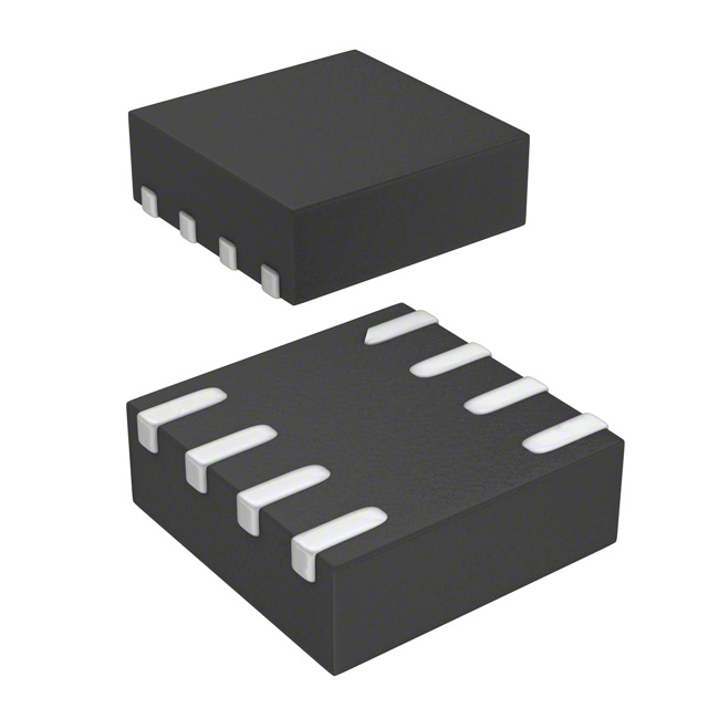


 工商网监
湘ICP备2023018690号
工商网监
湘ICP备2023018690号
