Product
Folder
Sample &
Buy
Support &
Community
Tools &
Software
Technical
Documents
DAC8311, DAC8411
SBAS439C – AUGUST 2008 – REVISED JULY 2015
DAC8x11 2-V to 5.5-V, 80-μA, 14- and 16-Bit, Low-Power, Single-Channel,
Digital-to-Analog Converters in SC70 Package
1 Features
3 Description
•
The DAC8311 (14-bit) and DAC8411 (16-bit) devices
are low-power, single-channel, voltage output digitalto-analog converters (DAC). They provide excellent
linearity and minimize undesired code-to-code
transient voltages while offering an easy upgrade
path within a pin-compatible family. All devices use a
versatile, 3-wire serial interface that operates at clock
rates of up to 50 MHz and is compatible with
standard SPI™, QSPI™, Microwire, and digital signal
processor (DSP) interfaces.
1
•
•
•
•
•
•
•
•
•
•
Relative Accuracy:
– 1 LSB INL (DAC8311: 14-bit)
– 4 LSB INL (DAC8411: 16-bit)
microPower Operation: 80 μA at 2 V
Power-Down: 0.5 μA at 5 V, 0.1 μA at 2 V
Wide Power Supply: 2 V to 5.5 V
Power-On Reset to Zero Scale
Straight Binary Data Format
Low Power Serial Interface With SchmittTriggered Inputs: Up to 50 MHz
On-Chip Output Buffer Amplifier, Rail-to-Rail
Operation
SYNC Interrupt Facility
Extended Temperature Range –40°C to 125°C
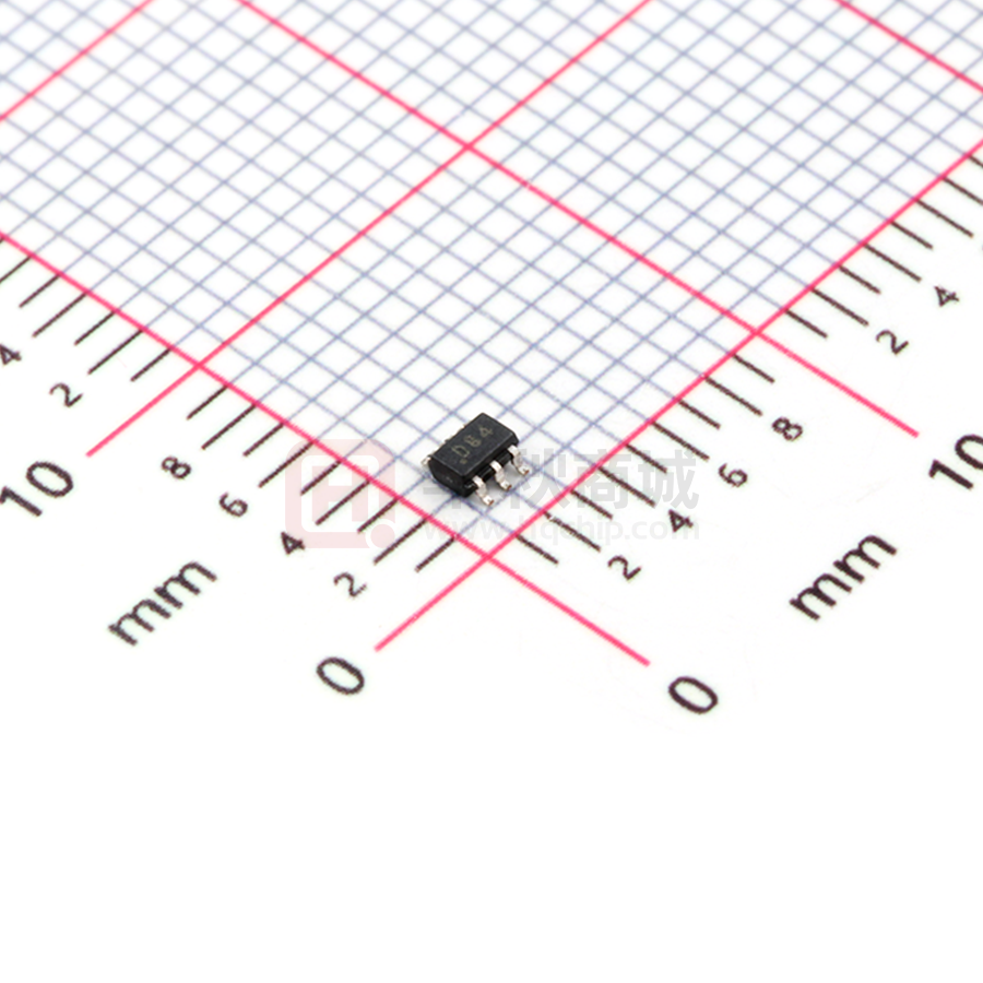
Pin-Compatible Family in a Tiny, 6-Pin SC70
Package
All devices use an external power supply as a
reference voltage to set the output range. The
devices incorporate a power-on reset (POR) circuit
that ensures the DAC output powers up at 0 V and
remains there until a valid write to the device occurs.
The DAC8311 and DAC8411 contain a power-down
feature, accessed over the serial interface, that
reduces current consumption of the device to 0.1 μA
at 2 V in power down mode. The low power
consumption of these devices in normal operation
makes it ideally suited for portable, battery-operated
equipment. The power consumption is 0.55 mW at 5
V, reducing to 2.5 μW in power-down mode.
2 Applications
•
•
•
•
Portable, Battery-Powered instruments
Process Controls
Digital Gain and Offset Adjustment
Programmable Voltage and Current Sources
These devices are pin-compatible with the DAC5311,
DAC6311, and DAC7311, offering an easy upgrade
path from 8-, 10-, and 12-bit resolution to 14- and 16bit. All devices are available in a small, 6-pin, SC70
package. This package offers a flexible, pincompatible, and functionally-compatible drop-in
solution within the family over an extended
temperature range of –40°C to 125°C.
Simplified Schematic
AVDD
GND
Power-On
Reset
Device Information(1)
PART NUMBER
REF(+)
DAC
Register
14-/16-Bit DAC
Output
Buffer
VOUT
DAC8311
DAC8411
PACKAGE
SC70 (6)
BODY SIZE (NOM)
2.00 mm × 1.25 mm
(1) For all available packages, see the orderable addendum at
the end of the data sheet.
Input Control
Logic
SYNC SCLK
Power-Down
Control Logic
Resistor
Network
DIN
1
An IMPORTANT NOTICE at the end of this data sheet addresses availability, warranty, changes, use in safety-critical applications,
intellectual property matters and other important disclaimers. PRODUCTION DATA.
�DAC8311, DAC8411
SBAS439C – AUGUST 2008 – REVISED JULY 2015
www.ti.com
Table of Contents
1
2
3
4
5
6
7
8
Features ..................................................................
Applications ...........................................................
Description .............................................................
Revision History.....................................................
Device Comparison ...............................................
Pin Configuration and Functions .........................
Specifications.........................................................
1
1
1
2
3
3
4
7.1
7.2
7.3
7.4
7.5
7.6
7.7
7.8
4
4
4
4
5
7
7
9
Absolute Maximum Ratings ......................................
ESD Ratings..............................................................
Recommended Operating Conditions.......................
Thermal Information ..................................................
Electrical Characteristics...........................................
Timing Requirements: 14-Bit ...................................
Timing Requirements: 16-Bit ....................................
Typical Characteristics ..............................................
Detailed Description ............................................ 22
8.1 Overview ................................................................. 22
8.2 Functional Block Diagram ....................................... 22
8.3 Feature Description................................................. 22
8.4 Device Functional Modes........................................ 24
8.5 Programming........................................................... 25
9
Application and Implementation ........................ 27
9.1 Application Information............................................ 27
9.2 Typical Applications ................................................ 28
10 Power Supply Recommendations ..................... 31
11 Layout................................................................... 32
11.1 Layout Guidelines ................................................. 32
11.2 Layout Example .................................................... 32
12 Device and Documentation Support ................. 33
12.1
12.2
12.3
12.4
12.5
Related Links ........................................................
Community Resources..........................................
Trademarks ...........................................................
Electrostatic Discharge Caution ............................
Glossary ................................................................
33
33
33
33
33
13 Mechanical, Packaging, and Orderable
Information ........................................................... 33
4 Revision History
NOTE: Page numbers for previous revisions may differ from page numbers in the current version.
Changes from Revision B (May 2013) to Revision C
•
Page
Added ESD Ratings table, Feature Description section, Device Functional Modes, Application and Implementation
section, Power Supply Recommendations section, Layout section, Device and Documentation Support section, and
Mechanical, Packaging, and Orderable Information section ................................................................................................. 1
Changes from Revision A (August, 2011) to Revision B
Page
•
Changed all 1.8V to 2.0V throughout data sheet ................................................................................................................... 1
•
Deleted 1.8-V Typical Characteristics section ........................................................................................................................ 9
•
Changed X-axis for Figure 35............................................................................................................................................... 13
•
Changed X-axis for Figure 36............................................................................................................................................... 13
Changes from Original (August, 2008) to Revision A
Page
•
Changed specifications and test conditions for input low voltage parameter......................................................................... 6
•
Changed specifications and test conditions for input high voltage parameter ....................................................................... 6
2
Submit Documentation Feedback
Copyright © 2008–2015, Texas Instruments Incorporated
Product Folder Links: DAC8311 DAC8411
�DAC8311, DAC8411
www.ti.com
SBAS439C – AUGUST 2008 – REVISED JULY 2015
5 Device Comparison
Table 1. Related Devices
RELATED DEVICES
16-BIT
14-BIT
12-BIT
10-BIT
8-BIT
Pin and Function
Compatible
DAC8411
DAC8311
DAC7311
DAC6311
DAC5311
Table 2. Package Information
PRODUCT
MAXIMUM RELATIVE ACCURACY (LSB)
MAXIMUM DIFFERENTIAL
NONLINEARITY (LSB)
DAC8411
±8
±2
DAC8311
±4
±1
6 Pin Configuration and Functions
DCK Package
6-Pin SC70
Top View
SYNC
1
6
VOUT
SCLK
2
5
GND
DIN
3
4
AVDD/VREF
Pin Functions
PIN
NAME
NO.
I/O
DESCRIPTION
AVDD/VREF
4
I
Power Supply Input, +2 V to +5.5 V.
DIN
3
I
Serial Data Input. Data is clocked into the 24-bit (DAC8411) or 16-bit (DAC8311) input shift
register on the falling edge of the serial clock input.
GND
5
—
SCLK
2
I
Serial Clock Input. Data can be transferred at rates up to 50 MHz.
Ground reference point for all circuitry on the part.
SYNC
1
I
Level-triggered control input (active low). This is the frame sychronization signal for the input
data. When SYNC goes low, it enables the input shift register and data are transferred in on the
falling edges of the following clocks. The DAC is updated following the 24th (DAC8411) or 16th
(DAC8311) clock cycle, unless SYNC is taken high before this edge, in which case the rising
edge of SYNC acts as an interrupt and the write sequence is ignored by the DAC8x11. Refer to
the DAC8311 and DAC8411 SYNC Interrupt sections for more details.
VOUT
6
O
Analog output voltage from DAC. The output amplifier has rail-to-rail operation.
Copyright © 2008–2015, Texas Instruments Incorporated
Product Folder Links: DAC8311 DAC8411
Submit Documentation Feedback
3
�DAC8311, DAC8411
SBAS439C – AUGUST 2008 – REVISED JULY 2015
www.ti.com
7 Specifications
7.1 Absolute Maximum Ratings
over operating free-air temperature range (unless otherwise noted) (1)
Voltage
Temperature
(1)
MIN
MAX
UNIT
AVDD to GND
–0.3
6
V
Digital input voltage to GND
–0.3
AVDD +0.3
V
VOUT to GND
–0.3
AVDD +0.3
V
150
°C
150
°C
Junction, TJ max
Storage, Tstg
–65
Stresses beyond those listed under Absolute Maximum Ratings may cause permanent damage to the device. These are stress ratings
only, which do not imply functional operation of the device at these or any other conditions beyond those indicated under Recommended
Operating Conditions. Exposure to absolute-maximum-rated conditions for extended periods may affect device reliability.
7.2 ESD Ratings
VALUE
Human-body model (HBM), per ANSI/ESDA/JEDEC JS-001
V(ESD)
(1)
(2)
Electrostatic discharge
(1)
UNIT
±1000
Charged-device model (CDM), per JEDEC specification JESD22C101 (2)
±500
V
JEDEC document JEP155 states that 500-V HBM allows safe manufacturing with a standard ESD control process.
JEDEC document JEP157 states that 250-V CDM allows safe manufacturing with a standard ESD control process.
7.3 Recommended Operating Conditions
over operating free-air temperature range (unless otherwise noted)
MIN
NOM
MAX
UNIT
TA
Operating temperature
–40
+125
°C
AVDD
Supply voltage
2.0
+5.5
V
7.4 Thermal Information
DAC8x11
THERMAL METRIC (1)
DCK (SC70)
UNIT
6 PINS
RθJA
Junction-to-ambient thermal resistance
216.4
°C/W
RθJC(top)
Junction-to-case (top) thermal resistance
52.1
°C/W
RθJB
Junction-to-board thermal resistance
65.9
°C/W
ψJT
Junction-to-top characterization parameter
1.3
°C/W
ψJB
Junction-to-board characterization parameter
65.2
°C/W
RθJC(bot)
Junction-to-case (bottom) thermal resistance
N/A
°C/W
(1)
4
For more information about traditional and new thermal metrics, see the Semiconductor and IC Package Thermal Metrics application
report, SPRA953.
Submit Documentation Feedback
Copyright © 2008–2015, Texas Instruments Incorporated
Product Folder Links: DAC8311 DAC8411
�DAC8311, DAC8411
www.ti.com
SBAS439C – AUGUST 2008 – REVISED JULY 2015
7.5 Electrical Characteristics
at AVDD = 2 V to 5.5 V, RL = 2 kΩ to GND, and CL = 200 pF to GND, and TA = –40°C to +125°C unless otherwise noted.
PARAMETER
DAC8411, DAC8311
TEST CONDITIONS
MIN
TYP
MAX
±4
±8
±4
±12
±0.5
±2
UNIT
STATIC PERFORMANCE (1)
Resolution
DAC8411
Relative accuracy
16
3.6 V to 5 V
Measured by the line passing
through codes 485 and 64714 2 V to 3.6 V
Differential
nonlinearity
Resolution
DAC8311
Differential
nonlinearity
Measured by the line passing through two codes
(2)
Offset error drift
LSB
Bits
±1
±4
LSB
±0.125
±1
LSB
±0.05
±4
All zeros loaded to the DAC register
Full-scale error
All ones loaded to DAC register
mV
μV/°C
3
Zero code error
0.2
Gain error
Gain temperature coefficient
LSB
14
Measured by the line passing through codes 120 and
Relative accuracy
16200
Offset error
Bits
mV
0.04
0.2
% of FSR
0.05
±0.15
% of FSR
AVDD = 5 V
±0.5
AVDD = 2 V
±1.5
ppm of
FSR/°C
OUTPUT CHARACTERISTICS
Output voltage range
Output voltage settling time (3)
0
RL = 2 kΩ, CL = 200 pF, AVDD = 5 V,
1/4 scale to 3/4 scale
RL = 2 MΩ, CL = 470 pF
Slew rate
Capacitive load stability
Code change glitch impulse
RL = ∞
RL = 2 kΩ
1LSB change around major carry
Power-up time
10
μs
12
μs
0.7
V/μs
470
pF
pF
0.5
nV-s
0.5
nV-s
17
mV
0.5
Ω
AVDD = 5 V
50
mA
AVDD = 3 V
20
mA
Coming out of power-down mode
50
μs
RL = 2 kΩ, CL = 200 pF, AVDD = 5 V
DC output impedance
Short-circuit current
V
1000
Digital feedthrough
Power-on glitch impulse
6
AVDD
AC PERFORMANCE
SNR
THD
SFDR
TA= 25°C, BW = 20 kHz, 16-bit level, AVDD = 5 V,
fOUT = 1 kHz, 1st 19 harmonics removed for SNR
calculation
SINAD
DAC output noise density (4)
DAC output noise (5)
(1)
(2)
(3)
(4)
(5)
88
dB
–66
dB
66
dB
66
dB
TA= 25°C, at zero-scale input,
fOUT = 1 kHz, AVDD = 5 V
17
nV/√Hz
TA= 25°C, at mid-code input,
fOUT = 1 kHz, AVDD = 5 V
110
nV/√Hz
TA= 25°C, at mid-code input,
0.1 Hz to 10 Hz, AVDD = 5 V
3
μVpp
Linearity calculated using a reduced code range of 485 to 64714 for 16-bit, and 120 to 16200 for 14-bit, output unloaded.
Straight line passing through codes 485 and 64714 for 16-bit, and 120 and 16200 for 14-bit, output unloaded.
Specified by design and characterization, not production tested.
For more details, see Figure 33.
For more details, see Figure 34.
Copyright © 2008–2015, Texas Instruments Incorporated
Product Folder Links: DAC8311 DAC8411
Submit Documentation Feedback
5
�DAC8311, DAC8411
SBAS439C – AUGUST 2008 – REVISED JULY 2015
www.ti.com
Electrical Characteristics (continued)
at AVDD = 2 V to 5.5 V, RL = 2 kΩ to GND, and CL = 200 pF to GND, and TA = –40°C to +125°C unless otherwise noted.
PARAMETER
DAC8411, DAC8311
TEST CONDITIONS
MIN
TYP
MAX
UNIT
LOGIC INPUTS (3)
±1
μA
AVDD = 2.7 V to 5.5 V
0.3 × AVDD
V
AVDD = 2 V to 2.7 V
0.1 × AVDD
V
Input current
VINL, input low voltage
VINH, input high voltage
AVDD = 2.7 V to 5.5 V
0.7 × AVDD
V
AVDD = 2 V to 2.7 V
0.9 × AVDD
V
Pin capacitance
1.5
3
pF
5.5
V
POWER REQUIREMENTS
AVDD
2
Normal mode
VINH = AVDD and VINL =
GND, at mid-scale code (6)
IDD
All power-down
mode
Normal mode
VINH = AVDD and VINL =
GND, at mid-scale code (6)
VINH = AVDD and VINL =
GND, at mid-scale code (6)
Power
dissipation
All power-down
mode
(6)
6
VINH = AVDD and VINL =
GND, at mid-scale code (6)
AVDD = 3.6 V to 5.5 V
110
160
AVDD = 2.7 V to 3.6 V
95
150
AVDD = 2 V to 2.7 V
80
140
AVDD = 3.6 V to 5.5 V
0.5
3.5
AVDD = 2.7 V to 3.6 V
0.4
3.0
AVDD = 2 V to 2.7 V
0.1
2.0
AVDD = 3.6 V to 5.5 V
0.55
0.88
AVDD = 2.7 V to 3.6 V
0.25
0.54
AVDD = 2 V to 2.7 V
0.14
0.38
AVDD = 3.6 V to 5.5 V
2.50
19.2
AVDD = 2.7 V to 3.6 V
1.08
10.8
AVDD = 2 V to 2.7 V
0.72
8.1
μA
μA
mW
μW
For more details, see Figure 14 and Figure 55.
Submit Documentation Feedback
Copyright © 2008–2015, Texas Instruments Incorporated
Product Folder Links: DAC8311 DAC8411
�DAC8311, DAC8411
www.ti.com
SBAS439C – AUGUST 2008 – REVISED JULY 2015
7.6 Timing Requirements: 14-Bit
All specifications at –40°C to 125°C, and AVDD = 2 V to 5.5 V, unless otherwise noted. (1)
PARAMETER
TEST CONDITIONS
f(SCLK)
Serial clock frequency
t1
SCLK cycle time
t2
SCLK high time
t3
SCLK low time
t4
SYNC to SCLK rising edge setup time
t5
Data setup time
t6
Data hold time
t7
SCLK falling edge to SYNC rising edge
t8
Minimum SYNC high time
t9
16th SCLK falling edge to SYNC falling edge
t10
SYNC rising edge to 16th SCLK falling edge
(for successful SYNC interrupt)
(1)
(2)
(2)
MIN
TYP
MAX
AVDD = 2.0 V to 3.6 V
20
AVDD = 3.6 V to 5.5 V
50
AVDD = 2 V to 3.6 V
50
AVDD = 3.6 V to 5.5 V
20
AVDD = 2 V to 3.6 V
25
AVDD = 3.6 V to 5.5 V
10
AVDD = 2 V to 3.6 V
25
AVDD = 3.6 V to 5.5 V
10
AVDD = 2 V to 3.6 V
0
AVDD = 3.6 V to 5.5 V
0
AVDD = 2 V to 3.6 V
5
AVDD = 3.6 V to 5.5 V
5
AVDD = 2 V to 3.6 V
4.5
AVDD = 3.6 V to 5.5 V
4.5
AVDD = 2 V to 3.6 V
0
AVDD = 3.6 V to 5.5 V
0
AVDD = 2 V to 3.6 V
50
AVDD = 3.6 V to 5.5 V
20
AVDD = 2 V to 3.6 V
100
AVDD = 3.6 V to 5.5 V
100
AVDD = 2 V to 3.6 V
15
AVDD = 3.6 V to 5.5 V
15
UNIT
MHz
ns
ns
ns
ns
ns
ns
ns
ns
ns
ns
All input signals are specified with tR = tF = 3 ns (10% to 90% of AVDD) and timed from a voltage level of (VIL + VIH)/2.
See Figure 1 timing diagram.
7.7 Timing Requirements: 16-Bit
All specifications at –40°C to 125°C, and AVDD = 2 V to 5.5 V, unless otherwise noted. (1)
PARAMETER
TEST CONDITIONS
f(SCLK)
Serial clock frequency
t1
SCLK cycle time
t2
SCLK high time
t3
SCLK low time
t4
SYNC to SCLK rising edge setup time
t5
Data setup time
t6
Data hold time
t7
SCLK falling edge to SYNC rising edge
(1)
(2)
(2)
MIN
TYP
MAX
AVDD = 2.0 V to 3.6 V
20
AVDD = 3.6 V to 5.5 V
50
AVDD = 2 V to 3.6 V
50
AVDD = 3.6 V to 5.5 V
20
AVDD = 2 V to 3.6 V
25
AVDD = 3.6 V to 5.5 V
10
AVDD = 2 V to 3.6 V
25
AVDD = 3.6 V to 5.5 V
10
AVDD = 2 V to 3.6 V
0
AVDD = 3.6 V to 5.5 V
0
AVDD = 2 V to 3.6 V
5
AVDD = 3.6 V to 5.5 V
5
AVDD = 2 V to 3.6 V
4.5
AVDD = 3.6 V to 5.5 V
4.5
AVDD = 2 V to 3.6 V
0
AVDD = 3.6 V to 5.5 V
0
UNIT
MHz
ns
ns
ns
ns
ns
ns
ns
All input signals are specified with tR = tF = 3 ns (10% to 90% of AVDD) and timed from a voltage level of (VIL + VIH)/2.
See Figure 2 timing diagram.
Copyright © 2008–2015, Texas Instruments Incorporated
Product Folder Links: DAC8311 DAC8411
Submit Documentation Feedback
7
�DAC8311, DAC8411
SBAS439C – AUGUST 2008 – REVISED JULY 2015
www.ti.com
Timing Requirements: 16-Bit (continued)
All specifications at –40°C to 125°C, and AVDD = 2 V to 5.5 V, unless otherwise noted.(1) (2)
PARAMETER
TEST CONDITIONS
t8
Minimum SYNC high time
t9
24th SCLK falling edge to SYNC falling edge
t10
SYNC rising edge to 24th SCLK falling edge
(for successful SYNC interrupt)
AVDD = 2 V to 3.6 V
50
AVDD = 3.6 V to 5.5 V
20
AVDD = 2 V to 3.6 V
100
AVDD = 3.6 V to 5.5 V
100
AVDD = 2 V to 3.6 V
15
AVDD = 3.6 V to 5.5 V
15
TYP
MAX
UNIT
ns
ns
ns
t9
t1
SCLK
MIN
1
16
t8
t2
t3
t4
t7
SYNC
t10
t6
t5
DB15
DIN
DB0
DB15
Figure 1. Serial Write Operation: 14-Bit (DAC8311)
t9
t1
SCLK
1
24
t8
t3
t4
t2
t7
SYNC
t6
t10
t5
DIN
DB23
DB0
DB23
Figure 2. Serial Write Operation: 16-Bit (DAC8411)
8
Submit Documentation Feedback
Copyright © 2008–2015, Texas Instruments Incorporated
Product Folder Links: DAC8311 DAC8411
�DAC8311, DAC8411
www.ti.com
SBAS439C – AUGUST 2008 – REVISED JULY 2015
7.8 Typical Characteristics
7.8.1 Typical Characteristics: AVDD = 5 V
at TA = 25°C, AVDD = 5 V, and DAC loaded with mid-scale code, unless otherwise noted.
2
AVDD = 5V
0
-1
-2
0.2
0.5
DLE (LSB)
DLE (LSB)
1.0
0
-0.5
-1.0
0
8192
16384 24576 32768 40960 49152
0.1
0
-0.1
-0.2
57344 65536
0
4096
6144
8192
10240 12288
14336 16384
Digital Input Code
Figure 3. DAC8411 16-Bit Linearity Error and Differential
Linearity Error vs Code (–40°C)
Figure 4. DAC8311 14-Bit Linearity Error and Differential
Linearity Error vs Code (–40°C)
2
AVDD = 5V
0
-1
-2
0.2
0.5
DLE (LSB)
DLE (LSB)
AVDD = 5V
1
LE (LSB)
LE (LSB)
6
4
2
0
-2
-4
-6
0
-0.5
-1.0
0
8192
16384 24576 32768 40960 49152
0.1
0
-0.1
-0.2
57344 65536
0
2048
4096
6144
8192
10240 12288
14336 16384
Digital Input Code
Digital Input Code
Figure 5. DAC8411 16-Bit Linearity Error and Differential
Linearity Error vs Code (25°C)
Figure 6. DAC8311 14-Bit Linearity Error and Differential
Linearity Error vs Code (25°C)
6
4
2
0
-2
-4
-6
2
AVDD = 5V
LE (LSB)
LE (LSB)
2048
Digital Input Code
1.0
AVDD = 5V
1
0
-1
-2
1.0
0.2
0.5
DLE (LSB)
DLE (LSB)
AVDD = 5V
1
LE (LSB)
LE (LSB)
6
4
2
0
-2
-4
-6
0
-0.5
-1.0
0
8192
16384 24576 32768 40960 49152
57344 65536
0.1
0
-0.1
-0.2
0
2048
4096
6144
8192
10240 12288
14336 16384
Digital Input Code
Digital Input Code
Figure 7. DAC8411 16-Bit Linearity Error and Differential
Linearity Error vs Code (125°C)
Figure 8. DAC8311 14-Bit Linearity Error and Differential
Linearity Error vs Code (125°C)
Copyright © 2008–2015, Texas Instruments Incorporated
Product Folder Links: DAC8311 DAC8411
Submit Documentation Feedback
9
�DAC8311, DAC8411
SBAS439C – AUGUST 2008 – REVISED JULY 2015
www.ti.com
Typical Characteristics: AVDD = 5 V (continued)
at TA = 25°C, AVDD = 5 V, and DAC loaded with mid-scale code, unless otherwise noted.
0.4
5.5
Analog Output Voltage (V)
Zero-Code Error (mV)
AVDD = 5V
0.3
0.2
0.1
0
-40 -25 -10
5.0
4.5
4.0
3.5
3.0
AVDD = 5V
DAC Loaded with FFFFh
2.5
5
20
35
50
65
80
95
110 125
0
2
Temperature (°C)
10
0.6
AVDD = 5V
DAC Loaded with 0000h
AVDD = 5V
Analog Output Voltage (V)
0.4
Offset Error (mV)
8
Figure 10. Source Current at Positive Rail
0.6
0.2
0
-0.2
-0.4
-0.6
-40 -25 -10
0.4
0.2
0
5
20
35
50
65
80
95
110 125
0
2
Temperature (°C)
4
6
8
10
ISINK (mA)
Figure 11. Offset Error vs Temperature
Figure 12. Sink Current at Negative Rail
120
0.06
AVDD = 5.5V
AVDD = 5V
Power-Supply Current (mA)
0.04
Full-Scale Error (mV)
6
ISOURCE (mA)
Figure 9. Zero-Code Error vs Temperature
0.02
0
-0.02
-0.04
-0.06
-40 -25 -10
100
80
60
5
20
35
50
65
80
95
110 125
0
8192 16384 24576 32768 40960 49152 57344 65536
Digital Input Code
Temperature (°C)
Figure 13. Full-Scale Error vs Temperature
10
4
Submit Documentation Feedback
Figure 14. Power-Supply Current vs Digital Input Code
Copyright © 2008–2015, Texas Instruments Incorporated
Product Folder Links: DAC8311 DAC8411
�DAC8311, DAC8411
www.ti.com
SBAS439C – AUGUST 2008 – REVISED JULY 2015
Typical Characteristics: AVDD = 5 V (continued)
at TA = 25°C, AVDD = 5 V, and DAC loaded with mid-scale code, unless otherwise noted.
140
1.6
AVDD = 5V
Quiescent Current (mA)
Power-Supply Current (mA)
AVDD = 5V
130
120
110
100
-40 -25 -10
5
20
35
50
65
80
95
1.2
0.8
0.4
0
-40 -25 -10
110 125
5
20
Temperature (°C)
Figure 15. Power-Supply Current vs Temperature
50
65
80
95
110 125
Figure 16. Power-Down Current vs Temperature
50
2000
SYNC Input (all other digital inputs = GND)
AVDD = 5.5V
45
40
1500
35
Sweep from
0V to 5.5V
Occurrences
Power-Supply Current (mA)
35
Temperature (°C)
1000
Sweep from
5.5V to 0V
30
25
20
15
500
10
5
-50
136
140
128
Figure 18. Power-Supply Current Histogram
Figure 17. Power-Supply Current vs Logic Input Voltage
94
AVDD = 5V, fS = 225kSPS,
-1dB FSR Digital Input,
Measurement Bandwidth = 20kHz
132
IDD (mA)
VLOGIC (V)
-40
120
5.0
124
4.5
112
4.0
116
3.5
104
3.0
108
2.5
96
2.0
100
1.5
88
1.0
92
0.5
80
0
84
0
0
AVDD = 5V,
fS = 225kSPS,
-1dB FSR Digital Input,
Measurement Bandwidth = 20kHz
THD
92
SNR (dB)
THD (dB)
-60
2nd Harmonic
-70
90
88
-80
3rd Harmonic
86
-90
84
-100
0
1
2
3
4
5
0
fOUT (kHz)
1
2
3
4
5
fOUT (kHz)
Figure 19. Total Harmonic Distortion vs Output Frequency
Figure 20. Signal-to-Noise Ratio vs Output Frequency
Copyright © 2008–2015, Texas Instruments Incorporated
Product Folder Links: DAC8311 DAC8411
Submit Documentation Feedback
11
�DAC8311, DAC8411
SBAS439C – AUGUST 2008 – REVISED JULY 2015
www.ti.com
Typical Characteristics: AVDD = 5 V (continued)
at TA = 25°C, AVDD = 5 V, and DAC loaded with mid-scale code, unless otherwise noted.
0
AVDD = 5V,
fOUT = 1kHz, fS = 225kSPS,
Measurement Bandwidth = 20kHz
VOUT (500mV/div)
20
Gain (dB)
-40
-60
-80
-100
AVDD = 5V
Clock Feedthrough Impulse ~0.5nV-s
-120
-140
0
5
10
15
Time (500ns/div)
20
Frequency (kHz)
Figure 22. Clock Feedthrough 5 V, 2 mHz, Midscale
VOUT (100mV/div)
AVDD = 5V
From Code: 7FFFh
To Code: 8000h
Clock
Feedthrough
~0.5nV-s
AVDD = 5V
From Code: 8000h
To Code: 7FFFh
VOUT (100mV/div)
Figure 21. Power Spectral Density
Clock
Feedthrough
~0.5nV-s
Glitch Impulse
< 0.5nV-s
Time (5ms/div)
Time (5ms/div)
Glitch Impulse
< 0.5nV-s
AVDD = 5V
From Code: 2000h
To Code: 2001h
Figure 24. Glitch Energy 5 V, 16-Bit, 1LSB Step, Falling
Edge
VOUT (100mV/div)
VOUT (100mV/div)
Figure 23. Glitch Energy 5 V, 16-Bit, 1LSB Step, Rising
Edge
Clock
Feedthrough
~0.5nV-s
AVDD = 5V
From Code: 2001h
To Code: 2000h
Clock
Feedthrough
~0.5nV-s
Glitch Impulse
< 0.5nV-s
Time (5ms/div)
Time (5ms/div)
Figure 25. Glitch Energy 5 V, 14-Bit, 1LSB Step, Rising
Edge
12
Submit Documentation Feedback
Glitch Impulse
< 0.5nV-s
Figure 26. Glitch Energy 5 V, 14-Bit, 1LSB Step, Falling
Edge
Copyright © 2008–2015, Texas Instruments Incorporated
Product Folder Links: DAC8311 DAC8411
�DAC8311, DAC8411
www.ti.com
SBAS439C – AUGUST 2008 – REVISED JULY 2015
Typical Characteristics: AVDD = 5 V (continued)
at TA = 25°C, AVDD = 5 V, and DAC loaded with mid-scale code, unless otherwise noted.
AVDD = 5V
From Code: 0000h
To Code: FFFFh
AVDD = 5V
From Code: FFFFh
To Code: 0000h
Rising Edge
1V/div
Zoomed Rising Edge
100mV/div
Falling Edge
1V/div
Zoomed Falling Edge
100mV/div
Trigger Pulse 5V/div
Trigger Pulse 5V/div
Time (2ms/div)
Time (2ms/div)
Figure 27. Full-Scale Settling Time 5-V Rising Edge
Figure 28. Full-Scale Settling Time 5-V Falling Edge
AVDD = 5V
From Code: C000h
To Code: 4000h
Falling
Edge
1V/div
Rising
Edge
1V/div
Zoomed Falling Edge
100mV/div
Zoomed Rising Edge
100mV/div
AVDD = 5V
From Code: 4000h
To Code: C000h
Trigger
Pulse
5V/div
Trigger
Pulse
5V/div
Time (2ms/div)
Time (2ms/div)
17mV
AVDD (2V/div)
AVDD = 5V
DAC = Zero Scale
Load = 200pF || 10kW
Figure 30. Half-Scale Settling Time 5-V Falling Edge
AVDD = 5V
DAC = Zero Scale
Load = 200pF || 10kW
VOUT (20mV/div)
VOUT (20mV/div)
AVDD (2V/div)
Figure 29. Half-Scale Settling Time 5-V Rising Edge
Time (5ms/div)
Time (10ms/div)
Figure 31. Power-On Reset to 0 V Power-On Glitch
Copyright © 2008–2015, Texas Instruments Incorporated
Product Folder Links: DAC8311 DAC8411
Figure 32. Power-Off Glitch
Submit Documentation Feedback
13
�DAC8311, DAC8411
SBAS439C – AUGUST 2008 – REVISED JULY 2015
www.ti.com
Typical Characteristics: AVDD = 5 V (continued)
at TA = 25°C, AVDD = 5 V, and DAC loaded with mid-scale code, unless otherwise noted.
300
AVDD = 5V,
DAC = Midscale, No Load
AVDD = 5V
VNOISE (1mV/div)
Noise (nV/ÖHz)
250
200
150
Midscale
100
3mVPP
Zero Scale
Full Scale
50
0
10
100
1k
10k
Time (2s/div)
100k
Frequency (Hz)
Figure 34. DAC Output Noise 0.1 Hz to 10 Hz Bandwidth
Figure 33. DAC Output Noise Density vs Frequency
120
0.4
AVDD = 2.0V to 5.5V
110
Quiescent Current (mA)
Power-Supply Current (mA)
AVDD = 2.0V to 5.5V
100
90
80
70
0.3
0.2
0.1
0
2.0
2.5
3.0
3.5
4.0
4.5
5.0
5.5
2.0
2.5
Figure 35. Power-Supply Current vs Power-Supply Voltage
14
Submit Documentation Feedback
3.0
3.5
4.0
4.5
5.0
5.5
AVDD (V)
AVDD (V)
Figure 36. Power-Down Current vs Power-Supply Voltage
Copyright © 2008–2015, Texas Instruments Incorporated
Product Folder Links: DAC8311 DAC8411
�DAC8311, DAC8411
www.ti.com
SBAS439C – AUGUST 2008 – REVISED JULY 2015
7.8.2 Typical Characteristics: AVDD = 3.6 V
at TA = 25°C, and AVDD = 3.6 V, unless otherwise noted.
100
140
AVDD = 3.6V
Power-Supply Current (mA)
Power-Supply Current (mA)
AVDD = 3.6V
90
80
70
60
50
0
130
120
110
100
90
80
-40 -25 -10
8192 16384 24576 32768 40960 49152 57344 65536
35
50
65
80
95
110 125
Figure 37. Power-Supply Current vs Digital Input Code
Figure 38. Power-Supply Current vs Temperature
1.2
SYNC Input (all other digital inputs = GND)
AVDD = 3.6V
Quiescent Current (mA)
Power-Supply Current (mA)
20
Temperature (°C)
1200
900
Sweep from
0V to 3.6V
600
300
0.8
0.4
Sweep from
3.6V to 0V
0
0
0.5
1.0
1.5
2.0
2.5
3.0
3.5
0
-40 -25 -10
4.0
VLOGIC (V)
5
20
35
50
65
80
95
110 125
Temperature (°C)
Figure 39. Power-Supply Current vs Logic Input Voltage
Figure 40. Power-Down Current vs Temperature
3.7
0.6
AVDD = 3.6V
DAC Loaded with 0000h
3.5
Analog Output Voltage (V)
Analog Output Voltage (V)
5
Digital Input Code
3.3
3.1
2.9
2.7
AVDD = 3.6V
DAC Loaded with FFFFh
2.5
0
2
4
0.4
0.2
0
6
8
10
0
2
ISOURCE (mA)
4
6
8
10
ISINK (mA)
Figure 41. Source Current at Positive Rail
Figure 42. Sink Current at Negative Rail
Copyright © 2008–2015, Texas Instruments Incorporated
Product Folder Links: DAC8311 DAC8411
Submit Documentation Feedback
15
�DAC8311, DAC8411
SBAS439C – AUGUST 2008 – REVISED JULY 2015
www.ti.com
Typical Characteristics: AVDD = 3.6 V (continued)
at TA = 25°C, and AVDD = 3.6 V, unless otherwise noted.
50
45
AVDD = 3.6V
40
Occurrences
35
30
25
20
15
10
5
126
130
118
122
110
114
102
106
94
98
86
90
78
82
70
74
0
IDD (mA)
Figure 43. Power-Supply Current Histogram
7.8.3 Typical Characteristics: AVDD = 2.7 V
6
4
2
0
-2
-4
-6
2
AVDD = 2.7V
LE (LSB)
LE (LSB)
at TA = 25°C, and AVDD = 2.7 V, unless otherwise noted.
-2
0.2
DLE (LSB)
DLE (LSB)
0
-1
1.0
0.5
0
-0.5
0.1
0
-0.1
-0.2
-1.0
0
16
AVDD = 2.7V
1
8192
16384 24576 32768 40960 49152
57344 65536
0
2048
4096
6144
8192
10240 12288
14336 16384
Digital Input Code
Digital Input Code
Figure 44. DAC8411 16-Bit Linearity Error and Differential
Linearity Error vs Code (–40°C)
Figure 45. DAC8311 14-Bit Linearity Error and Differential
Linearity Error vs Code (–40°C)
Submit Documentation Feedback
Copyright © 2008–2015, Texas Instruments Incorporated
Product Folder Links: DAC8311 DAC8411
�DAC8311, DAC8411
www.ti.com
SBAS439C – AUGUST 2008 – REVISED JULY 2015
Typical Characteristics: AVDD = 2.7 V (continued)
6
4
2
0
-2
-4
-6
2
AVDD = 2.7V
LE (LSB)
LE (LSB)
at TA = 25°C, and AVDD = 2.7 V, unless otherwise noted.
-2
0.2
DLE (LSB)
DLE (LSB)
0.5
0
-0.5
0.1
0
-0.1
-0.2
-1.0
0
8192
16384 24576 32768 40960 49152
0
57344 65536
2048
4096
6144
8192
10240 12288
14336 16384
Digital Input Code
Digital Input Code
Figure 46. DAC8411 16-Bit Linearity Error and Differential
Linearity Error vs Code (25°C)
Figure 47. DAC8311 14-Bit Linearity Error and Differential
Linearity Error vs Code (25°C)
6
4
2
0
-2
-4
-6
2
AVDD = 2.7V
LE (LSB)
LE (LSB)
0
-1
1.0
AVDD = 2.7V
1
0
-1
-2
0.2
DLE (LSB)
1.0
DLE (LSB)
AVDD = 2.7V
1
0.5
0
-0.5
0.1
0
-0.1
-0.2
-1.0
0
8192
16384 24576 32768 40960 49152
0
57344 65536
2048
4096
6144
8192
10240 12288
14336 16384
Digital Input Code
Digital Input Code
Figure 48. DAC8411 16-Bit Linearity Error and Differential
Linearity Error vs Code (125°C)
Figure 49. DAC8311 14-Bit Linearity Error and Differential
Linearity Error vs Code (125°C)
0.4
2.8
Analog Output Voltage (V)
Zero-Code Error (mV)
AVDD = 2.7V
0.3
0.2
0.1
0
-40 -25 -10
2.6
2.4
2.2
AVDD = 2.7V
DAC Loaded with FFFFh
2.0
5
20
35
50
65
80
95
110 125
0
2
Temperature (°C)
4
6
8
10
ISOURCE (mA)
Figure 50. Zero-Code Error vs Temperature
Figure 51. Source Current at Positive Rail
Copyright © 2008–2015, Texas Instruments Incorporated
Product Folder Links: DAC8311 DAC8411
Submit Documentation Feedback
17
�DAC8311, DAC8411
SBAS439C – AUGUST 2008 – REVISED JULY 2015
www.ti.com
Typical Characteristics: AVDD = 2.7 V (continued)
at TA = 25°C, and AVDD = 2.7 V, unless otherwise noted.
0.6
0.6
AVDD = 2.7V
DAC Loaded with 0000h
AVDD = 2.7V
Analog Output Voltage (V)
Offset Error (mV)
0.4
0.2
0
-0.2
-0.4
-0.6
-40 -25 -10
0.4
0.2
0
5
20
35
50
65
80
95
110 125
0
2
4
Temperature (°C)
Figure 52. Offset Error vs Temperature
AVDD = 2.7V
Power-Supply Current (mA)
0.04
Full-Scale Error (mV)
10
100
AVDD = 2.7V
0.02
0
-0.02
-0.04
-0.06
-40 -25 -10
90
80
70
60
50
5
20
35
50
65
80
95
0
110 125
8192 16384 24576 32768 40960 49152 57344 65536
Digital Input Code
Temperature (°C)
Figure 54. Full-Scale Error vs Temperature
Figure 55. Power-Supply Current vs Digital Input Code
120
1.0
AVDD = 2.7V
AVDD = 2.7V
110
Quiescent Current (mA)
Power-Supply Current (mA)
8
Figure 53. Sink Current at Negative Rail
0.06
100
90
80
70
-40 -25 -10
5
20
35
50
65
80
95
110 125
0.8
0.6
0.4
0.2
0
-40 -25 -10
Temperature (°C)
Submit Documentation Feedback
5
20
35
50
65
80
95
110 125
Temperature (°C)
Figure 56. Power-Supply Current vs Temperature
18
6
ISINK (mA)
Figure 57. Power-Down Current vs Temperature
Copyright © 2008–2015, Texas Instruments Incorporated
Product Folder Links: DAC8311 DAC8411
�DAC8311, DAC8411
www.ti.com
SBAS439C – AUGUST 2008 – REVISED JULY 2015
Typical Characteristics: AVDD = 2.7 V (continued)
at TA = 25°C, and AVDD = 2.7 V, unless otherwise noted.
50
800
AVDD = 2.7V
45
40
600
35
Occurrences
Power-Supply Current (mA)
SYNC Input (all other digital inputs = GND)
Sweep from
0V to 2.7V
400
Sweep from
2.7V to 0V
30
25
20
15
200
10
5
VLOGIC (V)
104
96
100
92
IDD (mA)
Figure 58. Power-Supply Current vs Logic Input Voltage
Figure 59. Power-Supply Current Histogram
88
-20
AVDD = 2.7V, fS = 225kSPS,
-1dB FSR Digital Input,
Measurement Bandwidth = 20kHz
AVDD = 2.7V, fS = 225kSPS,
-1dB FSR Digital Input,
Measurement Bandwidth = 20kHz
86
THD
SNR (dB)
-40
THD (dB)
88
3.0
84
2.5
76
2.0
80
1.5
72
1.0
68
0.5
60
0
64
0
0
-60
84
2nd Harmonic
82
-80
3rd Harmonic
80
-100
0
1
2
3
4
5
0
fOUT (kHz)
1
2
3
4
5
fOUT (kHz)
Figure 60. Total Harmonic Distortion vs Output Frequency
Figure 61. Signal-to-Noise Ratio vs Output Frequency
0
AVDD = 2.7V,
fOUT = 1kHz, fS = 225kSPS,
Measurement Bandwidth = 20kHz
VOUT (500mV/div)
20
Gain (dB)
-40
-60
-80
-100
AVDD = 2.7V
Clock Feedthrough Impulse ~0.4nV-s
-120
-140
0
5
10
15
Time (5ms/div)
20
Frequency (kHz)
Figure 62. Power Spectral Density
Figure 63. Clock Feedthrough 2.7 V, 20 mHz, Midscale
Copyright © 2008–2015, Texas Instruments Incorporated
Product Folder Links: DAC8311 DAC8411
Submit Documentation Feedback
19
�DAC8311, DAC8411
SBAS439C – AUGUST 2008 – REVISED JULY 2015
www.ti.com
Typical Characteristics: AVDD = 2.7 V (continued)
at TA = 25°C, and AVDD = 2.7 V, unless otherwise noted.
AVDD = 2.7V
From Code: 8000h
To Code: 7FFFh
Glitch Impulse
< 0.3nV-s
Clock
Feedthrough
~0.4nV-s
VOUT (100mV/div)
VOUT (100mV/div)
AVDD = 2.7V
From Code: 7FFFh
To Code: 8000h
Glitch Impulse
< 0.3nV-s
Clock
Feedthrough
~0.4nV-s
Time (5ms/div)
Time (5ms/div)
Figure 64. Glitch Energy 2.7 V, 16-Bit, 1LSB Step, Rising
Edge
Figure 65. Glitch Energy 2.7 V, 16-Bit, 1LSB Step, Falling
Edge
AVDD = 2.7V
From Code: 2001h
To Code: 2000h
Glitch Impulse
< 0.3nV-s
Clock
Feedthrough
~0.4nV-s
VOUT (100mV/div)
VOUT (100mV/div)
AVDD = 2.7V
From Code: 2000h
To Code: 2001h
Clock
Feedthrough
~0.4nV-s
Time (5ms/div)
Glitch Impulse
< 0.3nV-s
Time (5ms/div)
Figure 66. Glitch Energy 2.7 V, 14-Bit, 1LSB Step, Rising
Edge
Figure 67. Glitch Energy 2.7 V, 14-Bit, 1LSB Step, Falling
Edge
AVDD = 2.7V
From Code: 0000h
To Code: FFFFh
AVDD = 2.7V
From Code: FFFFh
To Code: 0000h
Falling Edge
1V/div
Rising Edge
1V/div
Zoomed Rising Edge
100mV/div
Trigger
Pulse
2.7V/div
Zoomed Falling Edge
100mV/div
Trigger Pulse 2.7V/div
Time (2ms/div)
Time (2ms/div)
Figure 68. Full-Scale Settling Time 2.7 V Rising Edge
20
Submit Documentation Feedback
Figure 69. Full-Scale Settling Time 2.7 V Falling Edge
Copyright © 2008–2015, Texas Instruments Incorporated
Product Folder Links: DAC8311 DAC8411
�DAC8311, DAC8411
www.ti.com
SBAS439C – AUGUST 2008 – REVISED JULY 2015
Typical Characteristics: AVDD = 2.7 V (continued)
at TA = 25°C, and AVDD = 2.7 V, unless otherwise noted.
AVDD = 2.7V
From Code: 4000h
To Code: C000h
AVDD = 2.7V
From Code: C000h
To Code: 4000h
Falling
Edge
1V/div
Rising
Edge
1V/div
Zoomed Rising Edge
100mV/div
Trigger
Pulse
2.7V/div
Trigger
Pulse
2.7V/div
Time (2ms/div)
Time (2ms/div)
AVDD (1V/div)
AVDD = 2.7V
DAC = Zero Scale
Load = 200pF || 10kW
Figure 71. Half-Scale Settling Time 2.7 V Falling Edge
AVDD = 2.7V
DAC = Zero Scale
Load = 200pF || 10kW
VOUT (20mV/div)
VOUT (20mV/div)
AVDD (1V/div)
Figure 70. Half-Scale Settling Time 2.7 V Rising Edge
17mV
Zoomed Falling Edge
100mV/div
Time (10ms/div)
Time (5ms/div)
Figure 72. Power-On Reset to 0-V Power-On Glitch
Copyright © 2008–2015, Texas Instruments Incorporated
Product Folder Links: DAC8311 DAC8411
Figure 73. Power-Off Glitch
Submit Documentation Feedback
21
�DAC8311, DAC8411
SBAS439C – AUGUST 2008 – REVISED JULY 2015
www.ti.com
8 Detailed Description
8.1 Overview
The DAC8x11 family of devices are low-power, single-channel, voltage output DACs. These devices are
monotonic by design, provide excellent linearity, and minimize undesired code-to-code transient voltages while
offering an easy upgrade path within a pin-compatible family. All devices use a versatile, 3-wire serial interface
that operates at clock rates of up to 50 MHz and is compatible with standard SPI, QSPI, Microwire, and digital
signal processor (DSP) interfaces.
8.2 Functional Block Diagram
AVDD
GND
Power-On
Reset
REF(+)
DAC
Register
Input Control
Logic
SYNC SCLK
Output
Buffer
14-/16-Bit DAC
Power-Down
Control Logic
VOUT
Resistor
Network
DIN
8.3 Feature Description
8.3.1 DAC Section
The DAC8311 and DAC8411 are fabricated using Texas Instruments' proprietary HPA07 process technology.
The architecture consists of a string DAC followed by an output buffer amplifier. Because there is no reference
input pin, the power supply (AVDD) acts as the reference. Figure 74 shows a block diagram of the DAC
architecture.
AVDD
REF (+)
DAC Register
Resistor String
VOUT
Output
Amplifier
GND
Figure 74. DAC8x11 Architecture
The input coding to the DAC8311 and DAC8411 is straight binary, so the ideal output voltage is given by:
D
VOUT = AVDD ´ n
2
where
•
•
22
n = resolution in bits; either 14 (DAC8311) or 16 (DAC8411).
D = decimal equivalent of the binary code that is loaded to the DAC register; it ranges from 0 to 16,383 for the
14-bit DAC8311, or 0 to 65,535 for the 16-bit DAC8411.
Submit Documentation Feedback
Copyright © 2008–2015, Texas Instruments Incorporated
Product Folder Links: DAC8311 DAC8411
�DAC8311, DAC8411
www.ti.com
SBAS439C – AUGUST 2008 – REVISED JULY 2015
Feature Description (continued)
8.3.2 Resistor String
The resistor string section is shown in Figure 75. It is simply a string of resistors, each of value R. The code
loaded into the DAC register determines at which node on the string the voltage is tapped off to be fed into the
output amplifier by closing one of the switches connecting the string to the amplifier. The resistor string
architecture is inherently monotonic.
VREF
RDIVIDER
VREF
2
R
R
To Output
Amplifier
R
R
Figure 75. Resistor String
8.3.3 Output Amplifier
The output buffer amplifier is capable of generating rail-to-rail voltages on its output which gives an output range
of 0V to AVDD. The output amplifier is capable of driving a load of 2 kΩ in parallel with 1000 pF to GND. The
source and sink capabilities of the output amplifier can be seen in the Typical Characteristics section for each
device. The slew rate is 0.7 V/μs with a half-scale settling time of typically 6 μs with the output unloaded.
8.3.4 Power-On Reset to Zero-Scale
The DAC8x11 contains a power-on reset circuit that controls the output voltage during power up. On power up,
the DAC register is filled with zeros and the output voltage is 0 V. The DAC register remains that way until a valid
write sequence is made to the DAC. This design is useful in applications where it is important to know the state
of the output of the DAC while it is in the process of powering up.
The occurring power-on glitch impulse is only a few mV (typically, 17 mV; see Figure 31, Figure 72, or
Figure 31).
Copyright © 2008–2015, Texas Instruments Incorporated
Product Folder Links: DAC8311 DAC8411
Submit Documentation Feedback
23
�DAC8311, DAC8411
SBAS439C – AUGUST 2008 – REVISED JULY 2015
www.ti.com
8.4 Device Functional Modes
8.4.1 Power-Down Modes
The DAC8x11 contains four separate modes of operation. These modes are programmable by setting two bits
(PD1 and PD0) in the control register. Table 3 shows how the state of the bits corresponds to the mode of
operation of the device.
Table 3. Modes of Operation for the DAC8x11
PD1
PD0
OPERATING MODE
NORMAL MODE
0
0
Normal Operation
0
1
Output 1 kΩ to GND
1
0
Output 100 kΩ to GND
1
1
High-Z
POWER-DOWN MODES
When both bits are set to 0, the device works normally with a standard power consumption of typically 80 μA at 2
V. However, for the three power-down modes, the typical supply current falls to 0.5 μA at 5 V, 0.4 μA at 3 V, and
0.1 μA at 2.0 V. Not only does the supply current fall, but the output stage is also internally switched from the
output of the amplifier to a resistor network of known values. The advantage of this architecture is that the output
impedance of the part is known while the part is in power-down mode. There are three different options. The
output is connected internally to GND either through a 1-kΩ resistor or a 100-kΩ resistor, or is left open-circuited
(High-Z). See Figure 76 for the output stage.
Amplifier
Resistor
String DAC
VOUT
Power-down
Circuitry
Resistor
Network
Figure 76. Output Stage During Power-Down
All linear circuitry is shut down when the power-down mode is activated. However, the contents of the DAC
register are unaffected when in power-down. The time to exit power-down is typically 50 μs for AVDD = 5 V and
AVDD = 3 V. See the Typical Characteristics: AVDD = 5 V for each device for more information.
24
Submit Documentation Feedback
Copyright © 2008–2015, Texas Instruments Incorporated
Product Folder Links: DAC8311 DAC8411
�DAC8311, DAC8411
www.ti.com
SBAS439C – AUGUST 2008 – REVISED JULY 2015
8.5 Programming
8.5.1 DAC8311 Serial Interface
The DAC8311 has a 3-wire serial interface (SYNC, SCLK, and DIN) compatible with SPI, QSPI, and Microwire
interface standards, as well as most DSPs. See Figure 1 for an example of a typical write sequence.
8.5.1.1 DAC8311 Input Shift Register
The input shift register is 16 bits wide, as shown in Figure 77. The first two bits (PD0 and PD1) are reserved
control bits that set the desired mode of operation (normal mode or any one of three power-down modes) as
indicated in Table 3.
The write sequence begins by bringing the SYNC line low. Data from the DIN line are clocked into the 16-bit shift
register on each falling edge of SCLK. The serial clock frequency can be as high as 50 MHz, making the
DAC8311 compatible with high-speed DSPs. On the 16th falling edge of the serial clock, the last data bit is
clocked in and the programmed function is executed.
At this point, the SYNC line may be kept low or brought high. In either case, it must be brought high for a
minimum of 20 ns before the next write sequence so that a falling edge of SYNC can initiate the next write
sequence.
8.5.1.2 DAC8311 SYNC Interrupt
In a normal write sequence, the SYNC line is kept low for at least 16 falling edges of SCLK and the DAC is
updated on the 16th falling edge. However, bringing SYNC high before the 16th falling edge acts as an interrupt
to the write sequence. The shift register is reset and the write sequence is seen as invalid. Neither an update of
the DAC register contents or a change in the operating mode occurs, as shown in Figure 78.
Figure 77. DAC8311 Data Input Register
DB15
PD1
DB14
PD0
D13
D12
D11
D10
D9
D8
D7
D6
D5
D4
D3
D2
D1
DB0
D0
LEGEND: R/W = Read/Write; R = Read only; -n = value after reset
CLK
SYNC
DIN
DB15
DB0
DB15
Invalid Write Sequence:
SYNC HIGH before 16th Falling Edge
DB0
Valid Write Sequence:
Output Updates on 16th Falling Edge
Figure 78. DAC8311 SYNC Interrupt Facility
8.5.2 DAC8411 Serial Interface
The DAC8411 has a 3-wire serial interface (SYNC, SCLK, and DIN) compatible with SPI, QSPI, and Microwire
interface standards, as well as most DSPs. See the Figure 1 for an example of a typical write sequence.
8.5.2.1 DAC8411 Input Shift Register
The input shift register is 24 bits wide, as shown in Figure 79. The first two bits are reserved control bits (PD0
and PD1) that set the desired mode of operation (normal mode or any one of three power-down modes) as
indicated in Table 3. The last six bits are don't care.
The write sequence begins by bringing the SYNC line low. Data from the DIN line are clocked into the 24-bit shift
register on each falling edge of SCLK. The serial clock frequency can be as high as 50 MHz, making the
DAC8411 compatible with high-speed DSPs. On the 18th falling edge of the serial clock, the last data bit is
clocked in and the programmed function is executed. The last six bits are don't care.
Copyright © 2008–2015, Texas Instruments Incorporated
Product Folder Links: DAC8311 DAC8411
Submit Documentation Feedback
25
�DAC8311, DAC8411
SBAS439C – AUGUST 2008 – REVISED JULY 2015
www.ti.com
At this point, the SYNC line may be kept low or brought high. In either case, it must be brought high for a
minimum of 20 ns before the next write sequence so that a falling edge of SYNC can initiate the next write
sequence. As previously mentioned, it must be brought high again before the next write sequence.
The SYNC line may be brought high after the 18th bit is clocked in because the last six bits are don't care.
8.5.2.2 DAC8411 SYNC Interrupt
In a normal write sequence, the SYNC line is kept low for 24 falling edges of SCLK and the DAC is updated on
the 18th falling edge, ignoring the last six don't care bits. However, bringing SYNC high before the 18th falling
edge acts as an interrupt to the write sequence. The shift register is reset and the write sequence is seen as
invalid. Neither an update of the DAC register contents or a change in the operating mode occurs, as shown in
Figure 80.
Figure 79. DAC8411 Data Input Register
DB23
PD1
PD0
D15
D14
D13
D12
D11
D10
D9
D8
D7
D6
D5
D4
D3
D2
DB7
D1
DB6
D0
DB5
X
X
X
X
X
X
LEGEND: R/W = Read/Write; R = Read only; -n = value after reset
18th Falling Edge
CLK
18
18th/24th Falling Edge
24
18
24
SYNC
DIN
DB23
DB6
DB5
DB0
DB23
Invalid/Interrupted Write Sequence:
Output/Mode Does Not Update on the 18th Falling Edge
DB6
DB5
DB0
Valid Write Sequence:
Output/Mode Updates on the 18th or 24th Falling Edge
Figure 80. DAC8411 SYNC Interrupt Facility
26
Submit Documentation Feedback
Copyright © 2008–2015, Texas Instruments Incorporated
Product Folder Links: DAC8311 DAC8411
�DAC8311, DAC8411
www.ti.com
SBAS439C – AUGUST 2008 – REVISED JULY 2015
9 Application and Implementation
NOTE
Information in the following applications sections is not part of the TI component
specification, and TI does not warrant its accuracy or completeness. TI’s customers are
responsible for determining suitability of components for their purposes. Customers should
validate and test their design implementation to confirm system functionality.
9.1 Application Information
9.1.1 Microprocessor Interfacing
9.1.1.1 DAC8x11 to 8051 Interface
Figure 81 shows a serial interface between the DAC8x11 and a typical 8051-type microcontroller. The setup for
the interface is as follows: TXD of the 8051 drives SCLK of the DAC8x11, while RXD drives the serial data line of
the part. The SYNC signal is derived from a bit programmable pin on the port. In this case, port line P3.3 is used.
When data are to be transmitted to the DAC8x11, P3.3 is taken low. The 8051 transmits data only in 8-bit bytes;
thus, only eight falling clock edges occur in the transmit cycle. To load data to the DAC, P3.3 remains low after
the first eight bits are transmitted, and a second write cycle is initiated to transmit the second byte of data. P3.3
is taken high following the completion of this cycle. The 8051 outputs the serial data in a format which has the
LSB first. The DAC8x11 requires its data with the MSB as the first bit received. Therefore, the 8051 transmit
routine must take this requirement into account, and mirror the data as needed.
80C51/80L51(1)
DAC8x11(1)
P3.3
SYNC
TXD
SCLK
RXD
DIN
NOTE: (1) Additional pins omitted for clarity.
Figure 81. DAC8x11 to 80C51/80l51 Interfaces
9.1.1.2 DAC8x11 to Microwire Interface
Figure 82 shows an interface between the DAC8x11 and any Microwire-compatible device. Serial data are
shifted out on the falling edge of the serial clock and are clocked into the DAC8x11 on the rising edge of the SK
signal.
Microwire
DAC8x11(1)
CS
SYNC
SK
SCLK
SO
DIN
NOTE: (1) Additional pins omitted for clarity.
Figure 82. DAC8x11 to Microwire Interface
Copyright © 2008–2015, Texas Instruments Incorporated
Product Folder Links: DAC8311 DAC8411
Submit Documentation Feedback
27
�DAC8311, DAC8411
SBAS439C – AUGUST 2008 – REVISED JULY 2015
www.ti.com
Application Information (continued)
9.1.1.3 DAC8x11 to 68HC11 Interface
Figure 83 shows a serial interface between the DAC8x11 and the 68HC11 microcontroller. SCK of the 68HC11
drives the SCLK of the DAC8x11, while the MOSI output drives the serial data line of the DAC. The SYNC signal
is derived from a port line (PC7), similar to what was done for the 8051.
DAC8x11(1)
68HC11(1)
PC7
SYNC
SCK
SCLK
MOSI
DIN
NOTE: (1) Additional pins omitted for clarity.
Figure 83. DAC8X11 to 68HC11 Interface
The 68HC11 should be configured so that its CPOL bit is a '0' and its CPHA bit is a '1'. This configuration causes
data appearing on the MOSI output to be valid on the falling edge of SCK. When data are being transmitted to
the DAC, the SYNC line is taken low (PC7). Serial data from the 68HC11 are transmitted in 8-bit bytes with only
eight falling clock edges occurring in the transmit cycle. Data are transmitted MSB first. In order to load data to
the DAC8x11, PC7 is held low after the first eight bits are transferred, and a second serial write operation is
performed to the DAC; PC7 is taken high at the end of this procedure.
9.2 Typical Applications
9.2.1 Loop Powered Transmitter
The described loop powered transmitter can accurately source currents from 4 mA to 20 mA.
VREG
Regulator
V+
R5 122.15 kΩ
VREG/VREF
R2
+
30.542 kΩ
Q1
U1
OPA317
R6 60.4 Ω
4.32 kΩ R3
R4 26.7 Ω
Return
Figure 84. Loop Powered Transmitter Schematic
9.2.1.1 Design Requirements
The transmitter has only two external input terminals; a supply connection and a ground (or return) connection.
The transmitter communicates back to the host, typically a PLC analog input module, by precisely controlling the
magnitude of the return current. In order to conform to the 4-mA to 20-mA communication standards, the
complete transmitter must consume less than 4 mA of current.
28
Submit Documentation Feedback
Copyright © 2008–2015, Texas Instruments Incorporated
Product Folder Links: DAC8311 DAC8411
�DAC8311, DAC8411
www.ti.com
SBAS439C – AUGUST 2008 – REVISED JULY 2015
Typical Applications (continued)
The complete design of this circuit is outlined in TIPD158, Low Cost Loop-Powered 4-20mA Transmitter
EMC/EMI Tested Reference Design. The design is expected to be low-cost and deliver immunity to the
IEC61000-4 suite of tests with minimum impact on the accuracy of the system. Reference design TIPD158
includes the design goals, simulated results, and measured performance.
9.2.1.2 Detailed Design Procedure
Amplifier U1 uses negative feedback to make sure that the potentials at the inverting (V–) and noninverting (V+)
input terminals are equal. In this configuration, V– is directly tied to the local GND; therefore, the potential at the
noninverting input terminal is driven to local ground. Thus, the voltage difference across R2 is the DAC output
voltage (VOUT), and the voltage difference across R5 is the regulator voltage (VREG). These voltage differences
cause currents to flow through R2 and R5, as illustrated in Figure 85.
VREG
Regulator
VREG/R2
VREG/VREF
DAC
V+
R5
V+
R2
VOUT
+
Q1
U1
0A
VDAC/R1
iloop
V–
R6
iq
i1
R3 R4
i2
iout
Return
Figure 85. Voltage to Current Conversion
The currents from R2 and R5 sum into i1 (defined in Equation 1), and i1 flows through R3.
VDAC VREG
i1
�
R2
R5
(1)
Amplifier U2 drives the base of Q1, the NPN bipolar junction transistor (BJT), to allow current to flow through R4
so that the voltage drops across R3 and R4 remain equal. This design keeps the inverting and noninverting
terminals at the same potential. A small part of the current through R4 is sourced by the quiescent current of all
of the components used in the transmitter design (regulator, amplifier, and DAC). The voltage drops across R3
and R4 are equal; therefore, different-sized resistors cause different current flow through each resistor. Use these
different-sized resistors to apply gain to the current flow through R4 by controlling the ratio of resistor R3 to R4, as
shown in Equation 2:
V � i1 R3
i1 R3
9± L2 5 4 L2
R4
(2)
9 � 9±
The current gain in the circuit helps allow a majority of the output current to come directly from the loop through
Q1 instead of from the voltage-to-current converter. This current gain, in addition to the low-power components,
keeps the current consumption of the voltage-to-current converter low. Currents i1 and i2 sum to form output
current iout, as shown in Equation 3:
iout
i1 � i2
VDAC VREG R3
�
�
R2
R5
R4
§V
·
V
¨ DAC � REG ¸
R5 ¹
© R2
§ VDAC VREG · §
R3 ·
�
¨
¸ ¨1 �
¸
R
R
R
5 ¹ ©
4¹
© 2
Copyright © 2008–2015, Texas Instruments Incorporated
Product Folder Links: DAC8311 DAC8411
Submit Documentation Feedback
(3)
29
�DAC8311, DAC8411
SBAS439C – AUGUST 2008 – REVISED JULY 2015
www.ti.com
Typical Applications (continued)
The complete transfer function, arranged as a function of input code, is shown in Equation 4. The remaining
sections divide this circuit into blocks for simplified discussion.
§ VREG Code
· §
V
R ·
iout � Code � ¨ Resolution
� REG ¸ ¨ 1 � 3 ¸
¨2
¸
R5 ¹ ©
R4 ¹
R2
©
(4)
Resistor R6 is included to reduce the gain of transistor Q1, and therefore, reduce the closed-loop gain of the
voltage-to-current converter for a stable design. Size resistors R2, R3, R4, and R5 based on the full-scale range of
the DAC, regulator voltage, and the desired current output range of the design.
9.2.1.3 Application Curves
Figure 86 shows the measured transfer function of the circuit. Figure 87 shows the total unadjusted error (TUE)
of the circuit, staying below 0.15 %FSR.
0.20
20
Output Current TUE (%FSR)
0.15
Output Current (mA)
16
12
8
0.10
0.05
0.00
-0.05
-0.10
-0.15
-0.20
4
0
1024
2048
3072
0
4096
1024
2048
3072
4096
DAC Code
DAC Code
Figure 86. Output Current vs Code
Figure 87. Current Total Unadjusted Error vs Code
9.2.2 Using the REF5050 as a Power Supply for the DAC8x11
As a result of the extremely low supply current required by the DAC8x11, an alternative option is to use a
REF5050 5 V precision voltage reference to supply the required voltage to the part, as shown in Figure 88. This
option is especially useful if the power supply is too noisy or if the system supply voltages are at some value
other than 5 V. The REF5050 outputs a steady supply voltage for the DAC8x11. If the REF5050 is used, the
current needed to supply DAC8x11 is typically 110 μA at 5V, with no load on the output of the DAC. When the
DAC output is loaded, the REF5050 also needs to supply the current to the load. The total current required (with
a 5-kΩ load on the DAC output) is:
110 μA + (5 V / 5 kΩ) = 1.11 mA
The load regulation of the REF5050 is typically 0.002%/mA, resulting in an error of 90 μV for the 1.1 -mA current
drawn from it. This value corresponds to a 1.1 LSB error at 16bit (DAC8411).
+5.5V
+5V
REF5050
1mF
Three-Wire
Serial
Interface
110mA
SYNC
SCLK
VOUT = 0V to 5V
DAC8x11
DIN
Figure 88. REF5050 as Power Supply to DAC8x11
30
Submit Documentation Feedback
Copyright © 2008–2015, Texas Instruments Incorporated
Product Folder Links: DAC8311 DAC8411
�DAC8311, DAC8411
www.ti.com
SBAS439C – AUGUST 2008 – REVISED JULY 2015
Typical Applications (continued)
For other power-supply voltages, alternative references such as the REF3030 (3 V), REF3033 (3.3 V), or
REF3220 (2.048 V) are recommended. For a full list of available voltage references from TI, see TI web site at
www.ti.com.
9.2.3 Bipolar Operation Using the DAC8x11
The DAC8x11 has been designed for single-supply operation but a bipolar output range is also possible using
the circuit in Figure 89. The circuit shown gives an output voltage range of ±5V. Rail-to-rail operation at the
amplifier output is achievable using an OPA211, OPA340, or OPA703 as the output amplifier. For a full list of
available operational amplifiers from TI, see TI web site at www.ti.com
The output voltage for any input code can be calculated as follows:
é
æ R2 ö ù
æ D ö æ R + R2 ö
VO = ê AVDD ´ ç n ÷ ´ ç 1
÷ - AVDD ´ ç
÷ú
è 2 ø è R1 ø
êë
è R1 ø úû
where
•
•
n = resolution in bits; either 14 (DAC8311) or 16 (DAC8411).
D = the input code in decimal; either 0 to 16,383 (DAC8311) or 0 to 65,535 (DAC8411).
(5)
With AVDD = 5 V, R1 = R2 = 10 kΩ:
ǒ
Ǔ
V O + 10 n D *5V
2
(6)
The resulting output voltage range is ±5V. Code 000h corresponds to a –5-V output and FFFFh (16-bit level)
corresponding to a 5-V output.
R2
10kW
+5V
+5.5V
R1
10kW
OPA211
VOUT
AVDD
10mF
±5V
DAC8x11
- 5.5V
0.1mF
Three-Wire
Serial
Interface
Figure 89. Bipolar Operation With the DAC8x11
10 Power Supply Recommendations
The DAC8x11 is designed to operate with a unipolar analog power supply ranging from 2 V to 5.5 V on the AVDD
pin. The AVDD pin supplies power to the digital and analog circuits (including the resistor string) inside the DAC.
The current consumption of this pin is specified in the Electrical Characteristics table. Use a 1-μF to 10-μF
capacitor in parallel with a 0.1-μF bypass capacitor on this pin to remove high-frequency noise.
Copyright © 2008–2015, Texas Instruments Incorporated
Product Folder Links: DAC8311 DAC8411
Submit Documentation Feedback
31
�DAC8311, DAC8411
SBAS439C – AUGUST 2008 – REVISED JULY 2015
www.ti.com
11 Layout
11.1 Layout Guidelines
A precision analog component requires careful layout, adequate bypassing, and clean, well-regulated power
supplies.
The DAC8x11 offers single-supply operation; it will often be used in close proximity with digital logic,
microcontrollers, microprocessors, and digital signal processors. The more digital logic present in the design and
the higher the switching speed, the more difficult it will be to achieve good performance from the converter.
Because of the single ground pin of the DAC8x11, all return currents, including digital and analog return currents,
must flow through the GND pin. Ideally, GND would be connected directly to an analog ground plane. This plane
would be separate from the ground connection for the digital components until they were connected at the power
entry point of the system.
The power applied to AVDD should be well-regulated and low-noise. Switching power supplies and dc/dc
converters often have high-frequency glitches or spikes riding on the output voltage. In addition, digital
components can create similar high-frequency spikes as the internal logic switches state. This noise can easily
couple into the DAC output voltage through various paths between the power connections and analog output.
This condition is particularly true for the DAC8x11, as the power supply is also the reference voltage for the DAC.
As with the GND connection, AVDD should be connected to a 5 V power supply plane or trace that is separate
from the connection for digital logic until they are connected at the power entry point. In addition, TI strongly
recommends the 1 μF to 1 μF and 0.1 μF bypass capacitors. In some situations, additional bypassing may be
required, such as a 100 μF electrolytic capacitor or even a Pi filter made up of inductors and capacitors—all
designed to essentially low-pass filter the 5 V supply, removing the high-frequency noise.
11.2 Layout Example
U1
Digital IO
Analog IO
Bypass
Capacitors
Figure 90. Recommended Layout
32
Submit Documentation Feedback
Copyright © 2008–2015, Texas Instruments Incorporated
Product Folder Links: DAC8311 DAC8411
�DAC8311, DAC8411
www.ti.com
SBAS439C – AUGUST 2008 – REVISED JULY 2015
12 Device and Documentation Support
12.1 Related Links
The table below lists quick access links. Categories include technical documents, support and community
resources, tools and software, and quick access to sample or buy.
Table 4. Related Links
PARTS
PRODUCT FOLDER
SAMPLE & BUY
TECHNICAL
DOCUMENTS
TOOLS &
SOFTWARE
SUPPORT &
COMMUNITY
DAC8311
Click here
Click here
Click here
Click here
Click here
DAC8411
Click here
Click here
Click here
Click here
Click here
12.2 Community Resources
The following links connect to TI community resources. Linked contents are provided "AS IS" by the respective
contributors. They do not constitute TI specifications and do not necessarily reflect TI's views; see TI's Terms of
Use.
TI E2E™ Online Community TI's Engineer-to-Engineer (E2E) Community. Created to foster collaboration
among engineers. At e2e.ti.com, you can ask questions, share knowledge, explore ideas and help
solve problems with fellow engineers.
Design Support TI's Design Support Quickly find helpful E2E forums along with design support tools and
contact information for technical support.
12.3 Trademarks
E2E is a trademark of Texas Instruments.
SPI, QSPI are trademarks of Motorola, Inc.
All other trademarks are the property of their respective owners.
12.4 Electrostatic Discharge Caution
These devices have limited built-in ESD protection. The leads should be shorted together or the device placed in conductive foam
during storage or handling to prevent electrostatic damage to the MOS gates.
12.5 Glossary
SLYZ022 — TI Glossary.
This glossary lists and explains terms, acronyms, and definitions.
13 Mechanical, Packaging, and Orderable Information
The following pages include mechanical, packaging, and orderable information. This information is the most
current data available for the designated devices. This data is subject to change without notice and revision of
this document. For browser-based versions of this data sheet, refer to the left-hand navigation.
Copyright © 2008–2015, Texas Instruments Incorporated
Product Folder Links: DAC8311 DAC8411
Submit Documentation Feedback
33
�PACKAGE OPTION ADDENDUM
www.ti.com
9-Mar-2021
PACKAGING INFORMATION
Orderable Device
Status
(1)
Package Type Package Pins Package
Drawing
Qty
Eco Plan
(2)
Lead finish/
Ball material
MSL Peak Temp
Op Temp (°C)
Device Marking
(3)
(4/5)
(6)
DAC8311IDCKR
ACTIVE
SC70
DCK
6
3000
RoHS & Green
NIPDAU
Level-2-260C-1 YEAR
-40 to 125
D83
DAC8311IDCKT
ACTIVE
SC70
DCK
6
250
RoHS & Green
NIPDAU
Level-2-260C-1 YEAR
-40 to 125
D83
DAC8411IDCKR
ACTIVE
SC70
DCK
6
3000
RoHS & Green
NIPDAU
Level-2-260C-1 YEAR
-40 to 125
D84
DAC8411IDCKT
ACTIVE
SC70
DCK
6
250
RoHS & Green
NIPDAU
Level-2-260C-1 YEAR
-40 to 125
D84
DAC8411IDCKTG4
ACTIVE
SC70
DCK
6
250
RoHS & Green
NIPDAU
Level-2-260C-1 YEAR
-40 to 125
D84
(1)
The marketing status values are defined as follows:
ACTIVE: Product device recommended for new designs.
LIFEBUY: TI has announced that the device will be discontinued, and a lifetime-buy period is in effect.
NRND: Not recommended for new designs. Device is in production to support existing customers, but TI does not recommend using this part in a new design.
PREVIEW: Device has been announced but is not in production. Samples may or may not be available.
OBSOLETE: TI has discontinued the production of the device.
(2)
RoHS: TI defines "RoHS" to mean semiconductor products that are compliant with the current EU RoHS requirements for all 10 RoHS substances, including the requirement that RoHS substance
do not exceed 0.1% by weight in homogeneous materials. Where designed to be soldered at high temperatures, "RoHS" products are suitable for use in specified lead-free processes. TI may
reference these types of products as "Pb-Free".
RoHS Exempt: TI defines "RoHS Exempt" to mean products that contain lead but are compliant with EU RoHS pursuant to a specific EU RoHS exemption.
Green: TI defines "Green" to mean the content of Chlorine (Cl) and Bromine (Br) based flame retardants meet JS709B low halogen requirements of


 工商网监
湘ICP备2023018690号
工商网监
湘ICP备2023018690号