Order
Now
Product
Folder
Support &
Community
Tools &
Software
Technical
Documents
DAC8775
SLVSBY7 – FEBRUARY 2017
DAC8775 Quad-Channel, 16-Bit Programmable Current Output and Voltage Output
Digital-to-Analog Converter with Adaptive Power Management
1 Features
3 Description
•
The DAC8775 is a quad-channel precision, fully
integrated, 16-bit, digital-to-analog converter (DAC)
with adaptive power management, and is designed to
meet the requirements of industrial control
applications. The adaptive power management
circuit, when enabled, minimizes the power
dissipation of the chip. When programmed as a
current output, the supply voltage on the current
output driver is regulated between 4.5 V and 32 V
based on continuous feedback of voltage on the
current output pin via an integrated buck/boost
converter. When programmed as a voltage output,
this circuit generates a programmable supply voltage
for the voltage output stage (±15 V). DAC8775 also
contains an LDO to generate the digital supply (5 V)
from a single power supply pin.
1
•
•
•
•
•
•
•
•
•
•
•
•
Output Current:
– 0 mA to 24 mA; 3.5 mA to 23.5 mA; 0 mA to
20 mA; 4 mA to 20 mA; ±24 mA
Output Voltage (with/without 20% over-range):
– 0 V to 5 V; 0 V to 10 V; ±5 V; ±10 V
– 0 V to 6 V; 0 V to 12 V; ±6 V; ±12 V
Adaptive Power Management
Single Wide Power Supply Pin (12 V – 36 V )
±0.1% FSR Total Unadjusted Error (TUE)
DNL: ±1 LSB Max
Internal 5-V Reference (10 ppm/°C max)
Internal 5-V Digital Power Supply Output
CRC/Frame Error Check, Watchdog Timer
Thermal Alarm, Open/Short Circuit for System
Reliability
Safe Actions on Alarm Condition
Auto Learn Load Detection
Wide Temperature Range: –40°C to +125°C
DAC8775 is also implemented with a Highway
Addressable Remote Transducer (HART) Signal
Interface to superimpose an external HART signal on
the current output. The slew rate of the current output
DAC is register programmable. The device can
operate with a single external power supply of +12 V
to +36 V using the integrated buck/boost converters
or with external power supplies when the buck/boost
converters are disabled.
2 Applications
•
•
•
•
•
•
4-mA to 20-mA Current Loops
Analog Output Modules
Programmable Logic Controllers (PLCs)
Building Automation
Sensor Transmitters
Process Control
Device Information(1)
PART NUMBER
PACKAGE
DAC8775
VQFN (72)
BODY SIZE (NOM)
10.00 mm x 10.00 mm
(1) For all available packages, see the orderable addendum at
the end of the data sheet.
Block Diagram
REFOUT DVDD_EN DVDD
Internal
Reference
ALARM
CHANNEL - A
Amp
SDIN
RESET
CLR
SYNC
SDO
SPI Shift Register Input
Control Logic
SCLK
VNEG_IN_X LP_X
LN_X
VPOS_IN_X
Buck/Boost Converters
PVSS_X
AGND_X
DVDD
LDO
LDAC
REFIN AVDD PVDD_X
User
Calibration
Register
IRANGE
X
DAC
IAmp
IENABLE
Alarm
Watchdog
Timer
DAC Input
Register
Current
Source
HART_IN_x
CCOMP_X
VENABLE
VAmp
Slew Rate
Control
VOUT_X
VSENSEN_x
Feedback
Power On
Reset
IOUT_X
VSENSEP_X
CHANNEL - B
CHANNEL - C
CHANNEL - D
AGND1 AGND2 AGND3
Copyright © 2016, Texas Instruments Incorporated
1
An IMPORTANT NOTICE at the end of this data sheet addresses availability, warranty, changes, use in safety-critical applications,
intellectual property matters and other important disclaimers. PRODUCTION DATA.
�DAC8775
SLVSBY7 – FEBRUARY 2017
www.ti.com
Table of Contents
1
2
3
4
5
6
7
Features ..................................................................
Applications ...........................................................
Description .............................................................
Revision History.....................................................
Device Comparison Table.....................................
Pin Configuration and Functions .........................
Specifications.........................................................
7.1
7.2
7.3
7.4
7.5
7.6
7.7
8
8.4 Device Functional Modes........................................ 43
8.5 Register Maps ........................................................ 47
1
1
1
2
3
3
6
9
Application and Implementation ........................ 60
9.1 Application Information............................................ 60
9.2 Typical Application ................................................. 63
10 Power Supply Recommendations ..................... 67
11 Layout................................................................... 69
11.1 Layout Guidelines ................................................. 69
11.2 Layout Example .................................................... 70
Absolute Maximum Ratings ...................................... 6
ESD Ratings.............................................................. 6
Recommended Operating Conditions....................... 6
Thermal Information .................................................. 7
Electrical Characteristics........................................... 7
Timing Requirements: Write and Readback Mode . 13
Typical Characteristics ............................................ 15
12 Device and Documentation Support ................. 72
12.1
12.2
12.3
12.4
12.5
12.6
Detailed Description ............................................ 34
8.1 Overview ................................................................. 34
8.2 Functional Block Diagram ....................................... 34
8.3 Feature Description................................................. 34
Documentation Support .......................................
Receiving Notification of Documentation Updates
Community Resources..........................................
Trademarks ...........................................................
Electrostatic Discharge Caution ............................
Glossary ................................................................
72
72
72
72
72
72
13 Mechanical, Packaging, and Orderable
Information ........................................................... 73
4 Revision History
2
DATE
REVISION
NOTES
February 2017
*
Initial release.
Submit Documentation Feedback
Copyright © 2017, Texas Instruments Incorporated
Product Folder Links: DAC8775
�DAC8775
www.ti.com
SLVSBY7 – FEBRUARY 2017
5 Device Comparison Table
PRODUCT
RESOLUTION
DIFFERENTIAL
NONLINEARITY (LSB)
DAC8775
16
±1
6 Pin Configuration and Functions
DCDC_AGND_CD
VNEG_IN_D
VNEG_IN_C
PBKG
RESET
ALARM
DVDD
DVDD_EN
HARTIN_C
CCOMP_C
HARTIN_D
CCOMP_D
VSENSEP_C
VSENSEN_C
VSENSEP_D
VSENSEN_D
DAC_AGND_CD
VNEG_IN_D
72
71
70
69
68
67
66
65
64
63
62
61
60
59
58
57
56
55
RWF Package
72-Pin VQFN
Top View
PVDD_D
1
54
IOUT_D
LP_D
2
53
VPOS_IN_D
PVSS_D
3
52
VOUT_D
LN_D
4
51
VNEG_IN_C
PVDD_C
5
50
IOUT_C
LP_C
6
49
VPOS_IN_C
PVSS_C
7
48
VOUT_C
LN_C
8
47
REFOUT
DCDC_AGND_AB
(1)
33
34
35
36
DAC_AGND_AB
VNEG_IN_A
IOUT_A
VSENSEP_A
VPOS_IN_A
37
VSENSEN_A
38
18
32
17
PBKG
VSENSEN_B
PVDD_A
31
VOUT_A
VSENSEP_B
39
30
16
29
LP_A
CCOMP_A
VNEG_IN_B
HARTIN_A
40
28
15
CCOMP_B
PVSS_A
27
IOUT_B
HARTIN_B
VPOS_IN_B
41
26
42
14
25
13
LN_A
CLR
PVDD_B
SYNC
VOUT_B
24
43
SDO
12
23
LP_B
LDAC
AVDD
22
44
21
11
SDIN
PVSS_B
SCLK
REFGND
20
REFIN
45
VNEG_IN_B
46
Pad
19
Thermal
10
VNEG_IN_A
9
LN_B
Not to scale
Thermal pad should be connected to ground.
Submit Documentation Feedback
Copyright © 2017, Texas Instruments Incorporated
Product Folder Links: DAC8775
3
�DAC8775
SLVSBY7 – FEBRUARY 2017
www.ti.com
Pin Functions
PIN
NAME
DESCRIPTION
NO.
PVDD_D
1
Buck-Boost Converter power switch supply D
LP_D
2
External Inductor terminal - positive D
PVSS_D
3
Ground for Buck-Boost converter switches D
LN_D
4
External Inductor terminal - negative D
PVDD_C
5
Buck-Boost Converter power switch supply C
LP_C
6
External Inductor terminal - positive C
PVSS_C
7
Ground for Buck-Boost converter switches C
LN_C
8
External Inductor terminal - negative C
DCDC_AGND_AB
9
Analog GND Buck-Boost converter Channels A and B
LN_B
10
External Inductor terminal - negative B
PVSS_B
11
Ground for Buck-Boost converter switches B
LP_B
12
External Inductor terminal - positive B
PVDD_B
13
Buck-Boost Converter power switch supply B
LN_A
14
External Inductor terminal - negative A
PVSS_A
15
Ground for Buck-Boost converter switches A
LP_A
16
External Inductor terminal - positive A
PVDD_A
17
Buck-Boost Converter power switch supply A
PBKG
18
Chip substrate, connect to 0 V
VNEG_IN_A
19
Negative power supply for VOUT_A and IOUT_A
VNEG_IN_B
20
Negative power supply for VOUT_B and IOUT_A
SCLK
21
Serial clock input of serial peripheral interface (SPI™). Data can be transferred at rates up to 25 MHz.
Schmitt-Trigger logic input.
SDIN
22
Serial data input. Data are clocked into the 24-bit input shift register on the falling edge of the serial clock
input. Schmitt-Trigger logic input.
LDAC
23
Load DAC latch control input. A logic low on this pin loads the input shift register data into the DAC
register and updates the DAC output.
SDO
24
Serial data output. Data are valid on the falling edge of SCLK.
SYNC
25
SPI bus chip select input (active low). Data bits are not clocked into the serial shift register unless SYNC
is low. When SYNC is high, SDO is in high-impedance status.
CLR
26
Level Triggered clear pin (Active High). Clears all DAC channel to zero code or mid code (see DAC clear
section)
HARTIN_B
27
Input pin for HART modulation. for IOUT_B
CCOMP_B
28
External compensation capacitor connection pin for VOUT_B . Addition of the external capacitor improves
the stability with high capacitive loads at the VOUT_B pin by reducing the bandwidth of the output
amplifier at the expense of increased settling time.
HARTIN_A
29
Input pin for HART modulation. for IOUT_A
CCOMP_A
30
External compensation capacitor connection pin for VOUT_A . Addition of the external capacitor improves
the stability with high capacitive loads at the VOUT_A pin by reducing the bandwidth of the output
amplifier at the expense of increased settling time.
VSENSEP_B
31
Sense output pin for the positive voltage output (channel B) load connection.
VSENSEN_B
32
Sense output pin for the negative voltage output (channel B) load connection.
VSENSEP_A
33
Sense output pin for the positive voltage output (channel A) load connection.
VSENSEN_A
34
Sense output pin for the negative voltage output (channel A) load connection.
DAC_AGND_AB
35
Analog GND DAC Channels A and B
VNEG_IN_A
36
Negative power supply for VOUT_A and IOUT_A
IOUT_A
37
Current Output Pin (Channel A)
VPOS_IN_A
38
Positive power supply for VOUT_A and IOUT_A
VOUT_A
39
Voltage Output Pin (Channel A)
VNEG_IN_B
40
Negative power supply for VOUT_B and IOUT_B
4
Submit Documentation Feedback
Copyright © 2017, Texas Instruments Incorporated
Product Folder Links: DAC8775
�DAC8775
www.ti.com
SLVSBY7 – FEBRUARY 2017
Pin Functions (continued)
PIN
NAME
DESCRIPTION
NO.
IOUT_B
41
Current Output Pin (Channel B)
VPOS_IN_B
42
Positive power supply for VOUT_B and IOUT_B
VOUT_B
43
Voltage Output Pin (Channel B)
AVDD
44
Power supply for all analog circuitry of the device except buck-boost converters and output amplifiers
REFGND
45
Reference ground
REFIN
46
Reference input
REFOUT
47
Internal reference output. Connects to REFIN when using internal reference.
VOUT_C
48
Voltage Output Pin (Channel C)
VPOS_IN_C
49
Positive power supply for VOUT_C and IOUT_C
IOUT_C
50
Current Output Pin (Channel C)
VNEG_IN_C
51
Negative power supply for VOUT_C and IOUT_C
VOUT_D
52
Voltage Output Pin (Channel D)
VPOS_IN_D
53
Positive power supply for VOUT_D and IOUT_D
IOUT_D
54
Current Output Pin (Channel D)
VNEG_IN_D
55
Negative power supply for VOUT_D and IOUT_D
DAC_AGND_CD
56
Analog GND DAC Channels C and D
VSENSEN_D
57
Sense output pin for the negative voltage output (channel D) load connection.
VSENSEP_D
58
Sense output pin for the positive voltage output (channel D) load connection.
VSENSEN_C
59
Sense output pin for the negative voltage output (channel C) load connection.
VSENSEP_C
60
Sense output pin for the positive voltage output (channel C) load connection.
CCOMP_D
61
External compensation capacitor connection pin for VOUT_D . Addition of the external capacitor improves
the stability with high capacitive loads at the VOUT_D pin by reducing the bandwidth of the output
amplifier at the expense of increased settling time.
HARTIN_D
62
Input pin for HART modulation. for IOUT_D
CCOMP_C
63
External compensation capacitor connection pin for VOUT_C . Addition of the external capacitor improves
the stability with high capacitive loads at the VOUT_C pin by reducing the bandwidth of the output
amplifier at the expense of increased settling time.
HARTIN_C
64
Input pin for HART modulation. for IOUT_C
DVDD_EN
65
Internal power-supply enable pin. Connect this pin to PBKG to disable the internal DVDD, or leave this
pin unconnected to enable the internal DVDD. When this pin is connected to PBKG, an external supply
must be connected to the DVDD pin.
DVDD
66
Digital Supply pin (Input/Output) Internal DVDD enabled when DVDD_EN is floating, External DVDD must
be supplied when DVDD_EN is connected to PBKG
ALARM
67
ALARM pin. Open drain output. External pull-up resistor required (10 kΩ). The pin goes low (active) when
the ALARM condition is detected on any of the outputs (OUT_A through OUT_D) (open circuit, over
temperature, watchdog timeout, and others).
RESET
68
Reset input (active low). Logic low on this pin causes the device to perform a reset. A hardware reset
must be issued using this pin after power up.
PBKG
69
Chip substrate, connect to 0 V
VNEG_IN_C
70
Negative power supply for VOUT_C
VNEG_IN_D
71
Negative power supply for VOUT_D
DCDC_AGND_CD
72
Analog GND Buck-Boost converter Channels C and D
Submit Documentation Feedback
Copyright © 2017, Texas Instruments Incorporated
Product Folder Links: DAC8775
5
�DAC8775
SLVSBY7 – FEBRUARY 2017
www.ti.com
7 Specifications
7.1 Absolute Maximum Ratings
over operating free-air temperature range (unless otherwise noted) (1)
Input voltage
Output voltage
Input current
MIN
MAX
PVDD_x/AVDD to PBKG
-0.3
40
PVSS_x/REFGND/DCDC_AGND_x/DAC_AGND_x
to PBKG
-0.3
0.3
VPOS_IN_x to VNEG_IN_x
-0.3
40
VPOS_IN_x to PBKG
-0.3
33
VNEG_IN_x to PBKG
-20
0.3
VSENSEN_x to PBKG
VNEG_IN_x
VPOS_IN_x
VSENSEP_x to PBKG
V
VNEG_IN_x
VPOS_IN_x
DVDD to PBKG
-0.3
6
REFOUT/REFIN to PBKG
-0.3
6
Digital input voltage to PBKG
-0.3
DVDD+0.3
VOUT_x to PBKG
VNEG_IN_x
VPOS_IN_x
IOUT_x to PBKG
VNEG_IN_x
VPOS_IN_x
SDO, ALARM to PBKG
-0.3
DVDD+0.3
Current into any digital input pin
-10
Power dissipation
Operating junction temperature, TJ
V
10
mA
(TJmax – TA)/θJA
W
-40
150
Junction temperature range, TJmax
150
Storage temperature, Tstg
(1)
UNIT
-65
°C
150
Stresses beyond those listed under Absolute Maximum Ratings may cause permanent damage to the device. These are stress ratings
only, which do not imply functional operation of the device at these or any other conditions beyond those indicated under Recommended
Operating Conditions. Exposure to absolute-maximum-rated conditions for extended periods may affect device reliability.
7.2 ESD Ratings
VALUE
V(ESD)
(1)
(2)
Electrostatic discharge
Human body model (HBM), per ANSI/ESDA/JEDEC JS-001, all
pins (1)
±2000
Charged device model (CDM), per JEDEC specification JESD22C101, all pins (2)
±500
UNIT
V
JEDEC document JEP155 states that 500-V HBM allows safe manufacturing with a standard ESD control process.
JEDEC document JEP157 states that 250-V CDM allows safe manufacturing with a standard ESD control process.
7.3 Recommended Operating Conditions
over operating free-air temperature range (unless otherwise noted)
MIN
NOM
MAX
UNIT
POWER SUPPLY
PVDD_x/AVDD_x to
PBKG/PVSS_x (1)
VPOS_IN_x to
PBKG (1)
VNEG_IN_x to
PBKG (1)
Positive supply voltage to ground range
12
36
V
Positive supply voltage to ground range
12
33
V
Negative supply voltage to substrate for current output mode
-18
0
V
Negative supply voltage to substrate for voltage output mode
-18
-5
V
12
36
V
-7
7
V
VPOS_IN_x to
VNEG_IN_x (1)
VSENSEN_x to PBKG
(1)
6
The minimum headroom spec for voltage output stage must be met
The minimum headroom spec for voltage output stage and the compliance voltage for current output stage should be met. When BuckBoost converter is enabled VPOS_IN_x/VNEG_IN_x are generated internally to meet headroom and compliance specs. When BuckBoost converter is disabled VPOS_IN_x, AVDD, and PVDD must be tied together.
Submit Documentation Feedback
Copyright © 2017, Texas Instruments Incorporated
Product Folder Links: DAC8775
�DAC8775
www.ti.com
SLVSBY7 – FEBRUARY 2017
Recommended Operating Conditions (continued)
over operating free-air temperature range (unless otherwise noted)
MIN
DVDD to PBKG
Digital supply voltage to substrate
NOM
MAX
2.7
UNIT
5.5
V
DIGITAL INPUTS
VIH
Input high voltage
VIL
Input low voltage
2
V
0.6
V
4.95
5.05
V
-40
125
°C
REFERENCE INPUT
REFIN to PBKG
Reference input to substrate
TEMPERATURE RANGE
TA
Operating temperature
7.4 Thermal Information
DAC8775
THERMAL METRIC (1)
RWF (VQFN)
UNIT
72 PINS
RθJA
Junction-to-ambient thermal resistance
21.7
°C/W
RθJC(top)
Junction-to-case (top) thermal resistance
3.3
°C/W
RθJB
Junction-to-board thermal resistance
1.9
°C/W
ΨJT
Junction-to-top characterization parameter
0.1
°C/W
ΨJB
Junction-to-board characterization parameter
1.9
°C/W
RθJC(bot)
Junction-to-case (bottom) thermal resistance
0.2
°C/W
(1)
For more information about traditional and new thermal metrics, see the Semiconductor and IC Package Thermal Metrics application
report.
7.5 Electrical Characteristics
AVDD/PVDD_x/VPOS_IN_x = +15 V, VNEG_IN_x = -15 V, VSENSEN_x = PBKG = PVSS_x = 0 V, External DVDD = 2.7 V.
VOUT : RL = 1 kΩ, CL = 200 pF, IOUT : RL = 250 Ω; all specifications -40℃ to +125℃, unless otherwise noted. REFIN= +5 V
external;, Buck-Boost Converter disabled unless otherwise stated
PARAMETER
TEST CONDITIONS
MIN
TYP
MAX
UNIT
CURRENT OUTPUT
0
IOUT
Output Current Ranges
24
mA
0
20
mA
3.5
23.5
mA
-24
24
mA
4
20
mA
Accuracy
Resolution
INL
Relative Accuracy (1)
DNL
Differential Nonlinearity (1)
16
-12
12
LSB
Bipolar range only
-16
16
LSB
Ensured monotonic
-1
1
-0.14
0.14
%FSR
-40℃ to +125℃, 4 to 20 mA
-0.4
0.4
%FSR
TA = +25℃, 4 to 20 mA
-0.2
0.2
%FSR
-0.12
0.12
%FSR
-0.1
0.1
%FSR
-40℃ to +125℃
TUE
Total Unadjusted Error (1)
TA = +25°C
OE
Offset Error (1)
OE-TC
Offset Error Temperature Coefficient
(1)
Bits
All ranges except bipolar range
-40℃ to +125℃
TA = +25°C
-40℃ to +125℃
-0.05
0.05
4
LSB
%FSR
ppm FSR/ºC
For current output all ranges except ±24 mA, low code of 256d and a high code of 65535d are used, for ±24 mA range low code of 0d
and a high code of 65535d. For voltage output, low code of 256d and a high code of 65535d are used
Submit Documentation Feedback
Copyright © 2017, Texas Instruments Incorporated
Product Folder Links: DAC8775
7
�DAC8775
SLVSBY7 – FEBRUARY 2017
www.ti.com
Electrical Characteristics (continued)
AVDD/PVDD_x/VPOS_IN_x = +15 V, VNEG_IN_x = -15 V, VSENSEN_x = PBKG = PVSS_x = 0 V, External DVDD = 2.7 V.
VOUT : RL = 1 kΩ, CL = 200 pF, IOUT : RL = 250 Ω; all specifications -40℃ to +125℃, unless otherwise noted. REFIN= +5 V
external;, Buck-Boost Converter disabled unless otherwise stated
PARAMETER
ZCE
Zero Code Error
ZCE-TC
Zero Code Error Temperature
Coefficient
TEST CONDITIONS
Gain Error (2)
Gain Error Temperature Coefficient
Positive Full Scale Error
NFSE
Negative Full Scale Error
PFSE-TC
Positive Full Scale Error Temperature
Coefficient
NFSE-TC
Negative Full Scale Error Temperature
Coefficient
BPZE
Bipolar Zero Error
BPZE-TC
Bipolar Zero Error Temperature
Coefficient
uA
-18
18
uA
TA = 25℃, 0x0000h into DAC
1.2
m%FSR
TA = 25℃, 0x0000h into DAC, 4 to 20
mA
1.8
m%FSR
4
ppm/ºC
0x0000h into DAC, -40℃ to +125℃
-40℃ to +125℃, 4 to 20 mA
TA = +25℃, 4 to 20 mA
-0.125
0.125
%FSR
-0.25
0.25
%FSR
-0.2
0.2
%FSR
-0.12
0.12
%FSR
-40℃ to +125℃
0xFFFFh into DAC, -40℃ to +125℃, 4
to 20 mA
3
ppm FSR/ºC
-0.125
0.125
%FSR
-0.25
0.25
%FSR
0xFFFFh into DAC, TA = 25℃
0.016
%FSR
0xFFFFh into DAC, TA = 25℃, 4 to 20
mA
0.024
%FSR
0x0000h into DAC, Bipolar range only,
-40℃ to +125℃
-0.125
0x0000h into DAC, Bipolar range only,
TA = 25℃
0.125
0.02
Bipolar range only
%FSR
ppm FSR/ºC
5
ppm FSR/ºC
Bipolar range only, 0x8000h into DAC 40℃ to +125℃
-0.05
0.05
Bipolar range only, 0x8000h into DAC,
TA = +25°C
-0.02
0.02
%FSR
0x8000h into DAC,-40℃ to +125℃
Compliance Voltage
Output = ±24 mA
%FSR
5
4
Output = 24 mA
VCL
UNIT
-40℃ to +125℃, 0x0000h into DAC, 4
to 20 mA
0xFFFFh into DAC, -40℃ to +125℃
PFSE
MAX
15
TA = +25°C
GE-TC
TYP
-15
-40℃ to +125℃
GE
MIN
-40℃ to +125℃, 0x0000h into DAC
|VNEG_
IN_x|+3
All except ±24 mA range
ppm/ºC
VPOS_I
N_x-3
V
VPOS_I
N_x-3
V
1.2
RL
Resistive Load
DC-PSRR
DC Power Supply Rejection Ratio
Code = 0x8000, 20 mA range
0.1
µA/V
ZO
Output Impedance
Code = 0x8000
10
MΩ
IOLEAK
Output Current Leakage
Iout is disabled or in power-down
1
nA
±24 mA range
0.625
KΩ
HART INTERFACE
VHART-IN HART Input
Corresponding Output
(2)
8
400
HART In = 500 mVpp 1.2 KHz
500
1
600
mVpp
mApp
No load, DVDD supply ramps up before VPOS_IN_x,and VNEG_IN_x, ramp rate of VPOS_IN_x,and VNEG_IN_x limited to 18 V/msec
Submit Documentation Feedback
Copyright © 2017, Texas Instruments Incorporated
Product Folder Links: DAC8775
�DAC8775
www.ti.com
SLVSBY7 – FEBRUARY 2017
Electrical Characteristics (continued)
AVDD/PVDD_x/VPOS_IN_x = +15 V, VNEG_IN_x = -15 V, VSENSEN_x = PBKG = PVSS_x = 0 V, External DVDD = 2.7 V.
VOUT : RL = 1 kΩ, CL = 200 pF, IOUT : RL = 250 Ω; all specifications -40℃ to +125℃, unless otherwise noted. REFIN= +5 V
external;, Buck-Boost Converter disabled unless otherwise stated
PARAMETER
TEST CONDITIONS
MIN
TYP
MAX
UNIT
VOLTAGE OUTPUT
Voltage Output Ranges (normal mode)
VOUT
Voltage Output Ranges (Overrange
mode)
0
5
V
0
10
V
-5
5
V
-10
10
V
0
6
V
0
12
V
-6
6
V
-12
12
V
12
LSB
Accuracy
Resolution
16
INL
Relative Accuracy, INL (1)
DNL
Differential Nonlinearity, DNL (1)
TUE
ZCE
ZCE-TC
BPZE
Total Unadjusted Error, TUE (1)
Zero Code Error
(3)
Zero Code Error Temperature
Coefficient
Bipolar Zero Error
BPZE-TC
Bipolar Zero Error Temperature
Coefficient
GE
Gain Error (1)
GE-TC
Gain Error Temperature Coefficient
PFSE
NFSE
PFSE-TC
NFSE-TC
Positive Full Scale Error
Negative Full Scale Error (3)
Positive Full Scale Error Temperature
Coefficient
Negative Full Scale Error Temperature
Coefficient
Headroom
(3)
Bits
-12
Ensured monotonic
-40℃ to +125℃, VOUT unloaded
TA = +25°C, VOUT unloaded
Unipolar ranges only, VOUT unloaded,
-40℃ to +125℃
-1
-0.1
1
±0.05
LSB
0.1
%FSR
-0.075
0.075
%FSR
-2.5
2.5
Unipolar ranges only, VOUT unloaded,
TA = 25℃
0.14
Unipolar ranges only, -40℃ to +125℃
2
mV
mV
ppm FSR/ºC
Bipolar range only, 0x8000h into DAC 40℃ to +125℃, VOUT unloaded
-0.03
0.03
%FSR
Bipolar range only, 0x8000h into DAC,
TA = +25°C, VOUT unloaded
-0.025
0.025
%FSR
Bipolar range only, 0x8000h into DAC,
-40℃ to +125℃, VOUT unloaded
-40℃ to +125℃, VOUT unloaded
TA = +25°C, VOUT unloaded
1
-0.1
0.1
%FSR
-0.07
0.07
%FSR
-40℃ to +125℃
0xFFFFh into DAC, -40℃ to +125℃,
VOUT unloaded
3
-0.1
0xFFFFh into DAC, TA = 25℃, VOUT
unloaded
Bipolar ranges only, 0x0000h into
DAC, -40℃ to +125℃, VOUT
unloaded
ppm FSR/ºC
ppm FSR/ºC
0.1
0.03
-0.06
%FSR
%FSR
0.06
%FSR
Bipolar ranges only, 0x0000h into
DAC, TA = 25℃, VOUT unloaded
0.002
VOUT unloaded, -40℃ to +125℃
2
ppm FSR/ºC
2
ppm FSR/ºC
VOUT unloaded, -40℃ to +125℃
%FSR
Output unloaded, VPOS_IN_x with
respect to VOUT_x, 0xFFFFh into
DAC, No load
0.5
V
Output unloaded, VPOS_IN_x with
respect to VOUT_x, 0xFFFFh into
DAC, 1 kΩ load
3
V
DAC code at 0d, this error includes offset error of the DAC since the DAC is linear between 0d to 65535d
Submit Documentation Feedback
Copyright © 2017, Texas Instruments Incorporated
Product Folder Links: DAC8775
9
�DAC8775
SLVSBY7 – FEBRUARY 2017
www.ti.com
Electrical Characteristics (continued)
AVDD/PVDD_x/VPOS_IN_x = +15 V, VNEG_IN_x = -15 V, VSENSEN_x = PBKG = PVSS_x = 0 V, External DVDD = 2.7 V.
VOUT : RL = 1 kΩ, CL = 200 pF, IOUT : RL = 250 Ω; all specifications -40℃ to +125℃, unless otherwise noted. REFIN= +5 V
external;, Buck-Boost Converter disabled unless otherwise stated
PARAMETER
Footroom
TEST CONDITIONS
RL
Capacitive Load Stability
MAX
UNIT
V
Unipolar ranges only, VNEG_IN_x with
respect to VOUT_x, 0x0000h into DAC
5
V
17
23
mA
SCLIM[1:0] = "01" (see register map)
8
11
mA
SCLIM[1:0] = "10" (see register map)
22
28
mA
SCLIM[1:0] = "11" (see register map)
26
34
mA
Load
CL
TYP
3
SCLIM[1:0] = "00" (see register map)
Short-Circuit Current
MIN
Bipolar, ranges only, VNEG_IN_x with
respect to VOUT_x, 0x0000h into DAC
1
kΩ
RL = Open
20
nF
RL = 1 kΩ
20
nF
1
µF
RL = 1 kΩ with External compensation
capacitor (150 pF) connected
Voltage output enabled, VOUT = Mid
Scale, UP10V range
ZO
DC Output Impedance
ILEAK
Output Leakage (VOUT_x Pin)
DC-PSRR
DC Power Supply Rejection Ratio
No output load
VSENSEP Impedance
VSENSEN Impedance
0.01
Ω
Voltage output disabled (POC = '1')
50
MΩ
Voltage output disabled (POC = '0')
30
kΩ
Voltage output disabled (POC = '1')
1
nA
10
µV/V
VOUT enabled Mid-Scale UP10
240
kΩ
VOUT enabled Mid-Scale UP10
120
kΩ
VOUT = Full scale, BP12V range, per
channel
0.35
mA
100
pF
EXTERNAL REFERENCE INPUT
IREF
External Reference Current
Reference Input Capacitance
INTERNAL REFERENCE OUTPUT
VREF
Reference Output
VREF-TC
Reference TC
DAC Voltage Output Total Unadjusted
Error (1)
TUE
TA = 25°C
4.99
5.01
TA = -40℃ to +125℃
-13
13
ppm/°C
V
TA = -25℃ to +125℃
-10
10
ppm/°C
-40°C to +125°C, VOUT_x unloaded,
Internal reference enabled
0.2
%FSR
-40°C to +125°C, Internal reference
enabled
0.2
%FSR
-40°C to +125°C, Internal reference
enabled, 4 mA to 20 mA range
0.5
%FSR
Output Noise (0.1 Hz to 10 Hz)
TA = 25°C
13
µV p-p
Noise Spectral Density
At 10 kHz, At 25°C
DAC Current Output Total Unadjusted
Error (1)
CL
Capacitive Load
IL
Load Current
200
nV/sqrtHz
600
nF
±5
mA
20
mA
Short Circuit Current
Ref-Out shorted to PBKG
Load Regulation
Sourcing and Sinking, TA = +25°C
5
µV/mA
Line Regulation
TA = +25°C
2
uV/V
BUCK BOOST CONVERTER
RON
Switch On Resistanvce
TA = +25°C
3
Ω
ILEAK
Switch Leakage Current
TA = +25°C
20
nA
L
Inductor
Between LP_x and LN_x
100
µH
10
Submit Documentation Feedback
Copyright © 2017, Texas Instruments Incorporated
Product Folder Links: DAC8775
�DAC8775
www.ti.com
SLVSBY7 – FEBRUARY 2017
Electrical Characteristics (continued)
AVDD/PVDD_x/VPOS_IN_x = +15 V, VNEG_IN_x = -15 V, VSENSEN_x = PBKG = PVSS_x = 0 V, External DVDD = 2.7 V.
VOUT : RL = 1 kΩ, CL = 200 pF, IOUT : RL = 250 Ω; all specifications -40℃ to +125℃, unless otherwise noted. REFIN= +5 V
external;, Buck-Boost Converter disabled unless otherwise stated
PARAMETER
TEST CONDITIONS
MIN
TYP
TA = +25°C, PVDD = AVDD = 36 V,
Buck-Boost Converter enabled
ILMAX
Peak Inductor Current
VO
Output Voltage
VO
Output Voltage
CL
Load Capacitor
VPOS_IN_x and VNEG_IN_x
Start Up Time
After enabling VPOS_IN_x and
VNEG_IN_x with 10 µF load capacitor
on these pins
MAX
0.5
UNIT
A
VPOS_IN_x minimum
4
V
VPOS_IN_x maximum
32
V
VNEG_IN_x minimum
-18
V
VNEG_IN_x maximum
-5
V
10
µF
3
ms
5
V
DVDD LDO
VO
Output Voltage
ILOAD
Load Current
10
mA
CL
Load Capacitor
0.2
nF
THERMAL ALARM
Trip Point
150
°C
Hysteresis
15
°C
0.4
V
DIGITAL INPUTS
Hysteresis Voltage
Input Current
Input Current (DVDD_EN)
Pin Capacitance
-5
5
µA
-10
10
µA
Per pin
10
pF
DIGITAL OUTPUTS
SDO
VOL
Output Low Voltage
VOH
Output High Voltage
ILEAK
High Impedance Leakage
Sinking 200 µA
Sourcing 200 µA
0.4
DVDD0.5
V
-5
High Impedance Output Capacitance
V
5
10
µA
pF
ALARM
VOL
Output Low Voltage
0.4
V
ILEAK
High Impedance Leakage
At 2.5 mA
50
µA
High Impedance Output Capacitance
10
pF
5
mA
POWER REQUIREMENTS
IAVDD+IP
VDD
Current Flowing into AVDD and PVDD
All Buck-Boost converter positive
output enabled, IOUT_x mode
operation, All IOUT channels enabled,
0 mA, PVDD = AVDD = 12 V, Internal
reference, VNEG_IN_x = 0 V
All IOUT Active, 0 mA, 0 to 24 mA
range, VNEG_IN_x = 0 V
IPVDD_x
Current Flowing into PVDD
IDVDD
Current Flowing into DVDD
IVPOS_IN
_x
Buck-Boost converter enabled, Peak
current
0.1
All digital pins at DVDD, DVDD = 5.5 V
1.8
VOUT active, No load, 0 to 10 V
range, Mid scale code
5
0.5
Buck-Boost converter disabled
IOUT active, 0 mA, 0 to 24 mA range
Current Flowing into VPOS_IN_x
3.5
mA
A
mA
mA
1.2
mA
3
mA
Submit Documentation Feedback
Copyright © 2017, Texas Instruments Incorporated
Product Folder Links: DAC8775
11
�DAC8775
SLVSBY7 – FEBRUARY 2017
www.ti.com
Electrical Characteristics (continued)
AVDD/PVDD_x/VPOS_IN_x = +15 V, VNEG_IN_x = -15 V, VSENSEN_x = PBKG = PVSS_x = 0 V, External DVDD = 2.7 V.
VOUT : RL = 1 kΩ, CL = 200 pF, IOUT : RL = 250 Ω; all specifications -40℃ to +125℃, unless otherwise noted. REFIN= +5 V
external;, Buck-Boost Converter disabled unless otherwise stated
PARAMETER
TEST CONDITIONS
IVNEG_IN
Current Flowing into VNEG_IN_x
_x
MIN
TYP
IOUT active, 0 mA, ±24 mA range
VOUT active, No load, 0 to 10 V range,
Mid scale code
MAX
UNIT
1.2
mA
3
mA
1.1
W
PDISS
Power Dissipation (PVDD+AVDD)
All Buck-Boost converter positive
output enabled, IOUT_x mode
operation, All IOUT channels enabled,
Rload = 1 Ω, 24 mA, PVDD = AVDD =
12 V, Internal reference, VNEG_IN_x =
0V
IVSENSE
P
Current Flowing into VSENSEP
VOUT disabled
40
nA
IVSENSE
N
Current Flowing into VSENSEN
VOUT disabled
20
nA
0.86
DYNAMIC PERFORMANCE
Voltage Output
Tsett
Output Voltage Settling Time
Output Voltage Ripple
SR
Slew Rate
Power-On Glitch Magnitude
0 to10 V, to ±0.03% FSR RL = 1K||CL
= 200 pF
15
µs
0 to 5 V, to ±0.03% FSR RL = 1K||CL
= 200 pF
10
µs
-5 to 5 V, to ±0.03% FSR RL = 1K||CL
= 200 pF
15
µs
-10 to 10 V, to ±0.03% FSR RL =
1K||CL = 200 pF
30
µs
Buck-Boost converter enabled, 50
KHz, 20dB/decade filter on
VPOS_IN_x
2
mVpp
RL = 1K||CL = 200 pF
1
V/µs
(2)
0.1
Power-off Glitch Magnitude (4)
Channel to Channel DC Crosstalk
Full scale swing on adjacent channel
Code-to-Code Glitch
Digital Feedthrough
AC-PSRR
V
0.8
V
2
m%FSR
0.15
µV-sec
1
nV-sec
LSB p-p
Output Noise (0.1 Hz to 10 Hz
bandwidth)
UP10V, Mid scale
0.1
Output Noise (100 kHz bandwidth)
UP10V, Mid scale
200
µVrms
Output Noise Spectral Density
BP20V Measured at 10 kHz, Mid scale
200
nV/sqrtHz
AC Power Supply Rejection Ratio
200 mV 50/60Hz Sine wave
superimposed on power supply
voltage. (AC analysis)
-75
dB
24 mA Step, to 0.1% FSR, no L
10
µs
24 mA Step, to 0.1% FSR , L = 1 mH,
CL = 22 nF
50
µs
8
µApp
Current Output
Tsett
Output Current Settling Time
Output Current Ripple
Inductive Load (5)
L
AC-PSRR
(4)
(5)
12
Buck-Boost converter enabled, 50
KHz, 20dB/decade filter on
VPOS_IN_x
AC Power Supply Rejection Ratio
50
200 mV 50/60Hz Sine wave
superimposed on power supply
voltage.
-75
mH
dB
Vout disabled, no load, ramp rate of VPOS_IN_x,and VNEG_IN_x limited to 18 V/msec
680 nF is required at IOUT pin for 50 mH pure inductor load.
Submit Documentation Feedback
Copyright © 2017, Texas Instruments Incorporated
Product Folder Links: DAC8775
�DAC8775
www.ti.com
SLVSBY7 – FEBRUARY 2017
7.6 Timing Requirements: Write and Readback Mode
At TA = –40°C to +125°C and DVDD = +2.7 V to +5.5 V, unless otherwise noted.
PARAMETER
TEST CONDITIONS
MIN
MAX
UNIT
25
MHz
fSCLK
Max clock frequency
t1
SCLK cycle time
40
ns
t2
SCLK high time
18
ns
t3
SCLK low time
18
ns
t4
SYNC falling edge to SCLK falling edge setup time
15
ns
t5
24th/32nd SCLK falling edge to SYNC rising edge
13
ns
t6
SYNC high time
40
ns
t7
Data setup time
8
ns
t8
Data hold time
5
ns
t9
SYNC rising edge to LDAC falling edge
33
ns
t10
LDAC pulse width low
10
t11
LDAC falling edge to DAC output response time
ns
50
See Electrical
Characteristics
ns
t12
DAC output settling time
t13
CLR high time
t14
CLR activation time
50
ns
t15
SCLK rising edge to SDO valid
14
ns
t16
SYNC rising edge to DAC output response time
50
ns
t17
LDAC falling edge to SYNC rising edge
t18
t19
10
µs
ns
100
ns
RESET pulse width
10
ns
SYNC rising edge to CLR falling/rising edge
60
ns
t1
SCLK
1
t6
2
24
t3
t4
t5
t2
SYNC
t7
SDIN
t8
t19
MSB
LSB
LDAC = 0
t12
t16
VOUT_x
t10
t9
LDAC
t17
t11
VOUT_x
t13
t19
t19
CLR
t14
VOUT_x
t18
RESET
VOUT_x
Figure 1. Write Mode Timing
Submit Documentation Feedback
Copyright © 2017, Texas Instruments Incorporated
Product Folder Links: DAC8775
13
�DAC8775
SLVSBY7 – FEBRUARY 2017
SCLK
1
www.ti.com
2
24
1
2
24
SYNC
Read Command
SDIN
MSB
NOP Command
LSB
MSB
LSB
Readback Data
SDO
MSB
GARBAGE
LSB
t15
Figure 2. Readback Mode Timing
14
Submit Documentation Feedback
Copyright © 2017, Texas Instruments Incorporated
Product Folder Links: DAC8775
�DAC8775
www.ti.com
SLVSBY7 – FEBRUARY 2017
7.7 Typical Characteristics
AVDD/PVDD_x/VPOS_IN_x = +15 V, VNEG_IN_x = –15 V, PBKG = PVSS_x = 0 V, External DVDD = 5 V, VOUT disabled,
IOUT RL = 250 Ω, TA = 25℃, REFIN = +5 V external, Buck-Boost Converter disabled, unless otherwise stated.
1.0
8
3.5 mA to 23.5 mA
6
4 mA to 20 mA
0 mA to 24 mA
0 mA to 20 mA
0.6
±24 mA
DNL Error (LSB)
INL Error (LSB)
4
0.8
2
0
-2
3.5 mA to 23.5 mA
4 mA to 20 mA
0 mA to 24 mA
0 mA to 20 mA
±24 mA
0.4
0.2
0.0
-0.2
-0.4
-4
-0.6
-6
-0.8
-8
-1.0
0
8192
16384
24576
32768
40960
49152
57344
0
65536
DAC Code
Figure 3. IOUT Linearity Error vs Digital Input Code
16384
24576
8.0
15
6.0
INL Error (LSB)
-5
49152
57344
65536
C001
3.5 mA to 23.5 mA
4 mA to 20 mA
0 mA to 24 mA
0 mA to 20 mA
±24 mA
4.0
0
40960
Figure 4. IOUT Differential Linearity Error vs Digital Input
Code
20
5
32768
DAC Code
10
TUE (m%FSR)
8192
C002
2.0
0.0
-2.0
-10
3.5 mA to 23.5 mA
4 mA to 20 mA
-4.0
-15
0 mA to 24 mA
0 mA to 20 mA
-6.0
±24 mA
-20
-8.0
0
8192
16384
24576
32768
40960
49152
57344
DAC Code
65536
±40
±10
5
0.8
40.0
0.6
30.0
0.4
20.0
TUE (m%FSR )
50.0
0.0
-0.2
-0.4
35
50
65
80
95
110
125
C007
Figure 6. IOUT Linearity Error vs Temperature
1.0
0.2
20
Temperature (oC)
Figure 5. IOUT Total Unadjusted Error vs Digital Input Code
DNL Error (LSB)
±25
C003
10.0
0.0
-10.0
-20.0
-0.6
-0.8
3.5 mA to 23.5 mA
4 mA to 20 mA
0 mA to 24 mA
0 mA to 20 mA
-30.0
-40.0
4 mA to 20 mA
0 mA to 24 mA
0 mA to 20 mA
±24 mA
±24 mA
-1.0
3.5 mA to 23.5 mA
-50.0
±40
±25
±10
5
20
35
50
65
Temperature (oC)
80
95
110
125
±40
Figure 7. IOUT Differential Linearity Error vs Temperature
±25
±10
5
20
35
50
65
80
95
110
Temperature (oC)
C007
125
C007
Figure 8. IOUT Total Unadjusted Error vs Temperature
Submit Documentation Feedback
Copyright © 2017, Texas Instruments Incorporated
Product Folder Links: DAC8775
15
�DAC8775
SLVSBY7 – FEBRUARY 2017
www.ti.com
Typical Characteristics (continued)
50
50
40
40
30
30
Gain Error (m%FSR)
Offset Error (m%FSR)
AVDD/PVDD_x/VPOS_IN_x = +15 V, VNEG_IN_x = –15 V, PBKG = PVSS_x = 0 V, External DVDD = 5 V VOUT disabled,
IOUT RL = 250 Ω, TA = 25℃, REFIN= +5 V external, Buck-Boost Converter disabled, unless otherwise stated.
20
10
0
±10
±20
±30
±40
3.5 mA to 23.5 mA
4 mA to 20 mA
0 mA to 24 mA
0 mA to 20 mA
20
10
0
±10
±20
±30
±40
±24 mA
±50
±25
±10
5
20
35
50
65
80
95
110
Temperature (oC)
125
±40
±25
±10
5
50
4.0
40
3.0
30
2.0
1.0
0.0
-1.0
-2.0
0 mA to 24 mA
-4.0
0 mA to 20 mA
35
50
65
80
95
110
125
C007
Figure 10. IOUT Gain Error vs Temperature
5.0
-3.0
20
Temperature (oC)
Full Scale Error (m%FSR)
Zero Code Error (µA)
0 mA to 20 mA
±24 mA
C007
Figure 9. IOUT Offset Error vs Temperature
20
10
0
±10
±20
±30
±40
-5.0
3.5 mA to 23.5 mA
4 mA to 20 mA
0 mA to 24 mA
0 mA to 20 mA
±24 mA
±50
±40
±25
±10
5
20
35
50
65
80
95
110
Temperature (oC)
125
±40
±10
5
40
Negative Full Scale Error (m%FSR)
24
12
6
0
±6
±12
±24 mA
±24
±30
35
50
65
80
95
110
125
C007
Figure 12. IOUT Full Scale Error vs Temperature
50
18
20
Temperature (oC)
30
±18
±25
C007
Figure 11. IOUT Zero Code Error vs Temperature
Bipolar Zero Error (m%FSR)
4 mA to 20 mA
0 mA to 24 mA
±50
±40
30
20
10
0
±10
±20
±30
±24 mA
±40
±50
±40
±25
±10
5
20
35
50
65
Temperature (oC)
80
95
110
125
±40
±25
±10
5
20
35
50
65
Temperature (oC)
C007
Figure 13. IOUT Bipolar Zero Error vs Temperature
16
3.5 mA to 23.5 mA
80
95
110
125
C007
Figure 14. IOUT Negative Full Scale Error vs Temperature
Submit Documentation Feedback
Copyright © 2017, Texas Instruments Incorporated
Product Folder Links: DAC8775
�DAC8775
www.ti.com
SLVSBY7 – FEBRUARY 2017
Typical Characteristics (continued)
AVDD/PVDD_x = VPOS_IN_x , VNEG_IN_x = PBKG = PVSS_x = 0 V, External DVDD = 5 V VOUT disabled, IOUT R L = 250
Ω, TA = 25℃, REFIN = +5 V external, Buck-Boost Converter disabled, unless otherwise stated.
1.0
8.0
0.8
6.0
0.6
4.0
DNL Error (LSB)
INL Error (LSB)
0.4
2.0
0.0
-2.0
-4.0
-6.0
0.2
0.0
-0.2
-0.4
3.5 mA to 23.5 mA
4 mA to 20 mA
-0.6
0 mA to 24 mA
0 mA to 20 mA
-0.8
-8.0
3.5 mA to 23.5 mA
4 mA to 20 mA
0 mA to 24 mA
0 mA to 20 mA
-1.0
12
14
16
18
20
22
24
26
28
30
VPOS (V)
12
32
14
16
18
20
22
24
26
28
30
VPOS (V)
C015
Figure 15. IOUT Linearity Error vs Power Supplies
32
C015
Figure 16. IOUT Differential Linearity Error vs Power
Supplies
1.0
8.0
0.8
6.0
0.6
4.0
DNL Error (LSB)
INL Error (LSB)
0.4
2.0
0.0
-2.0
-4.0
±24 mA
0.0
-0.2
-0.4
-0.6
-6.0
±24 mA
-0.8
-8.0
-1.0
12
12.5
13
13.5
14
14.5
15
15.5
16
16.5
17
17.5
VPOS (V)
12
18
12.5
13
13.5
14
14.5
15
15.5
16
16.5
17
17.5
VPOS (V)
C015
|VPOS_IN_x| = |VNEG_IN_x|
18
C015
|VPOS_IN_x| = |VNEG_IN_x|
Figure 17. IOUT Linearity Error vs Power Supplies
Figure 18. IOUT Differential Linearity Error vs Power
Supplies
50.0
50.0
40.0
40.0
30.0
30.0
20.0
20.0
TUE (m%FSR)
TUE (m%FSR)
0.2
10.0
0.0
-10.0
-20.0
10.0
0.0
-10.0
-20.0
-30.0
3.5 mA to 23.5 mA
4 mA to 20 mA
-30.0
-40.0
0 mA to 24 mA
0 mA to 20 mA
-40.0
-50.0
±24 mA
-50.0
12
14
16
18
20
22
24
VPOS (V)
26
28
30
32
12
12.5
13
13.5
14
14.5
15
15.5
16
16.5
17
17.5
VPOS (V)
C015
18
C015
|VPOS_IN_x| = |VNEG_IN_x|
Figure 19. IOUT Total Unadjusted Error vs Power Supplies
Figure 20. IOUT Total Unadjusted Error vs Power Supplies
Submit Documentation Feedback
Copyright © 2017, Texas Instruments Incorporated
Product Folder Links: DAC8775
17
�DAC8775
SLVSBY7 – FEBRUARY 2017
www.ti.com
Typical Characteristics (continued)
AVDD/PVDD_x/VPOS_IN_x = +15 V, VNEG_IN_x = –15 V, PBKG = PVSS_x = 0 V, External DVDD = 5 V VOUT disabled,
IOUT RL = 250 Ω, TA = 25℃, REFIN = +5 V external, Buck-Boost Converter disabled, unless otherwise stated.
30
2.5
2.0
1.5
VPOS/ VNEG IDD (mA)
VPOS/ VNEG IDD (mA)
20
10
0
±10
IDD-VPOS
±20
1.0
0.5
0.0
-0.5
-1.0
IDD-VPOS
-1.5
IDD-VNEG
IDD-VNEG
-2.0
-2.5
±30
0
8192
16384
24576
32768
40960
49152
57344
DAC Code
65536
±40
±25
±10
5
20
±24 mA Range
35
50
65
Temperature (oC)
C001
80
95
110
125
C001
±24 mA Range, Mid Scale Code
Figure 21. IOUT Power Supply Current vs Digital Input Code
Figure 22. IOUT Power Supply Current vs Temperature
2.5
2.0
VPOS/ VNEG IDD (mA)
1.5
1.0
0.5
0.0
-0.5
-1.0
IDD-VPOS
-1.5
IDD-VNEG
-2.0
-2.5
12
13
14
15
16
17
VPOS (V)
18
C001
|VPOS_IN_x| = |VNEG_IN_x|, ±24 mA Range, Mid Scale Code
Figure 23. IOUT Power Supply Current vs Power Supplies Voltages
18
Submit Documentation Feedback
Copyright © 2017, Texas Instruments Incorporated
Product Folder Links: DAC8775
�DAC8775
www.ti.com
SLVSBY7 – FEBRUARY 2017
Typical Characteristics (continued)
AVDD/PVDD_x/VPOS_IN_x = +15 V, VNEG_IN_x = –15 V, PBKG = PVSS_x = 0 V, External DVDD = 5 V VOUT disabled,
IOUT RL = 250 Ω, TA = 25℃, REFIN = +5 V external, Buck-Boost Converter disabled, unless otherwise stated.
0 mA to 24 mA (5 mA/div)
SYNC (5 V/div)
small signal settling (0.1 %FSR/div)
-24 mA to +24 mA (10 mA/div)
SYNC (5 V/div)
Time (2µs/ div)
Time (2 µs/div)
C001
C001
0-24 mA Range
AVDD/PVDD_x/VPOS_IN_x = +18 V, VNEG_IN_x = –18 V,
IOUT RL = 625 Ω
Figure 24. IOUT Full-Scale Settling Time, Rising Edge
Figure 25. IOUT Full-Scale Settling Time, Rising Edge
+24 mA to -24 mA (10 mA/div)
SYNC (5 V/div)
24 mA to 0 mA (5 mA/div)
SYNC (5 V/div)
small signal settling (0.1 %FSR/div)
Time (2 µs/div)
Time (2 µs/div)
C001
0-24 mA Range
C001
AVDD/PVDD_x/VPOS_IN_x = +18 V, VNEG_IN_x = –18 V,
IOUT RL = 625 Ω
Figure 26. IOUT Full-Scale Settling Time, Falling Edge
Figure 27. IOUT Full-Scale Settling Time, Falling Edge
IOUT (200 µA/div)
IOUT (400 µA/div)
SYNC (5 V/div)
SYNC (5 V/div)
Time (800 ns/div)
Time (800 ns/div)
C005
C005
0-24 mA Range, 8000h - 7FFFh
0-24 mA Range, 7FFFh - 8000h
Figure 28. IOUT Glitch Impulse, Rising Edge, 1LSB Step
Figure 29. IOUT Glitch Impulse, Falling Edge, 1LSB Step
Submit Documentation Feedback
Copyright © 2017, Texas Instruments Incorporated
Product Folder Links: DAC8775
19
�DAC8775
SLVSBY7 – FEBRUARY 2017
www.ti.com
Typical Characteristics (continued)
AVDD/PVDD_x/VPOS_IN_x = +15 V, VNEG_IN_x = –15 V, PBKG = PVSS_x = 0 V, External DVDD = 5 V VOUT disabled,
IOUT RL = 250 Ω, TA = 25℃, REFIN = +5 V external, Buck-Boost Converter disabled, unless otherwise stated.
IOUT (8 µA/div)
SYNC (5 V/div)
AVDD (5 V/div)
IOUT (300 nA/div)
Time (2 ms/div)
Time (800 ns/div)
C005
C004
0-24 mA Range
Figure 30. IOUT Power-On Glitch
Figure 31. IOUT Enable Glitch
2500
IOUT (20 nA/div)
Noise PSD (nV/ sqrt-Hz)
2000
IOUT = 24 mA
IOUT = 12 mA
1500
IOUT = 0 mA
1000
500
0
Time (1 s/div)
10
100
1000
10000
100000
1000000
Frequency (Hz)
C001
C001
0-24 mA Range
0-24mA Range, Mid Scale Code
Figure 33. IOUT Noise Density vs Frequency
Figure 32. IOUT Noise, 0.1 Hz to 10 Hz
IOUT (3 µA/div)
SCLK (5 V/div)
Time (4 µs/div)
C004
0-24 mA Range, Mid Scale Code, SCLK = 1 MHz
Figure 34. Clock Feedthrough IOUT, 1MHz
20
Submit Documentation Feedback
Copyright © 2017, Texas Instruments Incorporated
Product Folder Links: DAC8775
�DAC8775
www.ti.com
SLVSBY7 – FEBRUARY 2017
Typical Characteristics (continued)
AVDD/PVDD_x = +15 V, PBKG = PVSS_x = 0 V, External DVDD = 5 V, VOUT disabled, IOUT RL = 250 Ω, TA = 25℃, REFIN
= +5 V external, Buck-Boost Converter enabled (Full Tracking Mode), unless otherwise stated.
1.0
8
6
4 mA to 20 mA
0.8
0 mA to 24 mA
0 mA to 20 mA
0.6
±24 mA
DNL Error (LSB)
INL Error (LSB)
4
3.5 mA to 23.5 mA
2
0
-2
0.4
0.2
0.0
-0.2
-0.4
-4
-0.6
-6
-0.8
-8
3.5 mA to 23.5 mA
4 mA to 20 mA
0 mA to 24 mA
0 mA to 20 mA
±24 mA
-1.0
0
8192
16384
24576
32768
40960
49152
57344
DAC Code
0
65536
8192
16384
24576
32768
40960
49152
57344
65536
DAC Code
C002
Figure 35. IOUT Linearity Error vs Digital Input Code
C001
Figure 36. IOUT Differential Linearity Error vs Digital Input
Code
20
15
3.5 mA to 23.5 mA
4 mA to 20 mA
0 mA to 24 mA
0 mA to 20 mA
10
TUE (m%FSR)
±24 mA
5
0
-5
-10
-15
-20
0
8192
16384
24576
32768
40960
49152
DAC Code
57344
65536
C003
Figure 37. IOUT Total Unadjusted Error vs Digital Input Code
Submit Documentation Feedback
Copyright © 2017, Texas Instruments Incorporated
Product Folder Links: DAC8775
21
�DAC8775
SLVSBY7 – FEBRUARY 2017
www.ti.com
Typical Characteristics (continued)
AVDD/PVDD_x = +15 V, PBKG = PVSS_x = 0 V, External DVDD = 5 V, VOUT disabled, IOUT RL = 250 Ω, TA = 25℃, REFIN
= +5 V external, Buck-Boost Converter enabled (Full Tracking Mode), unless otherwise stated.
-24 mA to +24 mA (8 mA/div)
0 mA to 24 mA (8 mA/div)
VNEG (5 V/div)
VPOS (2 V/div)
VPOS (5 V/div)
Time (200 µs/div)
Time (1 ms/div)
C001
0-24 mA Range
C001
IOUT RL = 625 Ω
Figure 38. IOUT Full-Scale Settling Time, Rising Edge
Figure 39. IOUT Full-Scale Settling Time, Rising Edge
+24 mA to -24 mA (8 mA/div)
VNEG (5 V/div)
VPOS (5 V/div)
24 mA to 0 mA (8 mA/div)
VPOS (2 V/div)
Time (2 µs/div)
Time (1 ms/div)
C001
0-24 mA Range
C001
IOUT RL = 625 Ω
Figure 40. IOUT Full-Scale Settling Time, Falling Edge
Figure 41. IOUT Full-Scale Settling Time, Falling Edge
2500
VPOS (20 mV/div)
IOUT (4 µA/div)
Noise PSD (nV/ sqrt-Hz)
2000
IOUT = 24 mA
IOUT = 12 mA
1500
IOUT = 0 mA
1000
500
0
10
100
1000
10000
100000
Time (1 µs/div)
1000000
Frequency (Hz)
C001
C001
0-24 mA Range
0-24 mA Range, Mid Scale Code
Figure 42. IOUT Noise Density vs Frequency
22
Submit Documentation Feedback
Figure 43. IOUT Ripple
Copyright © 2017, Texas Instruments Incorporated
Product Folder Links: DAC8775
�DAC8775
www.ti.com
SLVSBY7 – FEBRUARY 2017
Typical Characteristics (continued)
AVDD/PVDD_x/VPOS_IN_x = +15 V, VNEG_IN_x = –15 V, VSENSEN_x = PBKG = PVSS_x = 0 V, External DVDD = 5 V.
VOUT No load, IOUT disabled; TA = 25℃, REFIN = +5 V external;, Buck-Boost Converter disabled unless otherwise stated.
1.0
8
0.8
6
0.6
DNL Error (LSB)
INL Error (LSB)
4
2
0
-2
-4
-6
0.2
0.0
-0.2
-0.4
±10 V
±5 V
-0.6
±10 V
±5 V
0 V to 10 V
0 V to 5 V
-0.8
0 V to 10 V
0 V to 5 V
-1.0
-8
0
8192
16384
24576
32768
40960
49152
57344
0
65536
DAC Code
6.0
10
4.0
INL Error (LSB)
15
5
0
-5
-10
32768
40960
49152
57344
65536
C001
2.0
0.0
-2.0
-4.0
±10 V
±5 V
-6.0
0 V to 10 V
0 V to 5 V
±5 V
0 V to 10 V
0 V to 5 V
-8.0
-20
0
8192
16384
24576
32768
40960
49152
57344
±40
65536
±25
±10
5
20
35
50
65
80
95
110
125
Temperature (oC)
DAC Code
C007
C003
Figure 47. VOUT Linearity Error vs Temperature
Figure 46. VOUT Total Unadjusted Error vs Digital Input
Code
1.0
50.0
0.8
40.0
0.6
30.0
0.4
20.0
TUE (m%FSR )
DNL Error (LSB)
24576
Figure 45. VOUT Differential Linearity Error vs Digital Input
Code
8.0
-15
16384
DAC Code
20
±10 V
8192
C002
Figure 44. VOUT Linearity Error vs Digital Input Code
TUE (m%FSR)
0.4
0.2
0.0
-0.2
-0.4
±10 V
±5 V
0 V to 10 V
0 V to 5 V
10.0
0.0
-10.0
-20.0
-0.6
±10 V
±5 V
-30.0
-0.8
0 V to 10 V
0 V to 5 V
-40.0
-1.0
-50.0
±40
±25
±10
5
20
35
50
65
Temperature (oC)
80
95
110
125
±40
±10
5
20
35
50
65
80
95
110
Temperature (oC)
C007
Figure 48. VOUT Differential Linearity Error vs Temperature
±25
125
C007
Figure 49. VOUT Total Unadjusted Error vs Temperature
Submit Documentation Feedback
Copyright © 2017, Texas Instruments Incorporated
Product Folder Links: DAC8775
23
�DAC8775
SLVSBY7 – FEBRUARY 2017
www.ti.com
Typical Characteristics (continued)
AVDD/PVDD_x/VPOS_IN_x = +15 V, VNEG_IN_x = –15 V, VSENSEN_x = PBKG = PVSS_x = 0 V, External DVDD = 5 V.
VOUT No load, IOUT disabled; TA = 25℃, REFIN = +5 V external; Buck-Boost Converter disabled unless otherwise stated.
50
2.0
40
1.6
±5 V
0 V to 10 V
0 V to 5 V
1.2
Zero Code Error (mV)
Gain Error (m%FSR)
30
±10 V
20
10
0
±10
±20
0.0
-0.4
-0.8
-1.2
0 V to 10 V
±40
-1.6
0 V to 5 V
-2.0
±40
±25
±10
5
20
35
50
65
80
95
110
Temperature (oC)
125
±40
±25
±10
5
20
35
50
65
80
95
110
Temperature (oC)
C007
Figure 50. VOUT Gain Error vs Temperature
125
C007
Figure 51. VOUT Zero Code Error vs Temperature
50
30
40
±10 V
±5 V
24
30
0 V to 10 V
0 V to 5 V
18
Bipolar Zero Error (m%FSR)
Full Scale Error (m%FSR)
0.4
±30
±50
20
10
0
±10
±20
±30
±40
±50
12
6
0
±6
±12
±18
±10 V
±24
±5 V
±30
±40
±25
±10
5
20
35
50
65
80
95
110
Temperature (oC)
125
±40
±25
±10
5
20
40
20
30
15
20
10
10
5
VOUT (V)
25
±10
50
65
80
95
110
125
C007
Figure 53. VOUT Bipolar Zero Error vs Temperature
50
0
35
Temperature (oC)
C007
Figure 52. VOUT Full Scale Error vs Temperature
Negative Full Scale Error (m%FSR)
0.8
0
±5
±10
±20
±15
±30
±10 V
±5 V
±40
±20
±50
±25
±40
±25
±10
5
20
35
50
65
Temperature (oC)
80
95
110
125
SCLM = b'00
SCLM = b'11
±40
±32
±24
±16
SCLM = b'10
SCLM = b'01
±8
0
8
16
VOUT Load Current (mA)
C007
24
32
40
C001
±10-V Range, Full Scale Code for VOUT sourcing & Zero Scale
Code for VOUT Sinking
Figure 54. VOUT Negative Full Scale Error vs Temperature
Figure 55. VOUT Output Voltage vs Load Current
24
Submit Documentation Feedback
Copyright © 2017, Texas Instruments Incorporated
Product Folder Links: DAC8775
�DAC8775
www.ti.com
SLVSBY7 – FEBRUARY 2017
Typical Characteristics (continued)
AVDD/PVDD_x/VPOS_IN_x = +15 V, VNEG_IN_x = –15 V, VSENSEN_x = PBKG = PVSS_x = 0 V, External DVDD = 5 V.
VOUT No load, IOUT disabled; TA = 25℃, REFIN = +5 V external; Buck-Boost Converter disabled unless otherwise stated.
1.0
8.0
0.8
6.0
0.6
4.0
DNL Error (LSB)
INL Error (LSB)
0.4
2.0
0.0
-2.0
0.2
0.0
-0.2
-0.4
-4.0
-6.0
±10 V
±5 V
-0.6
±10 V
±5 V
0 V to 10 V
0 V to 5 V
-0.8
0 V to 10 V
0 V to 5 V
-8.0
-1.0
12
12.5
13
13.5
14
14.5
15
15.5
16
16.5
17
17.5
VPOS (V)
12
18
12.5
13
13.5
14
14.5
|VPOS_IN_x| = VNEG_IN_x
15
15.5
16
16.5
17
17.5
VPOS (V)
C015
18
C015
|VPOS_IN_x| = VNEG_IN_x
Figure 56. VOUT Linearity Error vs Power Supplies
Figure 57. VOUT Differential Linearity Error vs Power
Supplies
50.0
4
40.0
3
VPOS/ VNEG IDD (mA)
30.0
TUE (m%FSR)
20.0
10.0
0.0
-10.0
-20.0
-30.0
±10 V
±5 V
-40.0
0 V to 10 V
0 V to 5 V
1
IDD-VPOS
0
IDD-VNEG
±1
±2
±3
-50.0
±4
12
12.5
13
13.5
14
14.5
15
15.5
16
16.5
17
17.5
VPOS (V)
18
0
8192
16384
24576
32768
40960
49152
57344
DAC Code
C015
|VPOS_IN_x| = VNEG_IN_x
65536
C001
|VPOS_IN_x| = VNEG_IN_x, 10-V Range
Figure 58. VOUT Total Unadjusted Error vs Power Supplies
Figure 59. VOUT Power Supply Current vs Digital Input
Code
5
5.0
4
4.0
3
3.0
VPOS/ VNEG IDD (mA)
VPOS/ VNEG IDD (mA)
2
2
1
IDD-VPOS
0
IDD-VNEG
±1
±2
2.0
1.0
IDD-VPOS
0.0
IDD-VNEG
-1.0
-2.0
±3
-3.0
±4
-4.0
-5.0
±5
±40
±25
±10
5
20
35
50
65
80
95
110
Temperature (oC)
125
12
Figure 60. VOUT Power Supply Current vs Temperature
14
15
16
17
VPOS (V)
C001
|VPOS_IN_x| = VNEG_IN_x, 10-V Range, Mid Scale Code
13
18
C001
|VPOS_IN_x| = VNEG_IN_x, 10-V Range, Mid Scale Code
Figure 61. VOUT Power Supply Current vs Power Supplies
Voltages
Submit Documentation Feedback
Copyright © 2017, Texas Instruments Incorporated
Product Folder Links: DAC8775
25
�DAC8775
SLVSBY7 – FEBRUARY 2017
www.ti.com
Typical Characteristics (continued)
AVDD/PVDD_x/VPOS_IN_x = +15 V, VNEG_IN_x = –15 V, VSENSEN_x = PBKG = PVSS_x = 0 V, External DVDD = 5 V.
VOUT No load, IOUT disabled; TA = 25℃, REFIN = +5 V external;, Buck-Boost Converter disabled unless otherwise stated.
VOUT (2 V/div)
VOUT (2 V/div)
SYNC (5 V/div)
SYNC (5 V/div
small signal settling (0.1 %FSR/div)
small signal settling (0.1 %FSR/div)
Time (4 µs/div)
Time (4 µs/div)
C001
10-V Range, Load 1K//200pF
C001
10-V Range, Load 1K//200pF
Figure 62. VOUT Full-Scale Settling Time, Rising Edge
Figure 63. VOUT Full-Scale Settling Time, Falling Edge
VOUT (50 mV/div)
VOUT (50 mV/div)
SYNC (5 V/div)
SYNC (2 V/div)
Time (800 ns/div)
Time (800 ns/div)
C005
10-V Range, 7FFFh - 8000h
C005
10-V Range, 8000h - 7FFFh
Figure 64. VOUT Glitch Impulse, Rising Edge, 1LSB Step
Figure 65. VOUT Glitch Impulse, Falling Edge, 1LSB Step
VOUT (0.2 V/div)
SYNC (5 V/div)
AVDD (5 V/div)
VOUT (2 mV/div)
Time (1 ms/div)
Time (2 µs/div)
C005
C004
10V Range
Figure 66. VOUT Power-On Glitch
26
Submit Documentation Feedback
Figure 67. VOUT Enable Glitch
Copyright © 2017, Texas Instruments Incorporated
Product Folder Links: DAC8775
�DAC8775
www.ti.com
SLVSBY7 – FEBRUARY 2017
Typical Characteristics (continued)
AVDD/PVDD_x/VPOS_IN_x = +15 V, VNEG_IN_x = –15 V, VSENSEN_x = PBKG = PVSS_x = 0 V, External DVDD = 5 V.
VOUT No load, IOUT disabled; TA = 25℃, REFIN = +5 V external; Buck-Boost Converter disabled unless otherwise stated.
1000
900
Noise PSD (nV/ sqrt-Hz)
800
VOUT (5 µv/div)
700
600
500
VOUT = 10 V
400
VOUT = 5 V
300
VOUT = 0 V
200
100
0
Time (1 s/div)
10
100
1000
10000
100000
1000000
Frequency (Hz)
C001
C001
10-V Range
10-V Range, Mid Scale Code
Figure 69. VOUT Noise Density vs Frequency
Figure 68. VOUT Noise, 0.1 Hz to 10 Hz
VOUT (2 mV/div)
SCLK (5 V/div)
Time (4 µs/div)
C004
10-V Range, Mid Scale Code, SCLK = 1MHz
Figure 70. Clock Feedthrough VOUT, 1MHz
Submit Documentation Feedback
Copyright © 2017, Texas Instruments Incorporated
Product Folder Links: DAC8775
27
�DAC8775
SLVSBY7 – FEBRUARY 2017
www.ti.com
Typical Characteristics (continued)
AVDD/PVDD_x = +15 V, VSENSEN_x = PBKG = PVSS_x = 0 V, External DVDD = 5 V. VOUT No load, IOUT disabled; T A =
25℃, REFIN = +5 V external; Buck-Boost Converter enabled (Full Tracking Mode), unless otherwise stated.
1.0
8
6
±10 V
±5 V
0.8
0 V to 10 V
0 V to 5 V
0.6
DNL Error (LSB)
INL Error (LSB)
4
2
0
-2
0.4
0.2
0.0
-0.2
-0.4
-4
-6
-8
±10 V
±5 V
-0.8
0 V to 10 V
0 V to 5 V
-1.0
0
8192
16384
24576
32768
40960
49152
57344
DAC Code
0
65536
16384
24576
15
3000
Noise PSD (nV/ sqrt-Hz)
10
5
0
-5
±5 V
0 V to 10 V
0 V to 5 V
40960
49152
57344
65536
C001
Figure 72. VOUT Differential Linearity Error vs Digital Input
Code
3500
±10 V
32768
DAC Code
20
-10
8192
C002
Figure 71. VOUT Linearity Error vs Digital Input Code
TUE (m%FSR)
-0.6
VOUT = 10 V
2500
VOUT = 5 V
2000
VOUT = 0 V
1500
1000
500
-15
-20
0
0
8192
16384
24576
32768
DAC Code
40960
49152
57344
10
65536
100
1000
10000
100000
1000000
Frequency (Hz)
C003
C001
10-V Range
Figure 73. VOUT Total Unadjusted Error vs Digital Input
Code
Figure 74. VOUT Noise Density vs Frequency
VNEG (0.2 V/div)
VPOS (0.2 V/div)
VOUT (1 mV/div)
Time (1 ms/div)
C001
10-V Range, Mid Scale Code
Figure 75. VOUT Ripple
28
Submit Documentation Feedback
Copyright © 2017, Texas Instruments Incorporated
Product Folder Links: DAC8775
�DAC8775
www.ti.com
SLVSBY7 – FEBRUARY 2017
Typical Characteristics (continued)
5.004
5.015
5.002
5.012
Reference Output Voltage (V)
Reference Output Voltage (V)
AVDD/PVDD_x/VPOS_IN_x = +15 V, VNEG_IN_x = –15 V, PBKG = PVSS_x = 0 V, External DVDD = 5 V. VOUT disabled,
IOUT disabled, TA = 25℃, Buck-Boost Converter disabled, unless otherwise stated.
5.000
4.998
4.996
4.994
4.992
4.990
4.988
5.009
5.006
5.003
VREF
5.000
4.997
4.994
4.991
4.986
4.988
4.984
4.985
±40
±25
±10
5
20
35
50
65
80
95
110
Temperature (oC)
125
±5
±4
±3
±2
±1
0
1
2
3
4
5
Load Current (mA)
C001
C001
30 Units
Figure 76. Internal Reference Voltage vs Temperature
Figure 77. Internal Reference Voltage vs Load Current
5.015
2500
5.009
2000
Noise PSD (nV/ sqrt-Hz)
Reference Output Voltage (V)
5.012
5.006
5.003
VREF
5.000
4.997
4.994
4.991
VREF
1500
1000
500
4.988
4.985
0
12
15
18
21
24
AVDD (V)
27
30
33
10
36
100
1000
Figure 78. Internal Reference Voltage vs Power Supply
10000
100000
1000000
Frequency (Hz)
C001
C001
Figure 79. Internal Reference Noise Density vs Frequency
VREF (5 µv/div)
Time (1 s/div)
C001
Figure 80. Internal Reference Noise, 0.1 Hz to 10 Hz
Submit Documentation Feedback
Copyright © 2017, Texas Instruments Incorporated
Product Folder Links: DAC8775
29
�DAC8775
SLVSBY7 – FEBRUARY 2017
www.ti.com
Typical Characteristics (continued)
AVDD/PVDD_x = +15 V, PBKG = PVSS_x = 0 V, External DVDD = 5 V, VOUT disabled, IOUT RL = 250Ω, TA = 25℃, BuckBoost Converter enabled (Full Tracking Mode), unless otherwise stated.
2500
VPOS (20 mV/div)
Noise PSD (nV/ sqrt-Hz)
2000
VREF
VREF (1mV/ div)
1500
1000
500
0
10
100
1000
10000
Frequency (Hz)
100000
Time (1 µs/div)
1000000
C001
C001
0-24 mA Range, Full Scale Code on all channels
0-24 mA Range, Full Scale Code on all channels
Figure 81. Internal Reference Noise Density vs Frequency
30
Submit Documentation Feedback
Figure 82. Internal Reference Ripple
Copyright © 2017, Texas Instruments Incorporated
Product Folder Links: DAC8775
�DAC8775
www.ti.com
SLVSBY7 – FEBRUARY 2017
Typical Characteristics (continued)
AVDD/PVDD_x = +15 V, PBKG = PVSS_x = 0 V, External DVDD = 5 V, TA = 25℃, Buck-Boost Converter enabled (Full
Tracking Mode), unless otherwise stated.
VNEG (2 V/div)
VNEG (2 V/div)
VPOS (1 V/div)
VPOS (1 V/div)
SYNC (5 V/div)
SYNC (5 V/div)
Time (2 ms/div)
Time (2 ms/div)
C001
C001
Figure 83. Buck-Boost Converter Power-On (IOUT Mode)
Figure 84. Buck-Boost Converter Power-On (VOUT Mode)
4000
160
IOUT = 24 mA, 1k
140
IOUT = 12 mA, 1k
120
IOUT = 24 mA, 250
100
IOUT = 12 mA, 250
VPOS Noise PSD (µV/ sqrt-Hz)
VPOS Noise PSD (µV/ sqrt-Hz)
180
IOUT = 0 mA
80
60
40
20
3500
VOUT = 10 V
3000
VOUT = 5 V
VOUT = 0 V
2500
2000
1500
1000
500
0
0
±20
10
100
1000
10000
100000
1000000
Frequency (Hz)
10
100
1000
10000
100000
1000000
Frequency (Hz)
C001
0-24 mA Range, RL = 250 Ω
C001
10-V Range, No Load
Figure 85. VPOS Noise Density (IOUT Mode) vs Frequency
Figure 86. VPOS Noise Density (VOUT Mode) vs Frequency
450
VNEG Noise PSD (µV/ sqrt-Hz)
400
VOUT = 10 V
350
VOUT = 5 V
300
VOUT = 0 V
250
200
150
100
50
0
10
100
1000
10000
Frequency (Hz)
100000
1000000
C001
10-V Range, No Load
Figure 87. VNEG Noise Density (VOUT Mode) vs Frequency
Submit Documentation Feedback
Copyright © 2017, Texas Instruments Incorporated
Product Folder Links: DAC8775
31
�DAC8775
SLVSBY7 – FEBRUARY 2017
www.ti.com
Typical Characteristics (continued)
AVDD/PVDD_x = +15 V, VNEG_IN_x = PBKG = PVSS_x = 0 V, External DVDD = 5 V, VOUT disabled, IOUT enabled 0-24
mA Range, TA = 25℃, REFIN = +5 V external, Buck-Boost Converter VPOS_IN_x enabled (Full Tracking Mode), unless
otherwise stated.
100
100
90
PVDD =12V, RL=1k
PVDD=24V, RL=250
PVDD=24V, RL=1k
PVDD =36V, RL=250
PVDD =36V, RL=1k
90
80
80
70
VPOS Efficiency (%)
IOUT Efficiency (%)
PVDD =12V, RL=250
60
50
40
30
60
50
40
PVDD =12V, RL=250
30
20
20
10
10
PVDD =12V, RL=1k
PVDD=24V, RL=250
PVDD=24V, RL=1k
PVDD =36V, RL=250
PVDD =36V, RL=1k
0
0
0
2
4
6
8
10
12
14
16
18
20
22
IOUT (mA)
24
0
2
Figure 88. IOUT Efficiency vs Load Current
8
10
12
14
16
18
20
22
IOUT (mA)
24
C001
Figure 89. VPOS Efficiency (IOUT Mode) vs Load Current
PVDD =12V, RL=250
PVDD =12V, RL=1k
PVDD=24V, RL=250
PVDD=24V, RL=1k
PVDD =36V, RL=250
PVDD =36V, RL=1k
90
VPOS DCDC Efficiency (%)
80
70
60
50
40
30
80
70
60
50
40
30
PVDD =12V, RL=250
PVDD =12V, RL=1k
20
PVDD=24V, RL=250
PVDD=24V, RL=1k
10
10
PVDD =36V, RL=250
PVDD =36V, RL=1k
0
0
20
±40
±25
5
±10
20
35
50
65
80
95
110
Temperature (oC)
Full Scale Code
125
±40
±25
±10
5
IOUT = 24 mA
Full Scale Code
Figure 90. IOUT Efficiency vs Temperature
20
35
50
65
80
95
110
Temperature (oC)
C001
125
C001
IOUT = 24 mA
Figure 91. VPOS Efficiency (IOUT Mode) vs Temperature
2500
4000
PVDD=12V, RL=250
2250
PVDD=12V, RL=1k
PVDD Power Dissipation (mW)
PVDD Power Dissipation (mW)
6
100
90
2000
PVDD=24V, RL=250
1750
PVDD=24V, RL=1k
1500
PVDD=36V, RL=250
1250
PVDD=36V, RL=1k
1000
750
500
250
3600
PVDD=12V, RL=250
PVDD=12V, RL=1k
3200
PVDD=24V, RL=250
PVDD=24V, RL=1k
2800
PVDD=36V, RL=250
PVDD=36V, RL=1k
2400
2000
1600
1200
800
400
0
0
0
2
4
6
8
10
12
14
IOUT (mA)
Full Scale Code
16
18
20
22
24
±40
±25
±10
5
20
35
50
65
Temperature (oC)
C001
IOUT = 24 mA
80
95
110
125
C001
Full Scale Code, 24 mA on all channels
Figure 92. PVDD Power Loss (IOUT Mode) vs Load Current
32
4
C001
100
IOUT Efficiency (%)
70
Figure 93. PVDD Power Loss (IOUT Mode) vs Temperature
Submit Documentation Feedback
Copyright © 2017, Texas Instruments Incorporated
Product Folder Links: DAC8775
�DAC8775
www.ti.com
SLVSBY7 – FEBRUARY 2017
Typical Characteristics (continued)
50
100
46
90
42
80
PVDD = 12 V
38
70
PVDD = 24 V
60
PVDD = 36 V
VPOS Efficiency (%)
Die Temperature (oC)
AVDD/PVDD_x = +15 V, PBKG = PVSS_x = 0 V, External DVDD = 5 V, VOUT enabled, 10-V Range, Load 1K//200pF, IOUT
disabled, TA = 25℃, REFIN = +5 V external, Buck-Boost Converter enabled (Full Tracking Mode), unless otherwise stated.
34
30
26
50
40
22
PVDD=12V, RL=250
PVDD=12V, RL=1k
18
PVDD=24V, RL=250
PVDD=24V, RL=1k
20
14
PVDD=36V, RL=250
PVDD=36V, RL=1k
10
10
30
0
0
2
4
6
8
10
12
14
16
18
20
22
IOUT (mA)
24
0
1
2
3
4
5
6
7
8
9
VOUT Load (mA)
C001
10
C001
VOUT disabled, IOUT = 24 mA (all channels), VNEG_IN_x = 0 V
Figure 94. Intenal Die Temperature (IOUT Mode) vs Load
Current
Figure 95. VPOS Efficiency (VOUT Mode) vs Load Current
2000
1800
PVDD = 12 V
1800
1600
PVDD = 24 V
1600
1400
PVDD = 36 V
PVDD Power Dissipation (mW)
PVDD Power Dissipation (mW)
2000
1200
1000
800
600
400
200
0
1400
1200
1000
800
600
PVDD = 12 V
400
PVDD = 24 V
200
PVDD = 36 V
0
0
1
2
3
4
5
6
7
8
9
VOUT Load (mA)
10
±40
±25
±10
5
20
Full Scale Code on all channels
35
50
65
80
95
110
Temperature (oC)
C001
125
C001
Full Scale Code on all channels
Figure 96. PVDD Power Loss (VOUT Mode) vs Load Current
Figure 97. PVDD Power Loss (VOUT Mode) vs Temperature
50
3.60
46
3.40
42
3.20
38
3.00
I-DVDD (mA)
Die Temperature (oC)
Forward Sweep
34
30
Reverse Sweep
2.80
2.60
26
PVDD = 12 V
22
PVDD = 24 V
2.20
18
PVDD = 36 V
2.00
2.40
1.80
14
1.60
10
0
1
2
3
4
5
6
VOUT Load (mA)
7
8
9
10
0.0
0.5
1.0
1.5
2.0
2.5
3.0
3.5
4.0
4.5
5.0
Logic Level (V)
C001
5.5
C001
All channels enabled
Figure 98. Internal Die Temperature (VOUT Mode) vs Load
Current
Figure 99. Power Supply Current (DVDD) vs Input Logic
Level
Submit Documentation Feedback
Copyright © 2017, Texas Instruments Incorporated
Product Folder Links: DAC8775
33
�DAC8775
SLVSBY7 – FEBRUARY 2017
www.ti.com
8 Detailed Description
8.1 Overview
Each channel of DAC8775 consists of a resistor-string digital-to-analog converter (DAC) followed by buffer
amplifiers. The output of the buffer drives the current output stage and the voltage output amplifier. The resistorstring section is simply a string of resistors, each of value R, from REFIN to PBKG, as the Functional Block
Diagram illustrates. This type of architecture ensures DAC monotonicity. The 16-bit binary digital code loaded to
the DAC register determines at which node on the string the voltage is tapped off before being fed into the output
amplifier. The current output stage converts the output from the string to current using a precision current source.
The voltage output provides a voltage output to the external load. When the current output stage or the voltage
output stage is disabled, the respective output pin is in Hi-Z state. After power-on, both output stages are
disabled. Each channel of DAC8775 also contains a Buck-Boost converter which can be used to generate the
power supply for the current output stage and voltage output amplifier.
8.2 Functional Block Diagram
REFIN
Buck-Boost
Converters
VPOS_IN_x
Current
Source
Current Out
Voltage Out
IOUT_x
VOUT_x
VNEG_IN_x
AGND1
Copyright © 2016, Texas Instruments Incorporated
Figure 100. General Architecture
8.3 Feature Description
8.3.1 Current Output Stage
Each channel's current output stage consists of a pre-conditioner and a precision current source as shown in
Figure 101. This stage provides a current output according to the DAC code. The output range can be
programmed as 0 mA to 20 mA, 0 mA to 24 mA, 4 mA to 20 mA, 3.5 mA to 23.5 mA, or ±24 mA. In the current
output mode, the maximum compliance voltage on pin IOUT_x is between (-|VNEG_IN_x| + 3 V) ≤ |IOUT_x| ≤
(VPOS_IN_x – 3 V). This compliance voltage is automatically maintained when the Buck-Boost converter is used
to generate these supplies (see Buck-Boost Converter section). However, when using an external supply for
VPOS_IN_x pin (Buck-Boost converter disabled), the VPOS_IN_x and VNEG_IN_x supplies should be chosen
such that this compliance voltage is maintained.
34
Submit Documentation Feedback
Copyright © 2017, Texas Instruments Incorporated
Product Folder Links: DAC8775
�DAC8775
www.ti.com
SLVSBY7 – FEBRUARY 2017
Feature Description (continued)
VPOS_IN_x
Rsense
Sourcing
PMOS
IOUT
DAC
Sinking
NMOS
Iload
Rload
Rsense
VNEG_IN_x
Copyright © 2016, Texas Instruments Incorporated
Figure 101. Current Output
The 16 bit data can be written to DAC8775 using address 0x05 (DAC data registers, see Table 5 and Table 6).
For a 0-mA to 20-mA output range:
ª CODE º
IOUT_x = 20 mA. « N »
¬ 2
¼
(1)
For a 0-mA to 24-mA output range:
ª CODE º
IOUT_x = 24 mA. « N »
¬ 2
¼
(2)
For a 3.5-mA to 23.5-mA output range:
ª CODE º
IOUT_x = 20 mA. « N » + 3.5 mA
¬ 2
¼
(3)
For a 4-mA to 20-mA output range:
ª CODE º
IOUT_x = 16 mA. « N » + 4 mA
¬ 2
¼
(4)
For a -24-mA to 24-mA output range:
ª CODE º
IOUT_x = 48 mA. «
» - 24 mA
¬ 2N ¼
(5)
Where:
• CODE is the decimal equivalent of the code loaded to the DAC.
• N is the bits of resolution; 16.
Submit Documentation Feedback
Copyright © 2017, Texas Instruments Incorporated
Product Folder Links: DAC8775
35
�DAC8775
SLVSBY7 – FEBRUARY 2017
www.ti.com
Feature Description (continued)
8.3.2 Voltage Output Stage
The voltage output stage as conceptualized in Figure 102 provides the voltage output according to the DAC code
and the output range setting. The output range can be programmed as 0 V to +5 V or 0 V to +10 V for unipolar
output mode, and ±5 V or ±10 V for bipolar output mode. In addition, an option is available to increase the output
voltage range by 20%. The output current drive can be up to 10 mA. The output stage has short-circuit current
protection that limits the output current to 16 mA, this limit can be changed to 8 mA, 20 mA or 24mA via writing
bits 15 and 14 of address 0x04. This minimum headroom and footroom for the voltage output stage is
automatically maintained when the Buck-Boost converter is used to generate these supplies. However, when
using an external supply for VPOS_IN_x and VNEG_IN_x pin (Buck-Boost converter disabled) the minimum
headroom and footroom as per must be maintained. In this case, the Recommended Operating Conditions
shows the maximum allowable difference between VPOS_IN_x and VNEG_IN_x.
The voltage output is designed to drive capacitive loads of up to 1 μF. For loads greater than 20 nF, an external
compensation capacitor can be connected between CCOMP_x and VOUT_x to keep the output voltage stable at
the expense of reduced bandwidth and increased settling time. Note that, a step response (due to input code
change) on the voltage output pin loaded with large capacitive load (> 20 nF) will trigger the short circuit limit
circuit of the output stage. This will result in setting the short circuit alarm status bits. Therefore, it is
recommended to use slew rate control for large step change, when the voltage output pin is loaded with high
capacitive loads.
R3
120K
VSENSEP_X
S1
R2
120K
VOUT_X
DAC
R0
120K
R2
17K t 24K
RFB
60K
R1
120K
REFIN
S3
R1
42K - Open
VSENSEN_X
S2
Copyright © 2016, Texas Instruments Incorporated
Figure 102. Voltage Output
The VSENSEP_x pin is provided to enable sensing of the load. Ideally, it is connected to VOUT_x at the
terminals. Additionally, it can also be used to connect remotely to points electrically "nearer" to the load. This
allows the internal output amplifier to ensure that the correct voltage is applied across the load as long as
headroom is available on the power supply. However, if this line is cut, the amplifier loop would be broken.
Therefore, an optional resistor can be used between VOUT_x and VSENSEP_x to prevent this.
The VSENSEN_x pin can be used to sense the remote ground and offset the VOUT pin accordingly. The
VSENSEN_x pin can sense a maximum of ±7 V difference from the PBKG pin of the DAC8775.
The 16-bit data can be written to DAC8775 as shown in DAC data registers, see Table 5 and Table 6.
For unipolar output mode:
ª CODE º
VOUT_x = VREFIN.GAIN. «
»
¬ 2N ¼
(6)
For bipolar output mode:
ª CODE º
VOUT_x = VREFIN.GAIN. «
»
¬ 2N ¼
36
GAIN.VREFIN
2
Submit Documentation Feedback
(7)
Copyright © 2017, Texas Instruments Incorporated
Product Folder Links: DAC8775
�DAC8775
www.ti.com
SLVSBY7 – FEBRUARY 2017
Feature Description (continued)
Where:
• CODE is the decimal equivalent of the code loaded to the DAC.
• N is the bits of resolution; 16.
• VREFIN is the reference voltage; for internal reference, VREFIN = +5 V.
• GAIN is automatically selected for a desired voltage output range as shown in Table 7.
8.3.3 Buck-Boost Converter
The DAC8775 includes a Buck-Boost Converter for each channel to minimize the power dissipation of the chip
and provides significant system integration. This Buck-Boost converter is based on a Single Inductor Multiple
Output (SIMO) architecture and requires a single inductor (per channel) to simultaneously generate all the analog
power supplies required by the chip. The Buck-Boost converters utilize three on-chip switches (shown in
Figure 103) which are synchronously controlled via current mode control logic. These converters are designed to
work in discontinuous conduction mode (DCM) with an external inductor (per channel) of value 100 µH
connected between LN_x and LP_x pins (see Buck-Boost Converter External Component Selection section). The
peak inductor current inductor is limited to a value of 0.5 A internally.
LP_x
LN_x
PVDD_x
VPOS_IN_x
External Inductor
PVSS_x
PVSS_x
External
Schottky
Diodes
VNEG_IN_x
x = {A,B,C,D}
Copyright © 2016, Texas Instruments Incorporated
Figure 103. Buck-Boost Converter
These Buck-Boost converters employ a variable switching frequency technique. This technique increases the
converter efficiency at all loads by automatically reducing the switching frequency at light loads and increasing it
at heavy loads. At no load condition, the converter stops switching completely until the load capacitor discharges
by a preset voltage. At this point the converter automatically starts switching and recharges the load capacitor(s).
In addition to saving power at all loads, this technique ensures low switching noise on the converter outputs at
light loads. The minimum load capacitor for these Buck-Boost converters is 10 µF. This capacitor must be
connected between the schottky diode(s) and ground (0 V) for each arm of each Buck-Boost converter (A, B, C,
D). The Buck-Boost converter, when enabled, generates ripple on the supply pins (VPOS_IN_x and
VNEG_IN_x). This ripples is typically attenuated by the power supply rejection ratio of the output amplifiers
(IOUT_x or VOUT_x) and appears as noise on the output pin of the amplifiers (IOUT_x and VOUT_x). A larger
load capacitor in combination with additional filter (see Application Information section) reduces the output ripple
at the expense of increasing settling time of the converter output.
The input voltage to the Buck-Boost converters (pin PVDD_x) can vary from +12 V to +36 V. These outputs can
be individually enabled or disabled via the user SPI interface (see Commands in Table 5 and Table 6).
8.3.3.1 Buck-Boost Converters Outputs
Each of the four Buck-Boost converters can be used to provide power to the current output stage or the voltage
output stage by enabling the respective Buck-Boost converter and connecting the power supplies as shown in
Figure 104. Additional passive filters can optionally be added between the schottky diode and input supply pins
(VPOS_IN_x and VNEG_IN_x) to attenuate the ripple feeding into the VPOS_IN_x and VNEG_IN_x pin.
Submit Documentation Feedback
Copyright © 2017, Texas Instruments Incorporated
Product Folder Links: DAC8775
37
�DAC8775
SLVSBY7 – FEBRUARY 2017
www.ti.com
Feature Description (continued)
DAC8775
D1
Rfilt1
LN_x
Cfilt1
Cload
PVSS_x
VPOS_IN_x
D2
AGND_x
Rfilt2
LP_x
Cfilt2
Cload
PVSS_x
VNEG_IN_x
AGND_x
Copyright © 2016, Texas Instruments Incorporated
Figure 104. Buck-Boost Converter Positive and Negative Outputs
8.3.3.2 Selecting and Enabling Buck-Boost Converters
The analog outputs of the Buck-Boost converters can be enabled in two different ways: Current Output Mode or
Voltage Output Mode. Any and all combination of the DAC8775 Buck-Boost converters can be selected by
writing to address 0x06 (see Table 5). The positive/negative arm of the selected Buck-Boost converter can be
enabled via writing to address 0x07 (see Table 6). Note that, VNEG_IN_x is internally shorted to PBKG when the
negative arm of Buck-Boost converter is not enabled.
When used in voltage output mode, the Buck-Boost converter generates a constant ±15.0 V for the positive and
negative power supplies. Alternatively this constant voltage may be modified by the clamp register setting for
each channel.
When used in current output mode the Buck-Boost converter generates the positive and negative power supply
based on the RANGE setting, for example the negative power supply is only generated for ±24 mA range.
The minimum voltage that the Buck-Boost converter can generate on the VPOS_IN_x pin in 4.96 V with a typical
efficiency of 75% at PVDD_x = 12 V and a load current of 24 mA, thus significantly minimizing power dissipation
on chip. The maximum voltage that the Buck-Boost converter can generate on the VPOS_IN_x pin is 32 V.
Similarly, the minimum voltage that the Buck-Boost converter can generate on the VNEG_IN_x pin in –18.0 V.
The maximum voltage that the Buck-Boost converter can generate on the VNEG_IN_x pin in –5.0 V.
8.3.3.3 Configurable Clamp Feature and Current Output Settling Time
A large signal step on the output pin IOUT_x (for example 0 mA to 24 mA) with a load of 1 KΩ would require that
the respective Buck-Boost converter change the output voltage on the VPOS_IN_x pin from 4 V to 27 V. Thus,
the current output settling time will be dominated by the settling time of the VPOS_IN_x voltage. A trade off can
be made to reduce the settling time at the expense of power saving by increasing the minimum voltage that the
respective Buck-Boost converter generates on the positive output.
The DAC8775 implements a configurable clamp feature. This feature allows multiple modes of operation based
on CCLP[1:0] and HSCLMP bits (see Table 6).
8.3.3.3.1 Default Mode - CCLP[1:0] = "00" - Current Output Only
This is the default mode of operation, CCLP[1:0] = "00" for Buck-Boost converter is to be in full tracking mode.
The minimum voltage generated on VPOS_IN_x in this case is 4 V. The Buck-Boost converter varies the positive
and negative outputs adaptively such that the voltage across these outputs and IOUT_x pins is ≤ 3 V. This is
accomplished by internally feeding back the voltage across the current output PMOS and NMOS to the
respective Buck-Boost converter control circuit. For example, for a load current of 24 mA flowing through a load
resistance of 1 KΩ, the generated voltage at the VPOS_IN_x pin will be around 27 V.
38
Submit Documentation Feedback
Copyright © 2017, Texas Instruments Incorporated
Product Folder Links: DAC8775
�DAC8775
www.ti.com
SLVSBY7 – FEBRUARY 2017
Feature Description (continued)
8.3.3.3.2 Fixed Clamp Mode - CCLP[1:0] = "01" - Current and Voltage Output
In this mode of operation, the user can over-ride the default operation by writing "01" to CCLP[1:0]. The minimum
voltage generated on VPOS_IN_x and VNEG_IN_x can be adjusted by writing to PCLMP[3:0] / NCLMP[3:0]
(address 0x07). The voltage setting for current output and voltage output are specified in Table 6.
8.3.3.3.3 Auto Learn Mode - CCLP[1:0] = "10" - Current Output Only
In this mode ,the device automatically senses the load on the current output terminal and sets the minimum
voltage generated on VPOS_IN_x terminals to a fixed value. The value is calculated such that for any code
change, the settling time is dependent only on the DAC settling time. For example, with a load of 250 Ω and a
maximum current of 24 mA, the Buck-Boost output voltage is set as 9 - 12 V. This achieves the maximum power
saving without sacrificing settling time because the Buck-Boost output is fixed.
In order to ensure the correct operation of auto-learn mode, following steps below must be followed.
1. The device must be enabled in full tracking mode, CCLP[1:0] = "00".
2. Current output is enabled and a code greater then 4000h should be written to the DAC.
3. Write CCLP[1:0] = "10" to enable auto learn mode.
At this point, the clamp register (PCLMP - address 0x07) is populated with the appropriate settings. The clamp
status bit CLST (address 0x0B) is set once the clamp register is populated indicating the completion of this
process. In this mode the PCLMP bits are read only. Typically, this process of sensing the load is done only once
after power up. In order to re initiate this process, the CCLP bits must be rewritten with "10".
8.3.3.3.4 High Side Clamp (HSCLMP)
The default maximum positive voltage that the Buck-Boost converter can generate is 32 V. However, this voltage
can be reduced to 26 V by writing '1' to HSCLMP bit (address 0x0E, Table 6). Note that this feature can be
enabled or disabled per channel by selecting the corresponding channel (address 0x03, Table 6).
8.3.3.4 Buck-Boost Converters and Open Circuit Current Output
In normal operating condition when current output is loaded with a resistive load, the Buck-Boost converter varies
the positive and negative outputs adaptively such that the voltage across these outputs and IOUT_x pins is ≤ 3
V. However, if the current output is in open circuit condition, the Buck-Boost converter output would rail to fixed
voltages as described in Table 1.
Table 1. Open Circuit IOUT with Buck-Boost Converter
BUCK-BOOST
POSITIVE ARM
BUCK-BOOST
NEGATIVE ARM
Enabled
Enabled
Enabled
Enabled
Enabled
Disabled
All ranges except ±24 mA
IOUT RANGE
IOUT PIN VOLTAGE
VPOS_IN_x
VNEG_IN_x
All Ranges
≥0V
20 V
–5 V
±24 mA only
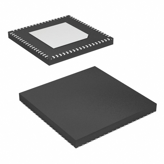


 工商网监
湘ICP备2023018690号
工商网监
湘ICP备2023018690号

