DCV010505, DCV010505D, DCV010512, DCV010512D, DCV010515, DCV010515D, DCV011512D,
DCV011515D, DCV012405, DCV012415D
SBVS014C – AUGUST 2000 – REVISED AUGUST 2021
DCV01 Series, 1-W, 1500-VRMS Isolated, Unregulated DC/DC Converter Modules
1 Features
3 Description
•
•
The DCV01 series is a family of 1-W, 1500-Vrms
isolated, unregulated DC/DC converter modules.
Requiring a minimum of external components and
including on-chip device protection, the DCV01 series
of devices provide extra features such as output
disable and synchronization of switching frequencies.
•
•
•
•
•
•
•
•
•
1.5-kV Isolation (operational): 1-second test
Continuous voltage applied across isolation
barrier: 60 VDC / 42.5 VAC
UL1950 recognized component
EN55022 class B EMC performance
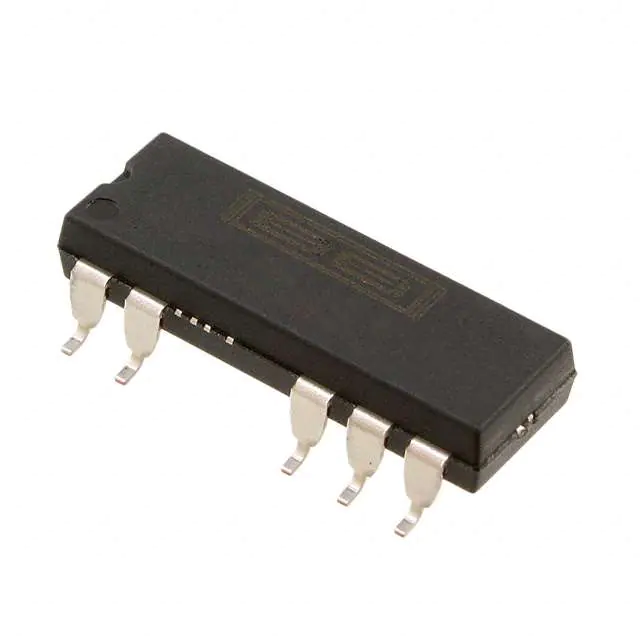
7-Pin PDIP and 7-pin SOP packages
Input voltage: 5 V, 15 V, or 24 V
Output voltage: ±5 V, ±12 V, or ±15 V
Device-to-device synchronization
Thermal protection
Short-circuit protected
High efficiency
This combination of features and small size makes
the DCV01 series of devices suitable for a wide
range of applications, and is an easy-to-use solution
in applications requiring signal path isolation.
WARNING: This product has operational isolation and is intended
for signal isolation only. It must not be used as a part of a safety
isolation circuit requiring reinforced isolation. See definitions in
Section 8.3.
2 Applications
•
•
•
•
•
Signal path isolation
Ground loop elimination
Data acquisition
Industrial control and instrumentation
Test equipment
Device Information
PACKAGE(1)
PART NUMBER
DCV01xxxx
(1)
19.18 mm × 10.60 mm
SOP (7)
19.18 mm × 10.60 mm
For all available packages, see the orderable addendum at
the end of the data sheet.
SYNCOUT
SYNCIN
Oscillator
800 kHz
Divide-by-2
Reset
Watchdog
Startup
SYNCOUT
+VOUT
Power
Stage
BODY SIZE (NOM)
PDIP (7)
SYNCIN
Oscillator
800 kHz
Divide-by-2
Reset
±VOUT
Watchdog
Startup
+VOUT
Power
Stage
±VOUT
COM
Thermal
Shutdown
+VS
PSU Thermal
Shutdown
+VS
Power Controller
±VS
Single Output Block Diagram
Power Controller
±VS
Dual Output Block Diagram
An IMPORTANT NOTICE at the end of this data sheet addresses availability, warranty, changes, use in safety-critical applications,
intellectual property matters and other important disclaimers. PRODUCTION DATA.
�DCV010505, DCV010505D, DCV010512, DCV010512D, DCV010515, DCV010515D, DCV011512D,
DCV011515D, DCV012405, DCV012415D
SBVS014C – AUGUST 2000 – REVISED AUGUST 2021
www.ti.com
Table of Contents
1 Features............................................................................1
2 Applications..................................................................... 1
3 Description.......................................................................1
4 Revision History.............................................................. 2
5 Device Comparison Table...............................................3
6 Pin Configuration and Functions...................................3
7 Specifications.................................................................. 5
7.1 Absolute Maximum Ratings........................................ 5
7.2 ESD Ratings............................................................... 5
7.3 Recommended Operating Conditions.........................5
7.4 Thermal Information....................................................5
7.5 Electrical Characteristics.............................................6
7.6 Switching Characteristics............................................6
7.7 Typical Characteristics................................................ 7
8 Detailed Description...................................................... 11
8.1 Overview................................................................... 11
8.2 Functional Block Diagrams....................................... 11
8.3 Feature Description...................................................12
8.4 Device Functional Modes..........................................14
9 Application and Implementation.................................. 17
9.1 Application Information............................................. 17
9.2 Typical Application.................................................... 17
10 Power Supply Recommendations..............................20
11 Layout........................................................................... 21
11.1 Layout Guidelines................................................... 21
11.2 Layout Example...................................................... 21
12 Device and Documentation Support..........................23
12.1 Device Support....................................................... 23
12.2 Documentation Support.......................................... 23
12.3 Receiving Notification of Documentation Updates..23
12.4 Support Resources................................................. 23
12.5 Trademarks............................................................. 23
12.6 Electrostatic Discharge Caution..............................23
12.7 Glossary..................................................................23
13 Mechanical, Packaging, and Orderable
Information.................................................................... 23
4 Revision History
Changes from Revision B (September 2016) to Revision C (August 2021)
Page
• Updated the numbering format for tables, figures, and cross-references throughout the document. ................1
• Updated Section 1 ............................................................................................................................................. 1
• Added links to Section 2 .................................................................................................................................... 1
• Added sentence in Section 8.3.1.3 .................................................................................................................. 12
• Added Section 8.3.6 ........................................................................................................................................ 13
• Added Section 8.3.7 ........................................................................................................................................ 13
• Added Section 8.3.10 ...................................................................................................................................... 14
Changes from Revision A (December 2013) to Revision B (September 2016)
Page
• Changed Features ............................................................................................................................................. 1
• Changed Applications ........................................................................................................................................1
• Added Device Information table, Device Comparison table, ESD Ratings table, Feature Description section,
Device Functional Modes, Application and Implementation section, Power Supply Recommendations section,
Layout section, Device and Documentation Support section, and Mechanical, Packaging, and Orderable
Information section............................................................................................................................................. 1
• Deleted Electrical Characteristics Per Device table............................................................................................6
• Added additional graphs to Typical Characteristics section................................................................................7
• Added Isolation subsection to Feature Description section.............................................................................. 12
• Deleted DCH, DCP, DCR, and DCV Series DC-DC Converters subsection.....................................................12
• Deleted Continuous Voltage subsection........................................................................................................... 12
• Deleted references to DCP, DCR, DCR, and DCH series................................................................................ 12
• Added typical application design to Application Information section................................................................ 17
2
Submit Document Feedback
Copyright © 2021 Texas Instruments Incorporated
Product Folder Links: DCV010505 DCV010505D DCV010512 DCV010512D DCV010515 DCV010515D
DCV011512D DCV011515D DCV012405 DCV012415D
�DCV010505, DCV010505D, DCV010512, DCV010512D, DCV010515, DCV010515D, DCV011512D,
DCV011515D, DCV012405, DCV012415D
www.ti.com
SBVS014C – AUGUST 2000 – REVISED AUGUST 2021
5 Device Comparison Table
at TA = 25°C, +VS = nominal, CIN = 2.2 µF, and COUT = 0.1 µF (unless otherwise noted)
OUTPUT
VOLTAGE
VNOM at VS (TYP) (V)
75% LOAD
INPUT
VOLTAGE
VS (V)
DEVICE NUMBER
DEVICE
OUTPUT
CURRENT
(mA)(3)
LOAD
REGULATION
10% TO 100%
LOAD(1)
NO LOAD
CURRENT
IQ (mA)
0% LOAD
EFFICIENCY
(%)
100% LOAD
BARRIER
CAPACITANCE
CISO (pF)
VISO = 750 Vrms
MIN
TYP
MAX
MIN
TYP
MAX
MAX
TYP
MAX
TYP
TYP
TYP
DCV010505P
DCV010505P-U
4.5
5
5.5
4.75
5
5.25
200
19
31
20
80
3.6
DCV010505DP
DCV010505DP-U
4.5
5
5.5
±4.25
±5
±5.75
200(2)
18
32
22
81
3.8
DCV010512P
DCV010512P-U
4.5
5
5.5
11.4
12
12.6
83
21
38
29
85
5.1
DCV010512DP
DCV010512DP-U
4.5
5
5.5
±11.4
±12
±12.6
83(2)
19
37
40
82
4
DCV010515P
DCV010515P-U
4.5
5
5.5
14.25
15
15.75
66
26
42
34
82
3.8
DCV010515DP
DCV010515DP-U
4.5
5
5.5
±14.25
±15
±15.75
66(2)
19
41
42
85
4.7
DCV011512DP
DCV011512DP-U
13.5
15
16.5
±11.4
±12
±12.6
83 (2)
11
39
19
78
2.5
DCV011515DP
DCV011515DP-U
13.5
15
16.5
±14.25
±15
±15.75
66(2)
12
39
20
80
2.5
DCV012405P
DCV012405P-U
21.6
24
26.4
4.75
5
5.25
200
13
23
14
77
2.5
DCV012415DP
DCV012415DP-U
21.6
24
26.4
±14.25
±15
±15.75
66(2)
10
35
17
76
3.8
(1)
(2)
(3)
Load regulation = (VOUT at 10% load – VOUT at 100%)/VOUT at 75% load
IOUT1 + IOUT2
POUT(max) = 1 W
6 Pin Configuration and Functions
+VS
1
±VS
2
14
SYNCIN
+VS
1
±VS
2
DCV01
14
SYNCIN
8
SYNCOUT
DCV01
±VOUT
5
COM
5
+VOUT
6
+VOUT
6
NC
7
±VOUT
7
8
SYNCOUT
Figure 6-1. NVA, DUA Package 7-Pin PDIP, SOP
(Single-Output) (Top View)
Figure 6-2. NVA, DUA Package 7-Pin PDIP, SOP
(Dual-Output) (Top View)
Table 6-1. Pin Functions
PIN
NAME
SINGLE-OUTPUT
DUAL-OUTPUT
I/O
DESCRIPTION
COM
—
5
O
Output side common
NC
7
—
—
No connection
SYNCIN
14
14
I
Synchronization. Synchronize multiple devices by
connecting the SYNC pins of each. Pulling this pin low
disables the internal oscillator.
SYNCOUT
8
8
O
Synchronization output. Unrectified transformer output
+VOUT
6
6
O
Positive output voltage
Copyright © 2021 Texas Instruments Incorporated
Submit Document Feedback
Product Folder Links: DCV010505 DCV010505D DCV010512 DCV010512D DCV010515 DCV010515D
DCV011512D DCV011515D DCV012405 DCV012415D
3
�DCV010505, DCV010505D, DCV010512, DCV010512D, DCV010515, DCV010515D, DCV011512D,
DCV011515D, DCV012405, DCV012415D
SBVS014C – AUGUST 2000 – REVISED AUGUST 2021
www.ti.com
Table 6-1. Pin Functions (continued)
PIN
NAME
4
I/O
DESCRIPTION
SINGLE-OUTPUT
DUAL-OUTPUT
+VS
1
1
I
Input voltage
–VOUT
5
7
O
Negative output voltage
–VS
2
2
I
Input side common
Submit Document Feedback
Copyright © 2021 Texas Instruments Incorporated
Product Folder Links: DCV010505 DCV010505D DCV010512 DCV010512D DCV010515 DCV010515D
DCV011512D DCV011515D DCV012405 DCV012415D
�DCV010505, DCV010505D, DCV010512, DCV010512D, DCV010515, DCV010515D, DCV011512D,
DCV011515D, DCV012405, DCV012415D
www.ti.com
SBVS014C – AUGUST 2000 – REVISED AUGUST 2021
7 Specifications
7.1 Absolute Maximum Ratings
over operating free-air temperature range (unless otherwise noted)(1)
MIN
Input voltage
MAX
5-V input devices
7
15-V input devices
18
24-V input devices
29
UNIT
V
Lead temperature
PDIP package
Surface temperature of device body or pins
(maximum 10 s)
270
°C
Reflow solder temperature
SOP package
Surface temperature of device body or pins
260
°C
125
°C
Storage temperature, Tstg
(1)
–60
Stresses beyond those listed under Absolute Maximum Ratings may cause permanent damage to the device. These are stress
ratings only, which do not imply functional operation of the device at these or any other conditions beyond those indicated under
Recommended Operating Conditions. Exposure to absolute-maximum-rated conditions for extended periods may affect device
reliability.
7.2 ESD Ratings
VALUE
V(ESD)
(1)
(2)
Electrostatic discharge
Human-body model (HBM), per ANSI/ESDA/JEDEC JS-001(1)
±1000
Charged-device model (CDM), per JEDEC specification JESD22-C101(2)
±250
UNIT
V
JEDEC document JEP155 states that 500-V HBM allows safe manufacturing with a standard ESD control process.
JEDEC document JEP157 states that 250-V CDM allows safe manufacturing with a standard ESD control process.
7.3 Recommended Operating Conditions
over operating free-air temperature range (unless otherwise noted)
MIN
Input voltage
NOM
MAX
5-V input devices
4.5
5
5.5
15-V input devices
13.5
15
16.5
24-V input devices
21.6
24
26.4
Operating temperature
–40
85
UNIT
V
°C
7.4 Thermal Information
THERMAL
METRIC(1)
DCV01
DCV01
NVA (PDIP)
DVB (SOP)
7 PINS
12 PINS
UNIT
RθJA
Junction-to-ambient thermal resistance
61
61
°C/W
RθJC(top)
Junction-to-case (top) thermal resistance
26
26
°C/W
RθJB
Junction-to-board thermal resistance
24
24
°C/W
ψJT
Junction-to-top characterization parameter
7
7
°C/W
ψJB
Junction-to-board characterization parameter
24
24
°C/W
RθJC(bot)
Junction-to-case (bottom) thermal resistance
—
—
°C/W
(1)
For more information about traditional and new thermal metrics, see the Semiconductor and IC Package Thermal Metrics application
report.
Copyright © 2021 Texas Instruments Incorporated
Submit Document Feedback
Product Folder Links: DCV010505 DCV010505D DCV010512 DCV010512D DCV010515 DCV010515D
DCV011512D DCV011515D DCV012405 DCV012415D
5
�DCV010505, DCV010505D, DCV010512, DCV010512D, DCV010515, DCV010515D, DCV011512D,
DCV011515D, DCV012405, DCV012415D
www.ti.com
SBVS014C – AUGUST 2000 – REVISED AUGUST 2021
7.5 Electrical Characteristics
at TA = 25°C, +VS = nominal, CIN = 2.2 µF, COUT = 1 µF (unless otherwise noted)
PARAMETER
TEST CONDITIONS
MIN
TYP
MAX
UNIT
OUTPUT
POUT
Output power
ILOAD = 100% (full load)
VRIPPLE
Output voltage ripple
COUT = 1 µF, ILOAD = 50%
Voltage vs temperature
0.97
W
20
mVPP
–40°C ≤ TA ≤ 25°C
0.046%
°C
25°C ≤ TA ≤ 85°C
0.016%
°C
INPUT
VS
Input voltage
–10%
10%
ISOLATION
Voltage
1-second flash test
VISO
Isolation
Continuous working
voltage across
isolation barrier
1.5
kVrms
dV/dt
500
V/s
Leakage current
30
nA
DC
60
VDC
AC
42.5
VAC
LINE REGULATION
Output voltage
IOUT ≥ 10% load current and constant,
VS (min) to VS (typ)
1%
15%
IOUT ≥ 10% load current and constant,
VS (typ) to VS (max)
1%
15%
RELIABILITY
Demonstrated
TA = 55°C
75
FITS
THERMAL SHUTDOWN
TSD
Die temperature at shutdown
ISD
Shutdown current
150
°C
3
mA
7.6 Switching Characteristics
at TA = 25°C, +VS = nominal, CIN = 2.2 µF, COUT = 1 µF (unless otherwise noted)
PARAMETER
fOSC
Oscillator frequency
VIL
Low-level input voltage, SYNC
ISYNC
Input current, SYNC
tDISABLE
Disable time
CSYNC
(1)
6
Capacitance loading on SYNC
TEST CONDITIONS
MIN
fSW = fOSC/2
TYP
800
0
VSYNC = 2 V
pin(1)
MAX
UNIT
kHz
0.4
V
75
µA
2
µs
External
3
pF
External Synchronization of the DCP01/02 Series of DC/DC Converters describes this configuration.
Submit Document Feedback
Copyright © 2021 Texas Instruments Incorporated
Product Folder Links: DCV010505 DCV010505D DCV010512 DCV010512D DCV010515 DCV010515D
DCV011512D DCV011515D DCV012405 DCV012415D
�DCV010505, DCV010505D, DCV010512, DCV010512D, DCV010515, DCV010515D, DCV011512D,
DCV011515D, DCV012405, DCV012415D
www.ti.com
SBVS014C – AUGUST 2000 – REVISED AUGUST 2021
7.7 Typical Characteristics
at TA = 25°C (unless otherwise noted)
60
60
Standard Limits
Class A
Class B
40
30
20
10
0
Standard Limits
50
Emission Level, Peak (dBµA)
Emission Level, Peak (dBµA)
50
10
40
30
20
10
0
±10
20
0.15
1
Frequency(MHz)
DCV010505
10
±20
0.15
30
125% Load
1
Frequency(MHz)
DCV010505
Figure 7-1. Conducted Emissions
10
30
8% Load
Figure 7-2. Conducted Emissions
5.5
50
5.4
1-mF Ceramic
4.7-mF Ceramic
10-mF Ceramic
45
40
5.3
35
Output Voltage (V)
Ripple (mVPP)
Class A
Class B
30
25
20
15
10
5.2
5.1
5.0
4.9
4.8
4.7
4.6
5
4.5
0
10
20
30
40
50
60
70
80
90
4.4
4.5
100
4.6
4.7
4.8
Load (%)
DCV010505
4.9
5.0
5.1
5.2
5.3
5.4
5.5
Input Voltage (V)
20-MHz BW
DCV010505
Figure 7-3. Output Ripple versus Load
Figure 7-4. Line Regulation
5.8
85
5.7
5.6
Output Voltage (V)
Efficiency (%)
80
75
70
65
5.5
5.4
5.3
5.2
5.1
5.0
4.9
60
4.8
55
10
20
30
40
50
60
70
80
90
100
4.7
10
20
30
DCV010505
Figure 7-5. Efficiency versus Load
Copyright © 2021 Texas Instruments Incorporated
40
50
60
70
80
90
100
Load (%)
Load (%)
DCV010505
Figure 7-6. Load Regulation
Submit Document Feedback
Product Folder Links: DCV010505 DCV010505D DCV010512 DCV010512D DCV010515 DCV010515D
DCV011512D DCV011515D DCV012405 DCV012415D
7
�DCV010505, DCV010505D, DCV010512, DCV010512D, DCV010515, DCV010515D, DCV011512D,
DCV011515D, DCV012405, DCV012415D
www.ti.com
SBVS014C – AUGUST 2000 – REVISED AUGUST 2021
5.8
85
+VOUT
5.7
80
Output Voltage (V)
75
Efficiency (%)
±VOUT
5.6
70
65
5.5
5.4
5.3
5.2
5.1
5.0
4.9
60
4.8
55
10
20
30
40
50
60
70
90
80
4.7
10
100
20
30
40
60
70
80
90
100
90
100
DCV010505D
DCV010505D
Figure 7-8. Load Regulation
Figure 7-7. Efficiency versus Load
90
14.5
85
14.0
Output Voltage (V)
80
Efficiency (%)
50
Load (%)
Load (%)
75
70
65
60
13.5
13.0
12.5
12.0
11.5
55
50
10
20
30
40
50
60
70
90
80
11.0
100
10
20
30
40
Load (%)
50
60
70
80
Load (%)
DCV010512
DCV010512
Figure 7-9. Efficiency versus Load
Figure 7-10. Load Regulation
14.5
85
14.0
80
13.5
13.0
VOUT (V)
Efficiency (%)
75
70
65
12.5
12.0
11.5
60
11.0
55
+VOUT
-VOUT
10.5
10.00
50
10
20
30
40
50
60
70
80
90
100
10
20
30
DCV010512D
Figure 7-11. Efficiency versus Load
8
Submit Document Feedback
40
50
60
70
80
90
100
Load (%)
Load (%)
DCV010512D
Figure 7-12. Load Regulation
Copyright © 2021 Texas Instruments Incorporated
Product Folder Links: DCV010505 DCV010505D DCV010512 DCV010512D DCV010515 DCV010515D
DCV011512D DCV011515D DCV012405 DCV012415D
�DCV010505, DCV010505D, DCV010512, DCV010512D, DCV010515, DCV010515D, DCV011512D,
DCV011515D, DCV012405, DCV012415D
SBVS014C – AUGUST 2000 – REVISED AUGUST 2021
85
17.5
80
17.0
75
16.5
Output Voltage (V)
Efficiency (%)
www.ti.com
70
65
60
16.0
15.5
15.0
14.5
55
50
10
14.0
20
30
40
50
60
70
80
90
10
100
20
30
40
50
60
70
80
90
100
Load (%)
Load (%)
DCV010515
DCV010515
Figure 7-14. Load Regulation
Figure 7-13. Efficiency versus Load
18
90
85
17
75
VOUT (V)
Efficiency (%)
80
70
16
65
15
60
+VOUT
-VOUT
55
14
50
10
20
30
40
50
60
70
80
90
10
100
20
30
40
50
DCV010515D
70
80
90
100
DCV010515D
Figure 7-15. Efficiency versus Load
Figure 7-16. Load Regulation
90
5.60
80
5.50
70
5.40
60
VOUT (V)
Efficiency (%)
60
Load (%)
Load (%)
50
40
5.30
5.20
5.10
30
20
5.00
10
4.90
0
4.80
10
20
30
40
50
60
70
80
90
100
10
20
30
DCV012405
Figure 7-17. Efficiency versus Load
Copyright © 2021 Texas Instruments Incorporated
40
50
60
70
80
100
Load (%)
Load (%)
DCV012405
Figure 7-18. Load Regulation
Submit Document Feedback
Product Folder Links: DCV010505 DCV010505D DCV010512 DCV010512D DCV010515 DCV010515D
DCV011512D DCV011515D DCV012405 DCV012415D
9
�DCV010505, DCV010505D, DCV010512, DCV010512D, DCV010515, DCV010515D, DCV011512D,
DCV011515D, DCV012405, DCV012415D
www.ti.com
SBVS014C – AUGUST 2000 – REVISED AUGUST 2021
13.5
80
+VOUT
75
Output Voltage (V)
65
Efficiency (%)
±VOUT
13.0
70
60
55
50
45
40
12.5
12.0
11.5
11.0
35
30
10
20
30
40
50
60
70
80
90
10.5
10
100
20
30
40
50
60
70
80
90
100
Load (%)
Load (%)
DCV011512D
DCV011512D
Figure 7-20. Load Regulation
Figure 7-19. Efficiency versus Load
17
90
+VOUT
16.5
80
±VOUT
Output Voltage (V)
Efficiency (%)
16
70
60
50
15.5
15
14.5
14
40
13.5
30
10
20
30
40
50
60
70
80
90
13
10
100
20
30
40
50
60
70
80
90
100
Load (%)
Load (%)
DCV011515D
DCV011515D
Figure 7-22. Load Regulation
Figure 7-21. Efficiency versus Load
90
16.5
80
16
+VOUT
Output Voltage (V)
Efficiency (%)
70
60
50
40
±VOUT
15.5
15
14.5
14
30
20
10
13.5
20
30
40
50
60
70
80
90
100
10
20
30
DCV012415D
Figure 7-23. Efficiency versus Load
10
Submit Document Feedback
40
50
60
70
80
90
100
Load (%)
Load (%)
DCV012415D
Figure 7-24. Load Regulation
Copyright © 2021 Texas Instruments Incorporated
Product Folder Links: DCV010505 DCV010505D DCV010512 DCV010512D DCV010515 DCV010515D
DCV011512D DCV011515D DCV012405 DCV012415D
�DCV010505, DCV010505D, DCV010512, DCV010512D, DCV010515, DCV010515D, DCV011512D,
DCV011515D, DCV012405, DCV012415D
www.ti.com
SBVS014C – AUGUST 2000 – REVISED AUGUST 2021
8 Detailed Description
8.1 Overview
The DCV01 offers up to 1 W of isolated, unregulated output power from a 5-V, 15-V, or 24-V input source with
a typical efficiency of up to 86%. This efficiency is achieved through highly integrated packaging technology
and the implementation of a custom power stage and control device. The DCV01 devices are specified for
operational isolation only. The circuit design uses an advanced BiCMOS and DMOS process.
8.2 Functional Block Diagrams
SYNCOUT
SYNCIN
Oscillator
800 kHz
Divide-by-2
Reset
Watchdog
Startup
+VOUT
Power
Stage
±VOUT
Thermal
Shutdown
+VS
Power Controller
±VS
Figure 8-1. Single Output Device
SYNCOUT
SYNCIN
Oscillator
800 kHz
Divide-by-2
Reset
Watchdog
Startup
+VOUT
Power
Stage
±VOUT
COM
PSU Thermal
Shutdown
+VS
Power Controller
±VS
Figure 8-2. Dual Output Device
Copyright © 2021 Texas Instruments Incorporated
Submit Document Feedback
Product Folder Links: DCV010505 DCV010505D DCV010512 DCV010512D DCV010515 DCV010515D
DCV011512D DCV011515D DCV012405 DCV012415D
11
�DCV010505, DCV010505D, DCV010512, DCV010512D, DCV010515, DCV010515D, DCV011512D,
DCV011515D, DCV012405, DCV012415D
SBVS014C – AUGUST 2000 – REVISED AUGUST 2021
www.ti.com
8.3 Feature Description
8.3.1 Isolation
Underwriters Laboratories, UL™ defines several classes of isolation that are used in modern power supplies.
Safety extra low voltage (SELV) is defined by UL (UL1950 E199929) as a secondary circuit which is so
designated and protected that under normal and single fault conditions the voltage between any two accessible
parts, or between an accessible part and the equipment earthing terminal for operational isolation does not
exceed steady state 42.5 VRMS or 60 VDC peak.
8.3.1.1 Operation or Functional Isolation
The type of isolation used in the DCV01 products is referred to as operational or functional isolation. Insulated
wire used in the construction of the transformer acts as the primary isolation barrier. A high-potential (hipot),
one-second duration test (dielectric voltage, withstand test) is a production test used to verify that the isolation
barrier is functioning. Products with operational isolation must never be used as an element in a safety-isolation
system.
8.3.1.2 Basic or Enhanced Isolation
Basic or enhanced isolation is defined by specified creepage and clearance limits between the primary and
secondary circuits of the power supply. Basic isolation is the use of an isolation barrier in addition to the
insulated wire in the construction of the transformer. Input and output circuits must also be physically separated
by specified distances.
Note
The DCV01 products do not provide basic or enhanced isolation.
8.3.1.3 Working Voltage
For a device with operational isolation, the continuous working voltage that can be applied across the device in
normal operation must be less than 42.5 VRMS or 60 VDC. Ensure that both input and output voltages maintain
normal SELV limits.
WARNING
Do not use the device as an element of a safety isolation system that exceeds the SELV limit.
If the device is expected to function correctly with more than 42.5 VRMS or 60 VDC applied continuously across
the isolation barrier, then the circuitry on both sides of the barrier must be regarded as operating at an unsafe
voltage, and further isolation or insulation systems must form a barrier between these circuits and any useraccessible circuitry according to safety standard requirements.
8.3.1.4 Isolation Voltage Rating
The terms Hipot test, flash-tested, withstand voltage, proof voltage, dielectric withstand voltage, and isolation
test voltage all relate to the same thing. These terms describe a test voltage that is applied across a component
for a specified time, to verify the integrity of the isolation barrier of the component. TI’s DCV01 series of DC/DC
converters are all 100% production tested at 1.5 kVrms for one second.
8.3.1.5 Repeated High-Voltage Isolation Testing
Repeated high-voltage isolation testing of a barrier component can degrade the isolation capability, depending
on materials, construction, and environment. The DCV01 series of DC/DC converters have toroidal, enameled,
wire isolation transformers with no additional insulation between the primary and secondary windings. While a
device can be expected to withstand several times the stated test voltage, the isolation capability depends on the
wire insulation. Any material, including this enamel (typically polyurethane), is susceptible to eventual chemical
degradation when subject to very-high applied voltages. Therefore, strictly limit the number of high-voltage tests
12
Submit Document Feedback
Copyright © 2021 Texas Instruments Incorporated
Product Folder Links: DCV010505 DCV010505D DCV010512 DCV010512D DCV010515 DCV010515D
DCV011512D DCV011515D DCV012405 DCV012415D
�DCV010505, DCV010505D, DCV010512, DCV010512D, DCV010515, DCV010515D, DCV011512D,
DCV011515D, DCV012405, DCV012415D
www.ti.com
SBVS014C – AUGUST 2000 – REVISED AUGUST 2021
and repeated high-voltage isolation testing. However, if it is absolutely required, reduce the voltage by 20% from
specified test voltage with a duration limit of one second per test.
8.3.2 Power Stage
The DCV01 series of devices use a push-pull, center-tapped topology. The DCV01 devices switch at 400 kHz
(divide-by-2 from an 800-kHz oscillator).
8.3.3 Oscillator and Watchdog Circuit
The onboard, 800-kHz oscillator generates the switching frequency via a divide-by-2 circuit. The oscillator can be
synchronized to other DCV01 device circuits or an external source, and is used to minimize system noise.
A watchdog circuit monitors the operation of the oscillator circuit. The oscillator can be disabled by pulling the
SYNC pin low. When the SYNC pin goes low, the output pins transition into tri-state mode, which occurs within
2 µs.
8.3.4 Thermal Shutdown
The DCV01 series of devices are protected by a thermal-shutdown circuit.
If the on-chip temperature rises above 150°C, the device shuts down. Normal operation resumes as soon as
the temperature falls below 150°C. While the overtemperature condition continues, operation randomly cycles on
and off. This cycling continues until the temperature is reduced.
8.3.5 Synchronization
When more than one DC/DC converter is needed onboard, beat frequencies and other electrical interference
can be generated. This interference occurs because of the small variations in switching frequencies between the
DC/DC converters.
The DCV01 series of devices overcome this interference by allowing devices to be synchronized to one
another. Synchronize up to eight devices by connecting the SYNC pins of each device, taking care to minimize
the capacitance of tracking. Stray capacitance (greater than 3 pF) reduces the switching frequency, or can
sometimes stop the oscillator circuit. The maximum recommended voltage applied to the SYNC pin is 3 V.
For an application that uses more than eight synchronized devices use an external device to drive the
SYNC pins. External Synchronization of the DCP01/02 Series of DC/DC Converters (SBAA035) describes this
configuration.
Note
During the start-up period, all synchronized devices draw maximum current from the input
simultaneously. If the input voltage falls below approximately 4 V, the devices may not start up. A
ceramic capacitor must be connected close to the input pin of each device. Use a 2.2-µF capacitor for
5-V and 15-V input devices, and a 0.47-µF capacitor for the
24-V devices.
8.3.6 Light Load Operation (< 10%)
Operation below 10% load can cause the output voltage to increase up to double the typical output voltage.
For applications that operate less than 10% of rated output current, it is recommended to add a minimum load
to ensure the output voltage of the device is within the load regulation range. For example, connect a 250-Ω
pre-load resistor to meet the 10% minimum load condition for the DCV010505P.
8.3.7 Load Regulation (10% to 100%)
The load regulation of the DCV01 series of devices are specified at 10% to 100% load. Placing a minimum of
10% load will ensure the output voltage is within the range specified in the Section 7.5. For more information
regarding the operation below 10% load, see Section 8.3.6.
Copyright © 2021 Texas Instruments Incorporated
Submit Document Feedback
Product Folder Links: DCV010505 DCV010505D DCV010512 DCV010512D DCV010515 DCV010515D
DCV011512D DCV011515D DCV012405 DCV012415D
13
�DCV010505, DCV010505D, DCV010512, DCV010512D, DCV010515, DCV010515D, DCV011512D,
DCV011515D, DCV012405, DCV012415D
SBVS014C – AUGUST 2000 – REVISED AUGUST 2021
www.ti.com
8.3.8 Construction
The basic construction of the DCV01 series of devices is the same as standard integrated circuits. The molded
package contains no substrate. The DCV01 series of devices are constructed using an IC, rectifier diodes, and
a wound magnetic toroid on a leadframe. Because the package contains no solder, the devices do not require
any special printed circuit board (PCB) assembly processing. This architecture results in an isolated DC/DC
converter with inherently high reliability.
8.3.9 Thermal Management
Due to the high power density of this device, it is advisable to provide ground planes on the input and output
rails.
8.3.10 Power-Up Characteristics
The DCV01 series of devices do not include a soft-start feature. Therefore, a high in-rush current during
power-up is expected. To ensure a more stable start-up, allow the input voltage to be in regulation before
enabling the device. Refer to the Section 8.4.1 section on how to disable/enable the device. Figure 8-6 shows
the typical start-up waveform for a DCV010505P when enabled after the input voltage is in regulation. Figure 8-3
shows the typical start-up waveform for a DCV010505P, operating from a 5-V input with no load on the output.
Figure 8-4 shows the start-up waveform for a DCV010505P starting up into a 10% load. Figure 8-5 shows the
start-up waveform starting up into a full (100%) load.
Figure 8-3. DCV010505P Start-Up at No Load
Figure 8-4. DCV010505P Start-Up at 10% Load
Figure 8-5. DCV010505P Start-Up at 100% Load
Figure 8-6. DCV010505P Enable Start-Up at 100%
Load
8.4 Device Functional Modes
8.4.1 Disable and Enable (SYNCIN Pin)
Each of the DCV01 series devices can be disabled or enabled by driving the SYNCIN pin using an open-drain
CMOS gate. If the SYNCIN pin is pulled low, the DCV01 becomes disabled. The disable time depends upon
the external loading. The internal disable function is implemented in 2 µs. Removal of the pulldown causes the
DCV01 to be enabled.
14
Submit Document Feedback
Copyright © 2021 Texas Instruments Incorporated
Product Folder Links: DCV010505 DCV010505D DCV010512 DCV010512D DCV010515 DCV010515D
DCV011512D DCV011515D DCV012405 DCV012415D
�DCV010505, DCV010505D, DCV010512, DCV010512D, DCV010515, DCV010515D, DCV011512D,
DCV011515D, DCV012405, DCV012415D
www.ti.com
SBVS014C – AUGUST 2000 – REVISED AUGUST 2021
Capacitive loading on the SYNCIN pin must be minimized (≤ 3 pF) in order to prevent a reduction in the
oscillator frequency. The External Synchronization of the DCP01/02 Series of DC/DC Converters application
report (SBAA035) describes disable/enable control circuitry.
8.4.2 Decoupling
8.4.2.1 Ripple Reduction
The high switching frequency of 400 kHz allows simple filtering. To reduce ripple, TI recommends that a
minimum of 1-µF capacitor be used on the +VOUT pin. For dual output devices, decouple both of the outputs to
the COM pin. The required 2.2-µF, low ESR ceramic input capacitor also helps to reduce ripple and noise, (24-V
input voltage versions require only 0.47 µF of input capacitance). See the DC-to-DC Converter Noise Reduction
application report (SBVA012).
8.4.2.2 Connecting the DCV01 in Series
Multiple DCV01 devices can be connected in series to provide non-standard voltage rails. This configuration is
possible by using the floating outputs provided by the galvanic isolation of the DCV01.
Connect the +VOUT from one DCV01 to the –VOUT of another (see Figure 8-7). If the SYNCIN pins are tied
together, the self-synchronization feature of the DCV01 prevents beat frequencies on the voltage rails. The
synchronization feature of the DCV01 allows easy series connection without external filtering, thus minimizing
cost.
VIN
+VOUT1
+VS
CIN
SYNCIN
CIN
DCV
COUT
1.0 µF
01
±VS
±VOUT1
VS
+VOUT2
SYNCIN
DCV
±VS
VOUT1
+
VOUT2
COUT
1.0 µF
01
±VOUT2
Figure 8-7. Multiple DCV01 Devices Connected in Series
The outputs of a dual-output DCV01 can also be connected in series to provide two times the magnitude of
+VOUT, as shown in Figure 8-8. For example, connect a dual-output, 15-V, DCP012415D device to provide a
30-V rail.
VIN
+VOUT
+VS
CIN
DCV
+VOUT
COUT
1.0 µF
01
±VOUT
±VOUT
±VS
COM
COUT
1.0 µF
Figure 8-8. Dual Output Devices Connected in Series
8.4.2.3 Connecting the DCV01 in Parallel
If the output power from one DCV01 is not sufficient, it is possible to parallel the outputs of multiple DCV01s,
as shown in Figure 8-9 (applies to single output devices only). The synchronization feature allows easy
synchronization to prevent power-rail beat frequencies at no additional filtering cost.
Copyright © 2021 Texas Instruments Incorporated
Submit Document Feedback
Product Folder Links: DCV010505 DCV010505D DCV010512 DCV010512D DCV010515 DCV010515D
DCV011512D DCV011515D DCV012405 DCV012415D
15
�DCV010505, DCV010505D, DCV010512, DCV010512D, DCV010515, DCV010515D, DCV011512D,
DCV011515D, DCV012405, DCV012415D
SBVS014C – AUGUST 2000 – REVISED AUGUST 2021
VIN
+VOUT1
+VS
SYNCIN
CIN
www.ti.com
DCV
01
±VS
COUT
1.0 µF
±VOUT1
2 × Power Out
+VOUT2
+VS
CIN
SYNCIN
±VS
DCV
COUT
1.0 µF
01
±VOUT2
GND
Figure 8-9. Multiple DCV01 Devices Connected in Parallel
16
Submit Document Feedback
Copyright © 2021 Texas Instruments Incorporated
Product Folder Links: DCV010505 DCV010505D DCV010512 DCV010512D DCV010515 DCV010515D
DCV011512D DCV011515D DCV012405 DCV012415D
�DCV010505, DCV010505D, DCV010512, DCV010512D, DCV010515, DCV010515D, DCV011512D,
DCV011515D, DCV012405, DCV012415D
www.ti.com
SBVS014C – AUGUST 2000 – REVISED AUGUST 2021
9 Application and Implementation
Note
Information in the following applications sections is not part of the TI component specification,
and TI does not warrant its accuracy or completeness. TI’s customers are responsible for
determining suitability of components for their purposes, as well as validating and testing their design
implementation to confirm system functionality.
9.1 Application Information
The DCV01 devices offer up to 1 W of isolated, unregulated output power from a 5-V, 15-V, or 24-V input supply.
Applications requiring up to 1.5-kVrms of operational isolation benefit from the small size and ease-of-use of the
DCV01 family of devices.
9.2 Typical Application
VIN
+VS
CIN
2.2 µF
SYNC
+VOUT
+VOUT
DCV01
±VS
COUT
1.0 µF
±VOUT
±VOUT
Copyright © 2016, Texas Instruments Incorporated
Figure 9-1. DCV010505 Typical Application Schematic
9.2.1 Design Requirements
For this design example, use the parameters listed in Table 9-1 and follow the procedures in the Section 9.2.2.
Table 9-1. Design Example Parameters
PARAMETER
VALUE
V(+VS)
Input voltage
5V
V(+VOUT)
Output voltage
5V
IOUT
Output current rating
200 mA
fSW
Operating frequency
400 kHz
9.2.2 Detailed Design Procedure
9.2.2.1 Input Capacitor
For all 5-V and 15-V input voltage designs, select a 2.2-µF low-ESR ceramic input capacitor to ensure a good
start-up performance. 24-V input applications require only 0.47 µF of input capacitance.
9.2.2.2 Output Capacitor
For any DCV01 design, select a 1-µF low-ESR ceramic output capacitor to reduce output ripple.
9.2.2.3 SYNCIN Pin
In a stand-alone application, leave the SYNCIN pin floating.
9.2.2.4 PCB Design
The copper losses (resistance and inductance) can be minimized by using wide ground and power traces or
planes. If several devices are being powered from a common power source, a star-connected layout must be
used. Device inputs must not be connected in series, as this will cascade the resistive losses. The position of the
Copyright © 2021 Texas Instruments Incorporated
Submit Document Feedback
Product Folder Links: DCV010505 DCV010505D DCV010512 DCV010512D DCV010515 DCV010515D
DCV011512D DCV011515D DCV012405 DCV012415D
17
�DCV010505, DCV010505D, DCV010512, DCV010512D, DCV010515, DCV010515D, DCV011512D,
DCV011515D, DCV012405, DCV012415D
SBVS014C – AUGUST 2000 – REVISED AUGUST 2021
www.ti.com
decoupling capacitors is important to reduce losses. Place the decoupling capacitors as close to the devices as
possible. See the PCB Layout for more details.
9.2.2.5 Decoupling Ceramic Capacitors
Capacitor Impedance (Ÿ )
All capacitors have losses because of internal equivalent series resistance (ESR), and to a lesser degree,
equivalent series inductance (ESL). Values for ESL are not always easy to obtain. However, some
manufacturers provide graphs of frequency versus capacitor impedance. These graphs typically show the
capacitor impedance falling as frequency is increased (as shown in Figure 9-2). In Figure 9-2, XC is the
reactance due to the capacitance, XL is the reactance due to the ESL, and f0 is the resonant frequency. As
the frequency increases, the impedance stops decreasing and begins to rise. The point of minimum impedance
indicates the resonant frequency of the capacitor. This frequency is where the components of capacitance and
inductance reactance are of equal magnitude. Beyond this point, the capacitor is not effective as a capacitor.
Z
XC
XL
0
Frequency (Hz)
f0
Figure 9-2. Capacitor Impedance versus Frequency
At f0, XC = XL; however, there is a 180° phase difference resulting in cancellation of the imaginary component.
The resulting effect is that the impedance at the resonant point is the real part of the complex impedance;
namely, the value of the ESR. The resonant frequency must be well above the 800-kHz switching frequency of
the device.
The effect of the ESR is to cause a voltage drop within the capacitor. The value of this voltage drop is simply the
product of the ESR and the transient load current, as shown in Equation 1.
VIN = VPK – (ESR × ITR)
(1)
where
•
•
•
VIN is the voltage at the device input
VPK is the maximum value of the voltage on the capacitor during charge
ITR is the transient load current
The other factor that affects the performance is the value of the capacitance. However, for the input and the full
wave outputs (single-output voltage devices), ESR is the dominant factor.
9.2.2.6 Input Capacitor and the Effects of ESR
If the input decoupling capacitor is not ceramic (and has an ESR greater than 20 mΩ), then at the instant
the power transistors switch on, the voltage at the input pins falls momentarily. If the voltage falls below
approximately 4 V, the DCV01 detects an undervoltage condition and switches the DCV01 drive circuits to a
momentary off state. This detection is carried out as a precaution against a genuine low input voltage condition
that could slow down or even stop the internal circuits from operating correctly. A slow-down or stoppage results
in the drive transistors being turned on too long, causing saturation of the transformer and destruction of the
device.
Following detection of a low input voltage condition, the device switches off the internal drive circuits until the
input voltage returns to a safe value, at which time the device tries to restart. If the input capacitor is still unable
to maintain the input voltage, shutdown recurs. This process repeats until the input capacitor charges sufficiently
to start the device correctly.
18
Submit Document Feedback
Copyright © 2021 Texas Instruments Incorporated
Product Folder Links: DCV010505 DCV010505D DCV010512 DCV010512D DCV010515 DCV010515D
DCV011512D DCV011515D DCV012405 DCV012415D
�www.ti.com
DCV010505, DCV010505D, DCV010512, DCV010512D, DCV010515, DCV010515D, DCV011512D,
DCV011515D, DCV012405, DCV012415D
SBVS014C – AUGUST 2000 – REVISED AUGUST 2021
Normal start-up must occur in approximately 1 ms after power is applied to the device. If a considerably longer
start-up duration time is encountered, it is likely that either (or both) the input supply or the capacitors are not
performing adequately.
For 5-V to 15-V input devices, a 2.2-µF, low-ESR ceramic capacitor ensures a good start-up performance. For
24-V input voltage devices, TI recommends 0.47-µF ceramic capacitors. Tantalum capacitors are not
recommended, because most do not have low-ESR values and will degrade performance. If tantalum capacitors
must be used, designers must pay close attention to both the ESR and voltage as derated by the vendor.
Note
During the start-up period, these devices can draw maximum current from the input supply. If the
input voltage falls below approximately 4 V, the devices may not start up. Connect a 2.2-µF ceramic
capacitor close to the input pins.
9.2.2.7 Ripple and Noise
A good quality, low-ESR ceramic capacitor placed as close as possible across the input reduces reflected ripple
and ensures a smooth start-up.
A good quality, low-ESR ceramic capacitor placed as close as possible across the rectifier output terminal
and output ground gives the best ripple and noise performance. See the DC-to-DC Converter Noise Reduction
application report (SBVA012) for more information on noise rejection.
9.2.2.7.1 Output Ripple Calculation Example
The following example shows that increasing the capacitance has a much smaller effect on the output ripple
voltage than does reducing the value of the ESR for the filter capacitor.
To calculate the output ripple for a DCV010505 device:
•
•
•
•
•
•
•
•
•
•
VOUT = 5 V
IOUT = 0.2 A
At full output power, the load resistor is 25 Ω
Output capacitor of 1 µF, ESR of 0.1 Ω
Capacitor discharge time 1% of 800 kHz (ripple frequency)
tDIS = 0.0125 µs
τ = C × RLOAD
τ = 1 × 10-6 × 25 = 25 µs
VDIS = VO(1 – EXP(–tDIS / τ))
VDIS = 2.5 mV
By contrast, the voltage dropped because of ESR:
•
•
•
VESR = ILOAD × ESR
VESR = 0.2 × 0.1 = 20 mV
Ripple voltage = 22.5 mV
9.2.2.8 Dual DCV01 Output Voltage
The voltage output for dual DCV01 devices is half-wave rectified; therefore, the discharge time is 1.25 µs.
Repeating the previous calculations using the 100% load resistance of 50 Ω (0.1 A per output), the results are:
•
•
•
•
•
τ = 50 µs
tDIS = 1.25 µs
VDIS = 123 mV
VESR = 0.1 × 0.1 = 10 mV
Ripple Voltage = 133 mV
In this example, it is the capacitor discharging that contributes to the largest component of ripple. Changing the
output filter to 10 µF, and repeating the calculations, the result is that the ripple voltage is 22.3 mV.
This value is composed of almost equal components.
Copyright © 2021 Texas Instruments Incorporated
Submit Document Feedback
Product Folder Links: DCV010505 DCV010505D DCV010512 DCV010512D DCV010515 DCV010515D
DCV011512D DCV011515D DCV012405 DCV012415D
19
�DCV010505, DCV010505D, DCV010512, DCV010512D, DCV010515, DCV010515D, DCV011512D,
DCV011515D, DCV012405, DCV012415D
www.ti.com
SBVS014C – AUGUST 2000 – REVISED AUGUST 2021
The previous calculations are offered as a guideline only. Capacitor parameters usually have large tolerances
and can be susceptible to environmental conditions.
9.2.2.9 Optimizing Performance
Optimum performance can only be achieved if the device is correctly supported. The very nature of a switching
converter requires power to be instantly available when it switches on. If the converter has DMOS switching
transistors, the fast edges create a high current demand on the input supply. This transient load placed on the
input is supplied by the external input decoupling capacitor, thus maintaining the input voltage. Therefore, the
input supply does not experience this transient (this is analogous to high-speed digital circuits). The positioning
of the capacitor is critical and must be placed as close as possible to the input pins and connected through a
low-impedance path.
The optimum performance primarily depends on two factors:
•
•
Connection of the input and output circuits for minimal loss.
The ability of the decoupling capacitors to maintain the input and output voltages at a constant level.
9.2.3 Application Curves
5.8
85
5.7
80
5.6
Output Voltage (V)
Efficiency (%)
75
70
65
60
5.5
5.4
5.3
5.2
5.1
5.0
4.9
55
4.8
50
10
20
30
40
50
60
70
80
90
100
4.7
10
20
30
DCV010505
Figure 9-3. Efficiency versus Load
40
50
60
70
80
90
100
Load (%)
Load (%)
DCV010515
Note: Operations under 10% Load
Figure 9-4. Load Regulation
10 Power Supply Recommendations
The DCV01 is a switching power supply, and as such can place high peak current demands on the input supply.
To avoid the supply falling momentarily during the fast switching pulses, ground and power planes must be
used to connect the power to the input of DCV01. If this connection is not possible, then the supplies must be
connected in a star formation with the traces made as wide as possible.
20
Submit Document Feedback
Copyright © 2021 Texas Instruments Incorporated
Product Folder Links: DCV010505 DCV010505D DCV010512 DCV010512D DCV010515 DCV010515D
DCV011512D DCV011515D DCV012405 DCV012415D
�www.ti.com
DCV010505, DCV010505D, DCV010512, DCV010512D, DCV010515, DCV010515D, DCV011512D,
DCV011515D, DCV012405, DCV012415D
SBVS014C – AUGUST 2000 – REVISED AUGUST 2021
11 Layout
11.1 Layout Guidelines
Due to the high power density of these devices, provide ground planes on the input and output.
Figure 11-1 shows a schematic for two DCV01 devices. Figure 11-2 and Figure 11-3 show a typical layout for two
through-hole PDIP devices.
Input power and ground planes provide a low-impedance path for the input power. For the output, the COM
signal connects through a ground plane, while the connections for the positive and negative voltage outputs
conduct through wide traces to minimize losses.
The output must be taken from the device using ground and power planes, thereby ensuring minimum losses.
The location of the decoupling capacitors in close proximity to their respective pins ensures low losses due to
the effects of stray inductance, thus improving the ripple performance. This location is of particular importance
to the input decoupling capacitor, because this capacitor supplies the transient current associated with the fast
switching waveforms of the power drive circuits.
Allow the unused SYNC pin, to remain configured as a floating pad. It is advisable to place a guard ring
(connected to input ground) or annulus connected around this pin to avoid any noise pickup. When connecting
a SYNC pin to one or more SYNC design the linking trace to be short and narrow to avoid stray capacitance.
Ensure that no other trace is in close proximity to this trace SYNC trace to decrease the stray capacitance on
this pin. The stray capacitance affects the performance of the oscillator.
11.2 Layout Example
CON1
VS1
1
+VS SYNC 14
2
±VS
JP1
C1
0V1
DCV01
+V1
C3
C2-1
6
+VOUT
5
COM
7
±VOUT
C2
R1
COM1
C5
C4-1
C4
R2
± V1
CON2
VS2
1
+VS SYNC 14
2
±VS
JP2
C6
0V2
DCV01
+V2
C8
C7-1
6
+VOUT
5
COM
7
±VOUT
C7
R3
COM2
C10
C9-1
C9
R4
± V2
Figure 11-1. PCB Schematic, P and U Package
Copyright © 2021 Texas Instruments Incorporated
Submit Document Feedback
Product Folder Links: DCV010505 DCV010505D DCV010512 DCV010512D DCV010515 DCV010515D
DCV011512D DCV011515D DCV012405 DCV012415D
21
�DCV010505, DCV010505D, DCV010512, DCV010512D, DCV010515, DCV010515D, DCV011512D,
DCV011515D, DCV012405, DCV012415D
SBVS014C – AUGUST 2000 – REVISED AUGUST 2021
Figure 11-2. PCB Layout Example, ComponentSide View
22
Submit Document Feedback
www.ti.com
Figure 11-3. PCB Layout Example, NonComponent-Side View
Copyright © 2021 Texas Instruments Incorporated
Product Folder Links: DCV010505 DCV010505D DCV010512 DCV010512D DCV010515 DCV010515D
DCV011512D DCV011515D DCV012405 DCV012415D
�DCV010505, DCV010505D, DCV010512, DCV010512D, DCV010515, DCV010515D, DCV011512D,
DCV011515D, DCV012405, DCV012415D
www.ti.com
SBVS014C – AUGUST 2000 – REVISED AUGUST 2021
12 Device and Documentation Support
12.1 Device Support
12.1.1 Device Nomenclature
DCV01
05
05
(D)
(P)
Basic model number: 1-W product
Voltage input:
5, 15, or 24
Voltage output:
5, 12 or 15
Output type:
blank (single) or D (dual)
Package code:
P = 7-pin PDIP (NVA package)
P-U = 7-pin SOP (DUA package)
Figure 12-1. Supplemental Ordering Information
12.2 Documentation Support
12.2.1 Related Documentation
For related documentation see the following:
•
•
•
Texas Instruments, External Synchronization of the DCP01/02 Series of DC/DC Converters (SBAA035)
Texas Instruments, DC-to-DC Converter Noise Reduction (SBVA012)
Texas Instruments, Optimizing Performance of the DCP01/02 Series of DC/DC Converters (SBVA013)
12.3 Receiving Notification of Documentation Updates
To receive notification of documentation updates, navigate to the device product folder on ti.com. Click on
Subscribe to updates to register and receive a weekly digest of any product information that has changed. For
change details, review the revision history included in any revised document.
12.4 Support Resources
TI E2E™ support forums are an engineer's go-to source for fast, verified answers and design help — straight
from the experts. Search existing answers or ask your own question to get the quick design help you need.
Linked content is provided "AS IS" by the respective contributors. They do not constitute TI specifications and do
not necessarily reflect TI's views; see TI's Terms of Use.
12.5 Trademarks
Underwriters Laboratories, UL™ is a trademark of UL LLC.
TI E2E™ is a trademark of Texas Instruments.
All trademarks are the property of their respective owners.
12.6 Electrostatic Discharge Caution
This integrated circuit can be damaged by ESD. Texas Instruments recommends that all integrated circuits be handled
with appropriate precautions. Failure to observe proper handling and installation procedures can cause damage.
ESD damage can range from subtle performance degradation to complete device failure. Precision integrated circuits may
be more susceptible to damage because very small parametric changes could cause the device not to meet its published
specifications.
12.7 Glossary
TI Glossary
This glossary lists and explains terms, acronyms, and definitions.
13 Mechanical, Packaging, and Orderable Information
The following pages include mechanical, packaging, and orderable information. This information is the most
current data available for the designated devices. This data is subject to change without notice and revision of
this document. For browser-based versions of this data sheet, refer to the left-hand navigation.
Copyright © 2021 Texas Instruments Incorporated
Submit Document Feedback
Product Folder Links: DCV010505 DCV010505D DCV010512 DCV010512D DCV010515 DCV010515D
DCV011512D DCV011515D DCV012405 DCV012415D
23
�PACKAGE OPTION ADDENDUM
www.ti.com
10-Dec-2020
PACKAGING INFORMATION
Orderable Device
Status
(1)
Package Type Package Pins Package
Drawing
Qty
Eco Plan
(2)
Lead finish/
Ball material
MSL Peak Temp
Op Temp (°C)
(3)
Device Marking
(4/5)
(6)
DCV010505DP
ACTIVE
PDIP
NVA
7
25
RoHS &
Non-Green
NIPDAU
N / A for Pkg Type
-40 to 85
DCV010505DP
DCV010505DP-U
ACTIVE
SOP
DUA
7
25
RoHS &
Non-Green
NIPDAU
Level-3-260C-168 HR
-40 to 85
DCV010505DP-U
DCV010505P
ACTIVE
PDIP
NVA
7
25
RoHS &
Non-Green
NIPDAU
N / A for Pkg Type
-40 to 85
DCV010505P
DCV010505P-U
ACTIVE
SOP
DUA
7
25
RoHS &
Non-Green
NIPDAU
Level-3-260C-168 HR
-40 to 85
DCV010505P-U
DCV010505P-U/700
ACTIVE
SOP
DUA
7
700
RoHS &
Non-Green
NIPDAU
Level-3-260C-168 HR
-40 to 85
DCV010505P-U
DCV010512DP
ACTIVE
PDIP
NVA
7
25
RoHS &
Non-Green
NIPDAU
N / A for Pkg Type
-40 to 85
DCV010512DP
DCV010512DP-U
ACTIVE
SOP
DUA
7
25
RoHS &
Non-Green
NIPDAU
Level-3-260C-168 HR
-40 to 85
DCV10512DPU
DCV010512P
ACTIVE
PDIP
NVA
7
25
RoHS &
Non-Green
NIPDAU
N / A for Pkg Type
-40 to 85
DCV010512P
DCV010512P-U
ACTIVE
SOP
DUA
7
25
RoHS &
Non-Green
NIPDAU
Level-3-260C-168 HR
-40 to 85
DCV010512P-U
DCV010515DP
ACTIVE
PDIP
NVA
7
25
RoHS &
Non-Green
NIPDAU
N / A for Pkg Type
-40 to 85
DCV010515DP
DCV010515DP-U
ACTIVE
SOP
DUA
7
25
RoHS &
Non-Green
NIPDAU
Level-3-260C-168 HR
-40 to 85
DCV010515DP-U
DCV010515P
ACTIVE
PDIP
NVA
7
25
RoHS &
Non-Green
NIPDAU
N / A for Pkg Type
-40 to 85
DCV010515P
DCV010515P-U
ACTIVE
SOP
DUA
7
25
RoHS &
Non-Green
NIPDAU
Level-3-260C-168 HR
-40 to 85
DCV010515P-U
DCV011512DP
ACTIVE
PDIP
NVA
7
25
RoHS &
Non-Green
NIPDAU
N / A for Pkg Type
-40 to 85
DCV011512DP
DCV011512DP-U
ACTIVE
SOP
DUA
7
25
RoHS &
Non-Green
NIPDAU
Level-3-260C-168 HR
-40 to 85
DCV011512DP-U
DCV011515DP
ACTIVE
PDIP
NVA
7
25
RoHS &
Non-Green
NIPDAU
N / A for Pkg Type
-40 to 85
DCV011515DP
Addendum-Page 1
Samples
�PACKAGE OPTION ADDENDUM
www.ti.com
10-Dec-2020
Orderable Device
Status
(1)
Package Type Package Pins Package
Drawing
Qty
Eco Plan
(2)
Lead finish/
Ball material
MSL Peak Temp
Op Temp (°C)
(3)
Device Marking
(4/5)
(6)
DCV011515DP-U
ACTIVE
SOP
DUA
7
25
RoHS &
Non-Green
NIPDAU
Level-3-260C-168 HR
-40 to 85
DCV011515DP-U
DCV011515DP-U/700
ACTIVE
SOP
DUA
7
700
RoHS &
Non-Green
NIPDAU
Level-3-260C-168 HR
-40 to 85
DCV011515DP-U
DCV012405P
ACTIVE
PDIP
NVA
7
25
RoHS &
Non-Green
NIPDAU
N / A for Pkg Type
-40 to 85
DCV012405P
DCV012405P-U
ACTIVE
SOP
DUA
7
25
RoHS &
Non-Green
NIPDAU
Level-3-260C-168 HR
-40 to 85
DCV012405P-U
DCV012415DP
ACTIVE
PDIP
NVA
7
25
RoHS &
Non-Green
NIPDAU
N / A for Pkg Type
-40 to 85
DCV012415DP
DCV012415DP-U
ACTIVE
SOP
DUA
7
25
RoHS &
Non-Green
NIPDAU
Level-3-260C-168 HR
-40 to 85
DCV012415DP-U
DCV012415DP-U/700
ACTIVE
SOP
DUA
7
700
RoHS &
Non-Green
NIPDAU
Level-3-260C-168 HR
-40 to 85
DCV012415DP-U
(1)
The marketing status values are defined as follows:
ACTIVE: Product device recommended for new designs.
LIFEBUY: TI has announced that the device will be discontinued, and a lifetime-buy period is in effect.
NRND: Not recommended for new designs. Device is in production to support existing customers, but TI does not recommend using this part in a new design.
PREVIEW: Device has been announced but is not in production. Samples may or may not be available.
OBSOLETE: TI has discontinued the production of the device.
(2)
RoHS: TI defines "RoHS" to mean semiconductor products that are compliant with the current EU RoHS requirements for all 10 RoHS substances, including the requirement that RoHS substance
do not exceed 0.1% by weight in homogeneous materials. Where designed to be soldered at high temperatures, "RoHS" products are suitable for use in specified lead-free processes. TI may
reference these types of products as "Pb-Free".
RoHS Exempt: TI defines "RoHS Exempt" to mean products that contain lead but are compliant with EU RoHS pursuant to a specific EU RoHS exemption.
Green: TI defines "Green" to mean the content of Chlorine (Cl) and Bromine (Br) based flame retardants meet JS709B low halogen requirements of


 工商网监
湘ICP备2023018690号
工商网监
湘ICP备2023018690号

