DP8392C,DP8392C-1
DP8392C DP8392C-1 CTI Coaxial Transceiver Interface
Literature Number: SNLS078A
�DP8392C/DP8392C-1 CTI
Coaxial Transceiver Interface
General Description
Features
The DP8392C Coaxial Transceiver Interface (CTI) is a coaxial cable line driver/receiver for Ethernet/Thin Ethernet
(Cheapernet) type local area networks. The CTI is connected between the coaxial cable and the Data Terminal Equipment (DTE). In Ethernet applications the transceiver is usually mounted within a dedicated enclosure and is connected
to the DTE via a transceiver cable. In Cheapernet applications, the CTI is typically located within the DTE and connects to the DTE through isolation transformers only. The
CTI consists of a Receiver, Transmitter, Collision Detector,
and a Jabber Timer. The Transmitter connects directly to a
50 ohm coaxial cable where it is used to drive the coax
when transmitting. During transmission, a jabber timer is initiated to disable the CTI transmitter in the event of a longer
than legal length data packet. Collision Detection circuitry
monitors the signals on the coax to determine the presence
of colliding packets and signals the DTE in the event of a
collision.
The CTI is part of a three chip set that implements the complete IEEE 802.3 compatible network node electronics as
shown below. The other two chips are the DP8391 Serial
Network Interface (SNI) and the DP8390 Network Interface
Controller (NIC).
The SNI provides the Manchester encoding and decoding
functions; whereas the NIC handles the Media Access Protocol and the buffer management tasks. Isolation between
the CTI and the SNI is an IEEE 802.3 requirement that can
be easily satisfied on signal lines using a set of pulse transformers that come in a standard DIP. However, the power
isolation for the CTI is done by DC-to-DC conversion
through a power transformer.
Y
Y
Y
Y
Y
Y
Y
et
Y
e
Y
Compatible with Ethernet II, IEEE 802.3 10Base5 and
10Base2 (Cheapernet)
Integrates all transceiver electronics except signal &
power isolation
Innovative design minimizes external component count
Jabber timer function integrated on chip
Externally selectable CD Heartbeat allows operation
with IEEE 802.3 compatible repeaters
Precision circuitry implements receive mode collision
detection
Squelch circuitry at all inputs rejects noise
Designed for rigorous reliability requirements of
IEEE 802.3
Standard Outline 16-pin DIP uses a special leadframe
that significantly reduces the operating die temperature
Table of Contents
bs
ol
1.0 System Diagram
2.0 Block Diagram
3.0 Functional Description
3.1 Receiver Functions
3.2 Transmitter Functions
3.3 Collision Functions
3.4 Jabber Functions
4.0 Typical Applications
5.0 Connection Diagrams
6.0 Pin Descriptions
7.0 Absolute Maximum Ratings
8.0 DP8392C Electrical Characteristics
9.0 DP8392C-1 Electrical Characteristics
10.0 Switching Characteristics
11.0 Timing and Load Diagram
O
1.0 System Diagram
TL/F/11085 – 1
IEEE 802.3 Compatible Ethernet/Cheapernet Local Area Network Chip Set
C1995 National Semiconductor Corporation
TL/F/11085
RRD-B30M115/Printed in U. S. A.
DP8392C/DP8392C-1 CTI Coaxial Transceiver Interface
October 1995
�et
e
2.0 Block Diagram
TL/F/11085 – 2
FIGURE 1. DP8392C Block Diagram
3.0 Functional Description
Receiver then stays off only if within about 1 ms, the DC
level from the low pass filter rises above the DC squelch
threshold. Figure 2 illustrates the Receiver timing.
The differential line driver provides ECL compatible signals
to the DTE with typically 3 ns rise and fall times. In its idle
state, its outputs go to differential zero to prevent DC standing current in the isolation transformer.
bs
ol
The CTI consists of four main logical blocks:
a) the Receiver - receives data from the coax and sends it
to the DTE
b) the Transmitter - accepts data from the DTE and transmits it onto the coax
c) the Collision Detect circuitry - indicates to the DTE any
collision on the coax
d) the Jabber Timer - disables the Transmitter in case of
longer than legal length packets
3.2 TRANSMITTER FUNCTIONS
The Transmitter has a differential input and an open collector output current driver. The differential input common
mode voltage is established by the CTI and should not be
altered by external circuitry. The transformer coupling of
TX g will satisfy this condition. The driver meets all IEEE
802.3/Ethernet Specifications for signal levels. Controlled
rise and fall times (25 ns V g 5 ns) minimize the higher
harmonic components. The rise and fall times are matched
to minimize jitter. The drive current levels of the DP8392C
meet the tighter recommended limits of IEEE 802.3 and are
set by a built-in bandgap reference and an external 1% resistor. An on chip isolation diode is provided to reduce the
Transmitter’s coax load capacitance. For Ethernet compatible applications, an external isolation diode (see Figure 4 )
may be added to further reduce coax load capacitance. In
Cheapernet compatible applications the external diode is
not required as the coax capacitive loading specifications
are relaxed.
The Transmitter squelch circuit rejects signals with pulse
widths less than typically 20 ns (negative going), or with
levels less than b175 mV. The Transmitter turns off at the
end of the packet if the signal stays higher than b175 mV
for more than approximately 300 ns. Figure 3 illustrates the
Transmitter timing.
O
3.1 RECEIVER FUNCTIONS
The Receiver includes an input buffer, a cable equalizer, a
4-pole Bessel low pass filter, a squelch circuit, and a differential line driver.
The buffer provides high input impedance and low input capacitance to minimize loading and reflections on the coax.
The equalizer is a high pass filter which compensates for
the low pass effect of the cable. The composite result of the
maximum length cable and the equalizer is a flatband response at the signal frequencies to minimize jitter.
The 4-pole Bessel low pass filter extracts the average DC
level on the coax, which is used by both the Receiver
squelch and the collision detection circuits.
The Receiver squelch circuit prevents noise on the coax
from falsely triggering the Receiver in the absence of the
signal. At the beginning of the packet, the Receiver turns on
when the DC level from the low pass filter is lower than the
DC squelch threshold. However, at the end of the packet, a
quick Receiver turn off is needed to reject dribble bits. This
is accomplished by an AC timing circuit that reacts to high
level signals of greater than typically 200 ns in duration. The
2
�3.0 Functional Description (Continued)
3.3 COLLISION FUNCTIONS
The collision circuitry consists of two buffers, two 4-pole
Bessel low pass filters (section 3.1), a comparator, a heartbeat generator, a 10 MHz oscillator, and a differential line
driver.
Two identical buffers and 4-pole Bessel low pass filters extract the DC level on the center conductor (data) and the
shield (sense) of the coax. These levels are monitored by
the comparator. If the data level is more negative than the
sense level by at least the collision threshold (Vth), the collision output is enabled.
At the end of every transmission, the heartbeat generator
creates a pseudo collision for a short time to ensure that the
collision circuitry is properly functioning. This burst on collision output occurs typically 1.1 ms after the transmission,
and has a duration of about 1 ms. This function can be disabled externally with the HBE (Heartbeat Enable) pin to allow operation with repeaters.
The 10 MHz oscillator generates the signal for the collision
and heartbeat functions. It is also used as the timebase for
all the jabber functions. It does not require any external
components.
The collision differential line driver transfers the 10 MHz signal to the CD g pair in the event of collision, jabber, or
heartbeat conditions. This line driver also features zero differential idle state.
bs
ol
et
e
3.4 JABBER FUNCTIONS
The Jabber Timer monitors the Transmitter and inhibits
transmission if the Transmitter is active for longer than
20 ms (fault). It also enables the collision output for the fault
duration. After the fault is removed, The Jabber Timer waits
for about 500 ms (unjab time) before re-enabling the Transmitter. The transmit input must stay inactive during the unjab
time.
TL/F/11085 – 3
O
FIGURE 2. Receiver Timing
TL/F/11085 – 4
FIGURE 3. Transmitter Timing
3
�bs
ol
et
e
4.0 Typical Application
Note 1: T1 is a 1:1 pulse transformer, L e 100 mH
Pulse Engineering (San Diego) Part No. 64103
Valor Electronics (San Diego) Part No.
LT6003 or equivalent
TL/F/11085 – 5
FIGURE 4
O
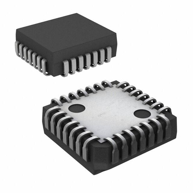
5.0 Connection Diagrams
TL/F/11085 – 16
Top View
Order Number DP8392CN
See NS Package Number N16E
TL/F/11085–6
Order Number DP8392CV
See NS Package Number V28A
FIGURE 5
4
�6.0 Pin Descriptions
16-Pin DIP
Name
I/O
Description
2
3
1
2
CD a *
CDb
O
Collision Output. Balanced differential line driver outputs from the collision detect
circuitry. The 10 MHz signal from the internal oscillator is transferred to these
outputs in the event of collision, excessive transmission (jabber), or during CD
Heartbeat condition. These outputs are open emitters; pulldown resistors to VEE
are required. When operating into a 78X transmission line, these resistors should
be 500X. In Cheapernet applications, where the 78X drop cable is not used,
higher resistor values (up to 1.5k) may be used to save power.
4
12
3
6
RX a *
RXb
O
Receive Output. Balanced differential line driver outputs from the Receiver. These
outputs also require 500X pulldown resistors.
13
14
7
8
TX a *
TXb
I
Transmit Input. Balanced differential line receiver inputs to the Transmitter. The
common mode voltage for these inputs is determined internally and must not be
externally established. Signals meeting Transmitter squelch requirements are
waveshaped and output at TXO.
15
9
HBE
I
Heartbeat Enable. This input enables CD Heartbeat when grounded, disables it
when connected to VEE.
18
19
11
12
RR a
RRb
I
External Resistor. A fixed 1k 1% resistor connected between these pins
establishes internal operating currents.
26
14
RXI
I
Receive Input. Connects directly to the coaxial cable. Signals meeting Receiver
squelch requirements are equalized for inter-symbol distortion, amplified, and
outputted at RX g .
28
15
TXO
O
Transmit Output. Connects either directly (Cheapernet) or via an isolation diode
(Ethernet) to the coaxial cable.
1
16
CDS
I
Collision Detect Sense. Ground sense connection for the collision detect circuit.
This pin should be connected separately to the shield to avoid ground drops from
altering the receive mode collision threshold.
16, 17
10
GND
et
e
28-Pin PLCC
bs
ol
Positive Supply Pin. A 0.1 mF ceramic decoupling capacitor must be connected
across GND and VEE as close to the device as possible.
5 – 11
20 – 25
4
5
13
VEE
Negative Supply Pins. In order to make full use of the 3.5W power dissipation
capability of this package, these pins should be connected to a large metal frame
area on the PC board. Doing this will reduce the operating die temperature of the
device thereby increasing the long term reliability.
*IEEE names for CD g e CI g , RX g e DI g , TX g e DO g
2. The power supply layout to the CTI should be relatively
clean. Usually the CTI’s power is supplied directly by a
DC-DC converter. The power should be routed either
through separate isolated planes, or via thick PCB traces.
For the second consideration, the packaged DP8392 must
have a thermal resistance of 40§ C –45§ C/W to meet the full
0§ C –70§ C temperature range. The CTI dissipates more
power when transmitting than while it is idle. In order to do
this the thermal resistance of the device must be 40§ C –
45§ C/W. To meet this requirement during transmission, it is
recommended that a small printed circuit board plane be
connected to all VEE pins on the solder side of the PCB.
The size of the trace plane depends on the package used
and the duty cycle of transmissions. For the DIP package
the plane should be connected to pins 4 – 5, 13, and the size
should be approximately 0.2 square inches for applications
where the duty cycle of the transmitter is very low ( k10%).
This would be typical of adapter or motherboard applications. In applications where the transmitter duty cycle may
be large (repeaters and external transceivers) the total area
should be increased to 0.4 in2. Figure 6 illustrates a recommended component side layout for these planes.
O
6.1 P.C. BOARD LAYOUT
The DP8392C package is uniquely designed to ensure that
the device meets the 1 million hour Mean Time Between
Failure (MTBF) requirement of the IEEE 802.3 standard. In
order to fully utilize this heat dissipation design, the three
VEE pins are to be connected to a copper plane which
should be included in the printed circuit board layout.
There are two basic considerations in designing a PCB for
the DP8392C and C-1 CTI. The first is ensuring that the
layout does not degrade the electrical characteristics of the
DP8392, and enables the end product to meet the IEEE
802.3 specifications. The second consideration is meeting
the thermal requirements to the DP8392.
Since the DP8392 is highly integrated the layout is actually
quite simple, and there are just a few guidelines:
1. Ensure that the parasitic capacitance added to the RXI
and TXO pins is minimized. To do this keep these signal
traces short, and remove any power planes under these
signals, and under any components that connect to these
signals. Figure 6 shows the component placement for the
DIP package. The PLCC component placement would be
similar, as shown in Figure 7 .
5
�6.0 Pin Descriptions (Continued)
For the PLCC packaged DP8392, it is recommended that a
small printed circuit board VEE plane be connected to pins
5 – 11, and a second one be connected to pins 20–25. To
reduce the thermal resistance to the required value, the
area of the plane on EACH set of pins should be t0.20 in2
for applications with low transmitter duty cycle, and t0.4 in2
for high transmit duty cycle applications. Figure 7 illustrates
a recommended component side layout for these planes.
TL/F/11085 – 14
Layout as viewed from component side
bs
ol
et
e
FIGURE 6. Typical Layout Considerations
for DP8392CN
(Not to Scale)
O
FIGURE 7. Recommended Layout and Dissipation Planes for DP8392CV (Not to Scale)
6
TL/F/11085 – 15
�7.0 Absolute Maximum Ratings (Note 1)
b 12V
Supply Voltage (VEE)
Package Power Rating at 25§ C
3.5 Watts*
(PC Board Mounted)
See Section 5
Derate linearly at the rate of 28.6 mW/§ C
Input Voltage
Storage Temperature
Lead Temp. (Soldering, 10 seconds)
Recommended Operating
Conditions
b 9v g 5%
Supply Voltage (VEE)
Ambient Temperature
0§ to 70§ C
If Military/Aerospace specified devices are required,
please contact the National Semiconductor Sales
Office/Distributors for availability and specifications.
0 to b12V
b 65§ to 150§ C
260§ C
*For actual power dissipation of the device please refer to section 7.0.
8.0 DP8392C Electrical Characteristics VEE e b9V g 5%, TA e 0§ to 70§ C (Notes 2 & 3)
All parameters with respect to CD g and RX g are measured after the pulse transformer except VOC.
Parameter
Min
Typ
Max
Units
b 85
b 130
mA
b 125
b 180
mA
Supply current out of VEE pinÐnon transmitting
IEE2
Supply current out of VEE pinÐtransmitting
IRXI
Receive input bias current (RXI)
b2
ITDC
Transmit output dc current level (TXO)
37
ITAC
Transmit output ac current level (TXO)
VCD
Collision threshold (Receive mode)
b 1.45
VOD
Differential output voltage (RX g , CD g )
g 550
VOC
Common mode output voltage (RX g , CD g )
b 1.5
VOB
Diff. output voltage imbalance (RX g , CD g )
e
Symbol
IEE1
VTS
Transmitter squelch threshold (TX g )
b 175
CX
Input capacitance (RXI)
RRXI
Shunt resistanceÐnon transmitting (RXI)
RTXO
Shunt resistanceÐtransmitting (TXO)
41
g 28
b 1.53
mA
45
mA
ITDC
mA
b 1.58
V
g 1200
mV
b 2.5
V
g 40
mV
b 300
mV
et
b 2.0
a 25
b 225
1.2
100
10
pF
KX
KX
bs
ol
9.0 DP8392C-1 Electrical Characteristics VEE e b9V g 5%, TA e 0§ to 70§ C (Notes 2 & 3)
All parameters with respect to CD g and RX g are measured after the pulse transformer except VOC.
Symbol
IEE1
IEE2
IRXI
ITDC
ITAC
VCD
VOD
VOC
VOB
VTS
Min
Supply current out of VEE pinÐtransmitting
Receive input bias current (RXI)
b2
Transmit output dc current level (TXO)
37
Transmit output ac current level (TXO)
Typ
Max
Units
b 85
b 130
mA
b 125
b 180
mA
a 25
mA
41
45
mA
ITDC
mA
b 1.53
b 1.58
V
g 1200
mV
g 28
Collision threshold (Receive mode)
b 1.45
Differential output voltage (RX g , CD g )
g 550
Common mode output voltage (RX g , CD g )
b 1.5
b 2.0
Diff. output voltage imbalance (RX g , CD g )
Transmitter squelch threshold (TX g )
b 175
Input capacitance (RXI)
b 225
1.2
O
CX
Parameter
Supply current out of VEE pinÐnon transmitting
RRXI
Shunt resistanceÐnon transmitting (RXI)
100
RTXO
Shunt resistanceÐtransmitting (TXO)
7.5K
b 2.5
V
g 40
mV
b 275
mV
pF
KX
10
KX
Note 1: Absolute maximum ratings are those values beyond which the safety of the device cannot be guaranteed. They are not meant to imply that the device
should be operated at these limits.
Note 2: All currents into device pins are positive, all currents out of device pins are negative. All voltages referenced to ground unless otherwise specified.
Note 3: All typicals are given for VEE e b 9V and TA e 25§ C.
7
�10.0 DP8392C Switching Characteristics VEE e b9V g 5%, TA e 0§ to 70§ C (Note 3)
Symbol
Parameter
Fig
Min
Typ
Max
Units
tRON
Receiver startup delay (RXI to RX g )
8 & 14
4
tRd
Receiver propagation delay (RXI to RX g )
8 & 14
15
tRr
Differential outputs rise time (RX g , CD g )
8 & 14
4
tRf
Differential outputs fall time (RX g , CD g )
8 & 14
4
ns
tRJ
Receiver & cable total jitter
13
g2
ns
tTST
Transmitter startup delay (TX g to TXO)
9 & 14
1
tTd
Transmitter propagation delay (TX g to TXO)
9 & 14
25
tTr
Transmitter rise time Ð10% to 90% (TXO)
9 & 14
25
tTf
Transmitter fall time Ð90% to 10% (TXO)
9 & 14
25
ns
tTM
tTr and tTf mismatch
0.5
ns
tTS
Transmitter skew (TXO)
g 0.5
ns
tTON
Transmit turn-on pulse width at VTS (TX g )
9 & 14
20
ns
tTOFF
Transmit turn-off pulse width at VTS (TX g )
9 & 14
250
ns
tCON
Collision turn-on delay
10 & 14
7
bits
tCOFF
Collision turn-off delay
10 & 14
fCD
Collision frequency (CD g )
10 & 14
tCP
Collision pulse width (CD g )
10 & 14
tHON
CD Heartbeat delay (TX g to CD g )
11 & 14
tHW
CD Heartbeat duration (CD g )
0.5
1.0
1.5
ms
tJA
Jabber activation delay (TX g to TXO and CD g )
12 & 14
20
29
60
ms
tJR
Jabber reset unjab time (TX g to TXO and CD g )
12 & 14
250
500
750
ms
ns
ns
bits
50
ns
ns
20
bits
12.5
MHz
e
8.0
35
70
ns
0.6
1.6
ms
et
11 & 14
bits
50
DP8392C-1 Switching Characteristics VEE e b9V g 5%, TA e 0§ to 70§ C (Note 3)
Units
Receiver startup delay (RXI to RX g )
Parameter
8 & 14
Fig
4
5
bits
tRd
Receiver propagation delay (RXI to RX g )
8 & 14
15
50
ns
tRr
Differential outputs rise time (RX g , CD g )
8 & 14
4
7
ns
tRf
Differential outputs fall time (RX g , CD g )
8 & 14
4
7
tRJ
Receiver & cable total jitter
13
g2
tTST
Transmitter startup delay (TX g to TXO)
9 & 14
1
2
bits
tTd
Transmitter propagation delay (TX g to TXO)
9 & 14
5
25
50
ns
tTr
Transmitter rise time Ð10% to 90% (TXO)
9 & 14
20
25
30
ns
tTf
Transmitter fall time Ð90% to 10% (TXO)
9 & 14
20
25
30
tTM
tTr and tTf mismatch
Min
Typ
tTS
Transmitter skew (TXO)
tTON
Transmit turn-on pulse width at VTS (TX g )
9 & 14
5
tTOFF
Transmit turn-off pulse width at VTS (TX g )
9 & 14
110
10 & 14
7
ns
ns
g 0.5
20
ns
ns
0.5
O
Symbol
bs
ol
Max
tRON
ns
40
ns
270
ns
13
bits
tCON
Collision turn-on delay
tCOFF
Collision turn-off delay
10 & 14
fCD
Collision frequency (CD g )
10 & 14
tCP
Collision pulse width (CD g )
10 & 14
35
70
ns
tHON
CD Heartbeat delay (TX g to CD g )
11 & 14
0.6
1.6
ms
tHW
CD Heartbeat duration (CD g )
11 & 14
0.5
1.0
1.5
ms
tJA
Jabber activation delay (TX g to TXO and CD g )
12 & 14
20
29
60
ms
tJR
Jabber reset unjab time (TX g to TXO and CD g )
12 & 14
250
500
750
ms
8.5
20
bits
12.5
MHz
Note 1: Absolute maximum ratings are those values beyond which the safety of the device cannot be guaranteed. They are not meant to imply that the device
should be operated at these limits.
Note 2: All currents into device pins are positive, all currents out of device pins are negative. All voltages referenced to ground unless otherwise specified.
Note 3: All typicals are given for VEE e b 9V and TA e 25§ C.
8
�11.0 Timing and Load Diagrams
TL/F/11085 – 7
e
FIGURE 8. Receiver Timing
TL/F/11085 – 8
bs
ol
et
FIGURE 9. Transmitter Timing
TL/F/11085 – 9
O
FIGURE 10. Collision Timing
TL/F/11085 – 10
FIGURE 11. Heartbeat Timing
9
�11.0 Timing and Load Diagrams (Continued)
TL/F/11085 – 11
bs
ol
et
e
FIGURE 12. Jabber Timing
Receiver equalization (jitter correction) t 1 ns
Input jitter at RX g s g 7 ns
TL/F/11085 – 12
Output jitter at RX g s g 6 ns
O
FIGURE 13. Receive Jitter Timing
TL/F/11085 – 13
*The 50 mH inductance is for testing purposes. Pulse transformers with higher inductances are recommended (see Figure 4 )
FIGURE 14. Test Loads
10
�e
12.0 Physical Dimensions inches (millimeters)
O
bs
ol
et
Molded Dual-In-Line Package (N)
Order Number DP8392CN or DP8392CN-1
NS Package Number N16E
11
�et
e
Lit. Ý103054
bs
ol
DP8392C/DP8392C-1 CTI Coaxial Transceiver Interface
12.0 Physical Dimensions inches (millimeters) (Continued)
28-Lead Plastic Chip Carrier
Order Number DP8392CV or DP8392CV-1
NS Package Number V28A
LIFE SUPPORT POLICY
O
NATIONAL’S PRODUCTS ARE NOT AUTHORIZED FOR USE AS CRITICAL COMPONENTS IN LIFE SUPPORT
DEVICES OR SYSTEMS WITHOUT THE EXPRESS WRITTEN APPROVAL OF THE PRESIDENT OF NATIONAL
SEMICONDUCTOR CORPORATION. As used herein:
1. Life support devices or systems are devices or
systems which, (a) are intended for surgical implant
into the body, or (b) support or sustain life, and whose
failure to perform, when properly used in accordance
with instructions for use provided in the labeling, can
be reasonably expected to result in a significant injury
to the user.
National Semiconductor
Corporation
1111 West Bardin Road
Arlington, TX 76017
Tel: 1(800) 272-9959
Fax: 1(800) 737-7018
2. A critical component is any component of a life
support device or system whose failure to perform can
be reasonably expected to cause the failure of the life
support device or system, or to affect its safety or
effectiveness.
National Semiconductor
Europe
Fax: (a49) 0-180-530 85 86
Email: cnjwge @ tevm2.nsc.com
Deutsch Tel: (a49) 0-180-530 85 85
English Tel: (a49) 0-180-532 78 32
Fran3ais Tel: (a49) 0-180-532 93 58
Italiano Tel: (a49) 0-180-534 16 80
National Semiconductor
Hong Kong Ltd.
13th Floor, Straight Block,
Ocean Centre, 5 Canton Rd.
Tsimshatsui, Kowloon
Hong Kong
Tel: (852) 2737-1600
Fax: (852) 2736-9960
National Semiconductor
Japan Ltd.
Tel: 81-043-299-2309
Fax: 81-043-299-2408
National does not assume any responsibility for use of any circuitry described, no circuit patent licenses are implied and National reserves the right at any time without notice to change said circuitry and specifications.
�IMPORTANT NOTICE
Texas Instruments Incorporated and its subsidiaries (TI) reserve the right to make corrections, modifications, enhancements, improvements,
and other changes to its products and services at any time and to discontinue any product or service without notice. Customers should
obtain the latest relevant information before placing orders and should verify that such information is current and complete. All products are
sold subject to TI’s terms and conditions of sale supplied at the time of order acknowledgment.
TI warrants performance of its hardware products to the specifications applicable at the time of sale in accordance with TI’s standard
warranty. Testing and other quality control techniques are used to the extent TI deems necessary to support this warranty. Except where
mandated by government requirements, testing of all parameters of each product is not necessarily performed.
TI assumes no liability for applications assistance or customer product design. Customers are responsible for their products and
applications using TI components. To minimize the risks associated with customer products and applications, customers should provide
adequate design and operating safeguards.
TI does not warrant or represent that any license, either express or implied, is granted under any TI patent right, copyright, mask work right,
or other TI intellectual property right relating to any combination, machine, or process in which TI products or services are used. Information
published by TI regarding third-party products or services does not constitute a license from TI to use such products or services or a
warranty or endorsement thereof. Use of such information may require a license from a third party under the patents or other intellectual
property of the third party, or a license from TI under the patents or other intellectual property of TI.
Reproduction of TI information in TI data books or data sheets is permissible only if reproduction is without alteration and is accompanied
by all associated warranties, conditions, limitations, and notices. Reproduction of this information with alteration is an unfair and deceptive
business practice. TI is not responsible or liable for such altered documentation. Information of third parties may be subject to additional
restrictions.
Resale of TI products or services with statements different from or beyond the parameters stated by TI for that product or service voids all
express and any implied warranties for the associated TI product or service and is an unfair and deceptive business practice. TI is not
responsible or liable for any such statements.
TI products are not authorized for use in safety-critical applications (such as life support) where a failure of the TI product would reasonably
be expected to cause severe personal injury or death, unless officers of the parties have executed an agreement specifically governing
such use. Buyers represent that they have all necessary expertise in the safety and regulatory ramifications of their applications, and
acknowledge and agree that they are solely responsible for all legal, regulatory and safety-related requirements concerning their products
and any use of TI products in such safety-critical applications, notwithstanding any applications-related information or support that may be
provided by TI. Further, Buyers must fully indemnify TI and its representatives against any damages arising out of the use of TI products in
such safety-critical applications.
TI products are neither designed nor intended for use in military/aerospace applications or environments unless the TI products are
specifically designated by TI as military-grade or "enhanced plastic." Only products designated by TI as military-grade meet military
specifications. Buyers acknowledge and agree that any such use of TI products which TI has not designated as military-grade is solely at
the Buyer's risk, and that they are solely responsible for compliance with all legal and regulatory requirements in connection with such use.
TI products are neither designed nor intended for use in automotive applications or environments unless the specific TI products are
designated by TI as compliant with ISO/TS 16949 requirements. Buyers acknowledge and agree that, if they use any non-designated
products in automotive applications, TI will not be responsible for any failure to meet such requirements.
Following are URLs where you can obtain information on other Texas Instruments products and application solutions:
Products
Applications
Audio
www.ti.com/audio
Communications and Telecom www.ti.com/communications
Amplifiers
amplifier.ti.com
Computers and Peripherals
www.ti.com/computers
Data Converters
dataconverter.ti.com
Consumer Electronics
www.ti.com/consumer-apps
DLP® Products
www.dlp.com
Energy and Lighting
www.ti.com/energy
DSP
dsp.ti.com
Industrial
www.ti.com/industrial
Clocks and Timers
www.ti.com/clocks
Medical
www.ti.com/medical
Interface
interface.ti.com
Security
www.ti.com/security
Logic
logic.ti.com
Space, Avionics and Defense
www.ti.com/space-avionics-defense
Power Mgmt
power.ti.com
Transportation and Automotive www.ti.com/automotive
Microcontrollers
microcontroller.ti.com
Video and Imaging
RFID
www.ti-rfid.com
OMAP Mobile Processors
www.ti.com/omap
Wireless Connectivity
www.ti.com/wirelessconnectivity
TI E2E Community Home Page
www.ti.com/video
e2e.ti.com
Mailing Address: Texas Instruments, Post Office Box 655303, Dallas, Texas 75265
Copyright © 2011, Texas Instruments Incorporated
�


 工商网监
湘ICP备2023018690号
工商网监
湘ICP备2023018690号
