Product
Folder
Sample &
Buy
Support &
Community
Tools &
Software
Technical
Documents
Reference
Design
DRV10963
SLAS955A – MARCH 2013 – REVISED JULY 2015
DRV10963 5-V, Three-Phase, Sensorless BLDC Motor Driver
1 Features
3 Description
•
The DRV10963 is a three phase sensor-less motor
driver with integrated power MOSFETs. It is
specifically designed for high efficiency, low noise
and low external component count motor drive
applications. The proprietary sensor-less window-less
180° sinusoidal control scheme offers ultra-quiet
motor drive performance. The DRV10963 contains an
intelligent lock detect function, combined with other
internal protection circuits to ensure safe operation.
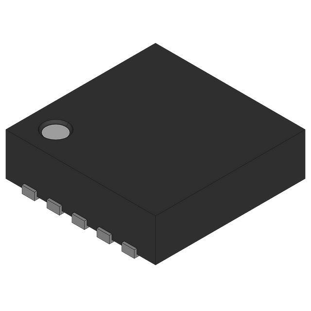
The DRV10963 is available in a thermally efficient 10pin USON package with an exposed thermal pad.
1
•
•
•
•
•
•
•
•
•
Proprietary Sensor-less Window-less
180° Sinusoidal Control Scheme
Input Voltage Range 2.1 to 5.5 V
500-mA Output Current
Low Quiescent Current 15 µA (Typical) at Sleep
Mode
Total Driver H+L Rdson Less than 1.5 Ω
Current Limit and Short Circuit Current Protection
Lock Detection
Anti Voltage Surge (AVS)
UVLO
Thermal Shutdown
Device Information
PART NUMBER
DRV10963
BODY SIZE (NOM)
3.00 mm × 3.00 mm
(1) For all available packages, see the orderable addendum at
the end of the data sheet.
2 Applications
•
•
•
PACKAGE
USON (10)
Notebook CPU Fans
Game Station CPU Fans
ASIC Cooling Fans
Simplified Schematic
Vcc
100k
FG
1 FG
2 FGS
Vcc
3 VCC
4 W
2.2uF
Gnd
PWM 10
GND 9
FR 8
PWMIN
U 7
5 GND
V
6
Gnd
M
1
An IMPORTANT NOTICE at the end of this data sheet addresses availability, warranty, changes, use in safety-critical applications,
intellectual property matters and other important disclaimers. PRODUCTION DATA.
�DRV10963
SLAS955A – MARCH 2013 – REVISED JULY 2015
www.ti.com
Table of Contents
1
2
3
4
5
6
7
Features ..................................................................
Applications ...........................................................
Description .............................................................
Revision History.....................................................
Pin Configuration and Functions .........................
Specifications.........................................................
1
1
1
2
3
4
6.1
6.2
6.3
6.4
6.5
6.6
4
4
4
4
5
6
Absolute Maximum Ratings ......................................
ESD Ratings..............................................................
Recommended Operating Conditions.......................
Thermal Information ..................................................
Electrical Characteristics...........................................
Typical Characteristics ..............................................
Detailed Description .............................................. 7
7.1 Overview ................................................................... 7
7.2 Functional Block Diagram ......................................... 7
7.3 Feature Description................................................... 8
7.4 Device Functional Modes........................................ 17
8
Application and Implementation ........................ 19
8.1 Application Information............................................ 19
8.2 Typical Application .................................................. 19
9 Power Supply Recommendations...................... 22
10 Layout................................................................... 22
10.1 Layout Guidelines ................................................. 22
10.2 Layout Example .................................................... 22
11 Device and Documentation Support ................. 23
11.1
11.2
11.3
11.4
Community Resources..........................................
Trademarks ...........................................................
Electrostatic Discharge Caution ............................
Glossary ................................................................
23
23
23
23
12 Mechanical, Packaging, and Orderable
Information ........................................................... 23
4 Revision History
NOTE: Page numbers for previous revisions may differ from page numbers in the current version.
Changes from Original (March 2013) to Revision A
•
2
Page
Added ESD Ratings table, Feature Description section, Device Functional Modes, Application and Implementation
section, Power Supply Recommendations section, Layout section, Device and Documentation Support section, and
Mechanical, Packaging, and Orderable Information section ................................................................................................. 1
Submit Documentation Feedback
Copyright © 2013–2015, Texas Instruments Incorporated
Product Folder Links: DRV10963
�DRV10963
www.ti.com
SLAS955A – MARCH 2013 – REVISED JULY 2015
5 Pin Configuration and Functions
DSN Package
10-Pin USON
Top View
FG
1
10
PWM
FGS
2
9
GND
VCC
3
8
FR
W
4
7
U
GND
5
6
V
Pin Functions
PIN
NUMBER
NAME
I/O
DESCRIPTION
1
FG
Output
2
FGS
Input
3
VCC
Power
4
W
IO
5
GND
Ground
6
V
IO
Motor Phase V
7
U
IO
Motor Phase U
8
FR
Input
9
GND
Ground
10
PWM
Input
—
Thermal
Pad
—
Motor speed indicator output (open drain)
Motor speed indicator selector. The state of this pin is latched on power up and can not be changed
dynamically.
Input voltage for motor and chip supply
Motor Phase W
Ground
Motor direction selector. This pin can be dynamically changed after power up.
Ground
Motor speed control input.
Connect to Ground for maximum thermal efficiency. Thermal pad is on the bottom of the package
Submit Documentation Feedback
Copyright © 2013–2015, Texas Instruments Incorporated
Product Folder Links: DRV10963
3
�DRV10963
SLAS955A – MARCH 2013 – REVISED JULY 2015
www.ti.com
6 Specifications
6.1 Absolute Maximum Ratings
over operating free-air temperature range (unless otherwise noted) (1)
(2)
VCC Pin supply voltage
MIN
MAX
UNIT
–0.3
6
V
Motor phase pins (U, V, W)
–1
7.7
V
Direction, speed indicator input, and speed input (FR, FGS, PWM)
–0.3
6
V
Speed output (FG)
–0.3
7.7
V
TJ
Junction temperature
–40
150
°C
TSDR
Maximum lead soldering temperature, 10 seconds
260
°C
Tstg
Storage temperature
150
°C
(1)
(2)
–55
Stresses beyond those listed under Absolute Maximum Ratings may cause permanent damage to the device. These are stress ratings
only, which do not imply functional operation of the device at these or any other conditions beyond those indicated under Recommended
Operating Conditions. Exposure to absolute-maximum-rated conditions for extended periods may affect device reliability.
All voltages are with respect to ground.
6.2 ESD Ratings
VALUE
Human-body model (HBM), per ANSI/ESDA/JEDEC JS-001
V(ESD)
(1)
(2)
Electrostatic discharge
(1)
UNIT
±3000
Charged-device model (CDM), per JEDEC specification JESD22C101 (2)
V
±1500
JEDEC document JEP155 states that 500-V HBM allows safe manufacturing with a standard ESD control process.
JEDEC document JEP157 states that 250-V CDM allows safe manufacturing with a standard ESD control process.
6.3 Recommended Operating Conditions
over operating free-air temperature range (unless otherwise noted)
MIN
MAX
2.1
5.5
UNIT
V
–0.1
7
V
–0.1
5.5
VCC
VCC Pin supply voltage
U, V, W
Motor phase pins
FR, FGS,
PWM
Direction, speed indicator input, and speed input
FG
Speed output
–0.1
7.5
V
TJ
Junction temperature
–40
125
°C
V
6.4 Thermal Information
DRV10963
THERMAL METRIC (1)
DSN (USON)
UNIT
10 PINS
RθJA
Junction-to-ambient thermal resistance
40.9
°C/W
RθJC(top)
Junction-to-case (top) thermal resistance
46.6
°C/W
RθJB
Junction-to-board thermal resistance
15.8
°C/W
ψJT
Junction-to-top characterization parameter
0.5
°C/W
ψJB
Junction-to-board characterization parameter
16
°C/W
RθJC(bot)
Junction-to-case (bottom) thermal resistance
2.9
°C/W
(1)
4
For more information about traditional and new thermal metrics, see the Semiconductor and IC Package Thermal Metrics application
report, SPRA953.
Submit Documentation Feedback
Copyright © 2013–2015, Texas Instruments Incorporated
Product Folder Links: DRV10963
�DRV10963
www.ti.com
SLAS955A – MARCH 2013 – REVISED JULY 2015
6.5 Electrical Characteristics
(VCC = 5 V, TA = 25°C unless otherwise noted)
PARAMETER
TEST CONDITION
MIN
TYP
MAX
UNIT
SUPPLY CURRENT
IVCC
Operating current
PWM = VCC, no motor connected
5.5
IVCC_SLEEP
Sleep current
PWM = 0 V
15
20
mA
µA
2
2.1
V
UVLO
VUVLO_H
Undervoltage threshold high
VUVLO_L
Undervoltage threshold low
1.7
1.8
VUVLO_HYS
Undervoltage threshold hysteresis
100
200
300
mV
1
1.5
Ω
V
INTEGRATED MOSFET
RDSON
Series resistance (H+L)
VCC = 5 V; IOUT = 0.5 A
PWM
VIH_PWM
Input high threshold
VIL_PWM
Input low threshold
2.3
FPWM
PWM input frequency
RPU_PWM_VCC
PWM pin pullup resistor
TSLEEP
Sleep entry time
PWM = 0 V
IOL_FG
FG sink current
VFG = 0.3 V
ISC_FG
FG short circuit current
VFG = 5 V
Duty cycle >0% and minimum
operation duty cycle. The minimum operation duty cycle can be set to either 13%, 10%, 5% or no limit by OTP
setting (MINOP_DC[1:0]). Table 1 shows the optional settings for the minimum operation duty cycle. When the
PWM commanded duty cycle is lower than minimum operation duty cycle and higher than 1.5%, the output will
be controlled at the minimum operation duty cycle. When the input duty cycle is lower than 1.5%, the DRV10963
device will not drive the output, and enters the standby mode. This is illustrated in Figure 6.
Table 1. Minimum Operation Duty Cycle
MINOP_DC[1:0]
MINIMUM OPERATION DUTY
CYCLE
0
0 (no limit)
1
5%
2
10%
3
13%
Output Average Amplitude
Output Duty
90%
VCC
13%VCC
10%VCC
10%
5%VCC
0 5% 10%
13%
1.5%
Input Duty
Optional Transfer Functions:
(13%, 10%, 5%, no limit)
0
10%
Input Duty
Example: Minimum Duty Cycle = 10%
Figure 6. Speed Control Transfer Function
7.3.2 Spin up Settings
DRV10963 starts the motor using a procedure which is illustrated in Figure 7.
The motor start profile includes device configurable options for open loop to close loop transition threshold
(HOffth), align time (TAlign), and accelerate rate (RAcc).
Submit Documentation Feedback
Copyright © 2013–2015, Texas Instruments Incorporated
Product Folder Links: DRV10963
9
�DRV10963
SLAS955A – MARCH 2013 – REVISED JULY 2015
www.ti.com
To align the rotor to the commutation logic the DRV10963 applies an x% duty cycle on phases V and W while
holding phase U at GND. This condition is maintained for TAlign seconds. The x% value is determined by the
VCC voltage (as shown in Table 2) to maintain sufficient driving torque over a wide range of supply voltages.
Power On
Calibration
Align
300 ms
Resistance
Measurement
Open Loop
Accelerate
Wait TOFF_LOCK
Coasting
Lock Detected
Kt
Measurement
Close Loop
Closed Loop
Figure 7. DRV10963 Initialization and Motor Start-up Sequence
Table 2. Align and Open Loop Duty Cycle
VCC VOLTAGE
DUTY CYCLE DURING ALIGN
AND OPEN LOOP (X)%
5.25 to approximately 6 V
43%
4.5 to approximately 5.25 V
50%
3.75 to approximately 4.5 V
60%
3 to approximately 3.75 V
75%
V->W
U->W->V
7.3.4 Motor Frequency Feedback (FG)
During operation of the DRV10963 device, the FG pin provides an indication of the speed of the motor. The
output provided on this pin can be configured by use of an OTP setting (FGOPT) and by applying a logic signal
to the FGS pin. The configuration of this output is defined in Table 6.
Table 6. FG Motor Status Speed Indicator Configuration
MOTOR CONDITION
DRV10963xxDSNR Normal
Operation
(FGS = 1)
FGOPT=1,(FGS = 0)
FGOPT=0,(FGS = 0)
Toggles once per electrical cycle
Toggles once every 2
electrical cycles
Toggles once every 3
electrical cycles
As seen in Table 6, the FG pin can be configured to toggle either once per electrical cycle, once per 2 electrical
cycles or once per every 3 electrical cycles. Using this information and the number of pole pairs in the motor, the
mechanical speed of the motor can be determined.
The formula to determine the speed of the motor is:
If FGS = 1, RPM = (FREQFG × 60)/ number of pole pairs
If FGS = 0, FGOPT=1, RPM = (FREQFG × 120)/ number of pole pairs
(2)
(3)
If FGS = 0, FGOPT=0, RPM = (FREQFG × 180)/ number of pole pairs
(4)
or
The FG pin has built in short circuit protection, which limits the current in the event that the pin is shorted to VCC.
The current will be limited to ISC_FG.
7.3.5 Lock Detection
When the motor is locked by some external condition the DRV10963 will detect the lock condition and will take
action to protect the motor and the device. The lock condition must be properly detected whether it occurs as a
result of a slowly increasing load or a sudden shock.
The DRV10963 reacts to lock conditions by stopping the motor drive. To stop driving the motor the phase
outputs are placed into a high impedance state. To prevent the current which is flowing in the motor from being
returned to the power supply (VCC) the DRV10963 uses an ANTI VOLTAGE SURGE feature. This feature is
described in a following section. After successfully transitioning into a high impedance state as the result of a
lock condition the DRV10963 will attempt to restart the motor after TOFF_LOCK seconds.
The DRV10963 has a comprehensive lock detect function which includes 5 different lock detect schemes. Each
of these schemes detects a particular condition of lock as illustrated in Figure 9.
Frequency Overflow
Bemf Abnormal
Speed Abnormal
Or
Tri-state
and Restart
Logic
Closed Loop Stuck
Open Loop Stuck
Figure 9. Lock Detect
The behavior of each lock detect scheme is described in the following sections.
12
Submit Documentation Feedback
Copyright © 2013–2015, Texas Instruments Incorporated
Product Folder Links: DRV10963
�DRV10963
www.ti.com
SLAS955A – MARCH 2013 – REVISED JULY 2015
7.3.5.1 Lock1: Frequency Overflow
For most applications the maximum electrical frequency of the motor will be less than 3 kHz. If the motor is
stopped then the BEMF voltage will be zero. Under this condition, when the DRV10963 device is in the closed
loop mode, the sensor less control algorithm will continue to accelerate the electrical commutation rate even
though the motor is not spinning. A lock condition is triggered if the electrical frequency exceeds 3 kHz.
7.3.5.2 Lock2: BEMF Abnormal
For any specific motor, the integrated value of BEMF during half of an electronic cycle will be a constant as
illustrated by the shaded green area in Figure 10. This is true regardless of whether the motor runs fast or slow.
The DRV10963 monitors this value and uses it as a criterion to determine if the motor is in a lock condition.
The DRV10963 uses the integrated BEMF to determine the Kt value of the motor during the initial motor start.
Based on this measurement a range of acceptable Kt values is established. This range is referred to as Kt_low
and Kt_high. During closed loop motor operation the Ktc value is continuously updated. If the calculated Ktc goes
beyond the acceptable range a lock condition is triggered. This is illustrated in Figure 11.
Figure 10. BEMF Integration
Figure 11. Abnormal Kt Lock Detect
7.3.5.3 Lock3: Speed Abnormal
If the motor is in normal operation the motor BEMF will always be less than the voltage applied to the phase. The
DRV10963 sensorless control algorithm is continuously updating the value of the motor BEMF based on the
speed of the motor and the motor Kt as shown in Figure 12. If the calculated value for motor BEMF is higher than
the applied voltage (U) for a certain period of time (TON_LOCK) then there is an error in the system. The
calculated value for motor BEMF is wrong or the motor is out of phase with the commutation logic. When this
condition is detected a lock detect is triggered.
Figure 12. BEMF Monitoring
Submit Documentation Feedback
Copyright © 2013–2015, Texas Instruments Incorporated
Product Folder Links: DRV10963
13
�DRV10963
SLAS955A – MARCH 2013 – REVISED JULY 2015
www.ti.com
7.3.5.4 Open Loop Stuck
This lock condition is active when the DRV10963 device is operating in the open loop mode. When the open loop
commutation rate becomes higher than the open to closed loop threshold (HOffth - see Figure 8) and the zero
cross is not detected for the time corresponding to 2 electrical cycles then this is an indication that the motor is
not moving. Under this condition the open loop stuck lock condition will be triggered.
7.3.6 Soft Current Limit
The current limit function provides active protection for preventing damage as a result of high current. The soft
current limit does not use direct current measurement for protection, but rather, uses the measured motor
resistance (Rm) and motor velocity constant (Kt) to limit the voltage applied to the phase (U) such that the
current does not exceed the limit value (ILIMIT). This is illustrated in Figure 13 based on the calculation shown in
Equation 5.
The soft limit is only active when in normal closed loop mode and does not result in a fault condition nor does it
result in the motor being stopped. The soft current limit is typically useful for limiting the current that results from
heavy loading during motor acceleration.
Figure 13. Current Limit
ULIMIT=ILIMIT × R_m + Speed × Kt
(5)
ILIMIT is configured by OTP setting (ILIMIT [2:0]) according to Table 7.
NOTE
The soft current limit calculation is not correct if the motor is out of phase with the
commutation control logic (locked rotor). The soft current limit will not be effective under
this condition.
Table 7. ILIMIT Settings
ILIMIT [2:0]
ILIMIT
0
No current limit
1
125 mA
2
250 mA
3
375 mA
4
500 mA
5
625 mA
6
750 mA
7
875 mA
7.3.7 Short Circuit Current Protection
The short circuit current protection function shuts off drive to the motor by placing the motor phases into a high
impedance state if the current in any motor phase exceeds the short circuit protection limit ISHT. The DRV10963
device will go through the initialization sequence and will attempt to restart the motor after the short circuit
condition is removed. This function is intended to protect the device and the motor from catastrophic failure when
subjected to a short circuit condition.
14
Submit Documentation Feedback
Copyright © 2013–2015, Texas Instruments Incorporated
Product Folder Links: DRV10963
�DRV10963
www.ti.com
SLAS955A – MARCH 2013 – REVISED JULY 2015
7.3.8 Anti-Voltage Surge (AVS)
Under normal operation the DRV10963 acts to transfer energy from the power supply to the motor to generate
torque, which results in angular rotation of the motor. Under certain conditions, however, energy which is stored
in the motor in the form of inductive energy or angular momentum (mechanical energy) can be returned to the
power supply. This can happen whenever the output voltage is quickly interrupted or whenever the voltage
applied to the motor becomes less than the BEMF voltage generated by the motor. The energy which is returned
to the supply can cause the supply voltage to increase. This condition is referred to as voltage surge.
The DRV10963 includes an anti-voltage-surge (AVS) feature which prevents energy from being transferred from
the motor to the power supply. This feature helps to protect the DRV10963 as well as any other components that
are connected to the power supply (VCC).
7.3.8.1 Protecting Against the Return of Mechanical Energy
Mechanical energy is typically returned to the power supply when the speed command is abruptly decreased. If
the voltage applied to the phase becomes less than the BEMF voltage then the motor will work as a generator
and current will flow from the motor back to VCC. This is illustrated in Figure 14. To prevent this from happening,
the DRV10963 buffers the speed command value and limits the rate at which it is able to change. The AVS
function acts to ensure that the effective output amplitude (U) is maintained to be larger than the BEMF voltage.
This prevents current from becoming less than zero. The value of BEMF used to perform this function is
calculated by the motor Kt and the motor speed.
Figure 14. Mechanical AVS
7.3.8.2 Protecting Against the Return of Inductive Energy
When the DRV10963 suddenly stops driving the motor, the current which is flowing in the motor’s inductance will
continue to flow. It flows through the intrinsic body diodes in the mosfets and charges VCC. An example of this
behavior is illustrated by the two pictures in the top half of Figure 15. When the driver is active, the current flows
from S1 to the motor and then to S6 and is returned to ground. When the driver is placed into a high impedance
(tri-state) mode, the current goes flows from ground through the body diode of S2 to the motor and then through
the body diode of S5 to VCC. The current will continue to flow through the motor’s inductance in this direction
until the inductive energy is dissipated.
Figure 15. Inductive AVS
Submit Documentation Feedback
Copyright © 2013–2015, Texas Instruments Incorporated
Product Folder Links: DRV10963
15
�DRV10963
SLAS955A – MARCH 2013 – REVISED JULY 2015
www.ti.com
The lower two pictures in Figure 14 illustrate how the AVS circuit in the DRV10963 device prevents this energy
from being returned to the supply. When the AVS condition is detected the DRV10963 device will act to turn on
the low side device designated as S6. This allows the current flowing in the motor inductance to be returned to
ground instead of being directed to the VCC supply voltage.
7.3.9 Control Advance Angle
To achieve the best efficiency it is often desirable to control the drive state of the motor so that the motor’s phase
current is aligned with the motor’s BEMF voltage.
To align the motor’s phase current with the motor’s BEMF voltage the inductive effect of the motor must be
considered. The voltage applied to the motor should be applied in advance of the motor’s BEMF voltage. This is
illustrated in Figure 16. The DRV10963 provides configuration bits (CTRL_ANG[4:0] )for controlling the time
(Tadv) between the driving voltage and BEMF. For motors with salient pole structures, aligning the motor BEMF
voltage with the motor current may not achieve the best efficiency. In these applications the timing advance
should be adjusted accordingly. This can be accomplished by operating the system at constant speed and load
conditions and by adjusting the Tadv until the minimum current is achieved.
Figure 16. DRV10963 Advance Angle Control
Table 8. Control Advance Angle Settings
CTRL_ANG[4:0]
Tadv
0
0
1
20 µs
2
40 µs
3
60 µs
n
n × 20 µs
6
120 µs
8
160 µs
31
620 µs
7.3.10 Overtemperature Protection
The DRV10963 contains a thermal shut down function which disables motor operation when the device junction
temperature has exceeded TSD. Motor operation will resume when the junction temperature becomes lower than
TSD - TSD_HYS.
7.3.11 Undervoltage Protection
The DRV10963 contains an undervoltage lockout feature, which prevents motor operation whenever the supply
voltage (VCC) becomes too low. Upon power up, the DRV10963 will operate once VCC rises above VUVLO_H.
The DRV10963 will continue to operate until VCC falls below VUVLO_L.
7.3.12 OTP Configuration
The DRV10963 features OTP (one time programmable) bits to allow for flexible configuration of the device in
order for optimization over a wide range of applications. Selection of various OTP options is described
throughout this specification. The DRV10963JJ, DRV10963JM, DRV10963JU, and DRV10963JA parts listed in
Table 10 are configured at the factory based on popular OTP settings for several different applications. TI
provides EVM hardware along with a special GUI and a Motor System Tuning Guide which provides detailed
instructions for determining the right part for your application. If your application requires settings not provided in
16
Submit Documentation Feedback
Copyright © 2013–2015, Texas Instruments Incorporated
Product Folder Links: DRV10963
�DRV10963
www.ti.com
SLAS955A – MARCH 2013 – REVISED JULY 2015
any of the DRV10963Jx parts then the DRV10963P part can be used. The DRV10963P part provides blank OTP
settings that can be configured for optimal performance in your application. The TI provided EVM and GUI will
allow you to configure the OTP settings. Consult your TI representative if your application requires settings that
are not available in the DRV10963Jx configurations described and if you are unable to use the DRV10963P
option. The OTP bits used to configure the various part revisions are shown for reference in Table 10.
Table 9. OTP Configuration Bits
OTP BIT NAMES
DESCRIPTION
REFERENCE TO
MINOP_DC[1:0]
Minimum
operational duty
cycle
Figure 6
SLEEP_EN
Sleep mode enable
Standby Mode and Sleep
Mode
TARA_TH[3:0]
Start-up time and
accelerate setting
Spin up Settings
HO_TH[3:0]
Openloop to closed
loop threshold.
Spin up Settings
ILIMIT[2:0]
Current limit
setting.
Table 7
CTRL_ANG[4:0]
Control advance
angle.
Table 8
FGOPT
FG output option.
Motor Frequency Feedback
(FG)
Table 10. The OTP Setting of the Factory Configured Parts
MINOP_DC
[1:0]
SLEEP_EN
TARA_TH [3:0]
HO_TH [3:0]
ILIMIT [2:0]
CTRL_ANG
[4:0]
FGOPT
DRV10963JJ
2
1
7
8
4
6
0
DRV10963JM
2
1
E
4
4
6
1
DRV10963JU
2
1
C
7
4
6
0
DRV10963JA
2
1
7
8
4
8
0
DRV10963P
0
0
0
0
0
0
0
7.4 Device Functional Modes
7.4.1 Standby Mode and Sleep Mode
When the PWM commanded duty cycle input is lower than 1.5%, the phase outputs will be put into a high
impedance state. The device will stop driving the motor. The device logic is still active during standby mode and
the DRV10963 device will consume current as specified by IVCC.
When the PWM commanded duty cycle input is driven to 0% (less than VIL_PWM for at least TSLEEP time), the
DRV10963 device will enter a low power sleep mode. In sleep mode, most of the circuitry in the device will be
disabled to minimize the system current. The current consumption in this state is specified by IVCC_SLEEP.
The device will remain in sleep mode until either the PWM commanded duty cycle input is driven to a logic high
(higher than VIH_PWM) or the PWM input pin is allowed to float. If the input is allowed to float an internal pullup
resistor will raise the voltage to a logic high level.
Recovering from sleep mode is treated the same as power on condition as illustrated in Figure 7.
As part of the device initialization the motor resistance value and the motor Kt value are measured during the
initial motor spin up as shown in Figure 7. Whenever the part is executing the initialization sequence it is
important to note that the values determined by any previous spin up cycles no longer exist. In order for the
motor resistance value and the motor Kt value to be properly initialized the system should be allowed to come to
a complete stop before the next restart attempt.
Submit Documentation Feedback
Copyright © 2013–2015, Texas Instruments Incorporated
Product Folder Links: DRV10963
17
�DRV10963
SLAS955A – MARCH 2013 – REVISED JULY 2015
www.ti.com
Device Functional Modes (continued)
Sleep mode can be disabled by OTP setting (SLEEP_EN). In this condition, the motor resistance value and the
motor Kt value are preserved and the motor can reliably spin up without coming to a complete stop. This feature
is referred to as the ‘re-synchronize’ function. If the ‘re-synchronize’ function is required the sleep mode cannot
be used.
18
Submit Documentation Feedback
Copyright © 2013–2015, Texas Instruments Incorporated
Product Folder Links: DRV10963
�DRV10963
www.ti.com
SLAS955A – MARCH 2013 – REVISED JULY 2015
8 Application and Implementation
NOTE
Information in the following applications sections is not part of the TI component
specification, and TI does not warrant its accuracy or completeness. TI’s customers are
responsible for determining suitability of components for their purposes. Customers should
validate and test their design implementation to confirm system functionality.
8.1 Application Information
DRV10963 is used in sensorless 3-phase BLDC motor control. The driver provides a high performance, high
reliability, flexible and simple solution for compute fan applications. The following design shows a common
application of the DRV10963.
8.2 Typical Application
Vcc
100k
FG
1 FG
2 FGS
Vcc
3 VCC
4 W
2.2uF
PWM 10
GND 9
FR 8
U 7
5 GND
Gnd
PWMIN
V
Gnd
6
M
Figure 17. Typical Application Schematic
8.2.1 Design Requirements
Table 11 lists several key motor characteristics and recommended ranges which the DRV10963 is capable of
driving. However, that does not necessarily mean motors outside these boundaries cannot be driven by
DRV10963.
Recommended ranges listed in Table 11 can serve as a general guideline to quickly decide whether DRV10963
is a good fit for an application. Motor performance is not ensured for all uses.
Table 11. Key Motor Characteristics and Recommended Ranges
Recommended
Value
Rm (Ω)
Lm (µH)
Kt (mV/Hz)
fFG_max (Hz)
2.5 ~ 36
50 ~ 10000
1 ~ 100
1300
Submit Documentation Feedback
Copyright © 2013–2015, Texas Instruments Incorporated
Product Folder Links: DRV10963
19
�DRV10963
SLAS955A – MARCH 2013 – REVISED JULY 2015
www.ti.com
Rm - Motor phase resistance between phase to phase;
Lm - Motor phase to phase inductance between phase to phase;
Kt - Motor BEMF constant from phase to center tape;
fFG_max - Maximum electrical frequency. Maximum motor speed can be calculated from:
• If FGS = 1, RPM = (fFG_max × 60)/ number of pole pairs
• If FGS = 0, RPM = (fFG_max × 120)/ number of pole pairs
8.2.2 Detailed Design Procedure
1. Refer to Design Requirements and make sure your system meets the recommended application range.
2. Refer to the DRV10963 Tuning Guide and measure the motor parameters.
3. Refer to the DRV10963 Tuning Guide. Configure the parameters using DRV10963 GUI, and optimize the
motor operation. The Tuning Guide takes the user through all the configurations step by step, including: start-up
operation, closed-loop operation, current control, initial positioning, lock detection, and anti-voltage surge.
4. Build your hardware based on Layout Guidelines.
5. Connect the device into system and validate your system solution
8.2.3 Application Curves
NOTE: FG_OUT Signal Being Held HIGH During Locked Rotor
Condition (Stall)
Figure 18. Reference PCB Sinusoidal Current Profile
20
Figure 19. Reference PCB Start-Up (Align-Acceleration)
Profile
Submit Documentation Feedback
Copyright © 2013–2015, Texas Instruments Incorporated
Product Folder Links: DRV10963
�DRV10963
www.ti.com
SLAS955A – MARCH 2013 – REVISED JULY 2015
Figure 20. Reference PCB Open Loop and Close Loop
Figure 21. Reference PCB Closed Loop
Submit Documentation Feedback
Copyright © 2013–2015, Texas Instruments Incorporated
Product Folder Links: DRV10963
21
�DRV10963
SLAS955A – MARCH 2013 – REVISED JULY 2015
www.ti.com
9 Power Supply Recommendations
The DRV10963 is designed to operate from an input voltage supply, V(VCC), range from 2.1 and 5.5 V. The user
must place a 2.2-μF ceramic capacitor rated for VCC as close as possible to the VCC and GND pin.
10 Layout
10.1 Layout Guidelines
The package uses an exposed pad to remove heat from the device. For proper operation, this pad must be
thermally connected to copper on the PCB to dissipate heat. On a multi-layer PCB with a ground plane, this can
be accomplished by adding a number of vias to connect the thermal pad to the ground plane. On PCBs without
internal planes, copper area can be added on either side of the PCB to dissipate heat. If the copper area is on
the opposite side of the PCB from the device, thermal vias are used to transfer the heat between top and bottom
layers.
For details about how to design the PCB, refer to TI application report, PowerPAD™ Thermally Enhanced
Package (SLMA002), and TI application brief, PowerPAD™ Made Easy (SLMA004), available at www.ti.com. In
general, the more copper area that can be provided, the more power can be dissipated.
10.2 Layout Example
2.2uF
GND
VCC
100k
PWM
FG
1
10
FGS
2
9
GND
8
FR
100k
GND
(PPAD)
VCC
3
W
4
7
U
GND
5
6
V
Figure 22. DRV10963 Layout Example
22
Submit Documentation Feedback
Copyright © 2013–2015, Texas Instruments Incorporated
Product Folder Links: DRV10963
�DRV10963
www.ti.com
SLAS955A – MARCH 2013 – REVISED JULY 2015
11 Device and Documentation Support
11.1 Community Resources
The following links connect to TI community resources. Linked contents are provided "AS IS" by the respective
contributors. They do not constitute TI specifications and do not necessarily reflect TI's views; see TI's Terms of
Use.
TI E2E™ Online Community TI's Engineer-to-Engineer (E2E) Community. Created to foster collaboration
among engineers. At e2e.ti.com, you can ask questions, share knowledge, explore ideas and help
solve problems with fellow engineers.
Design Support TI's Design Support Quickly find helpful E2E forums along with design support tools and
contact information for technical support.
11.2 Trademarks
E2E is a trademark of Texas Instruments.
All other trademarks are the property of their respective owners.
11.3 Electrostatic Discharge Caution
These devices have limited built-in ESD protection. The leads should be shorted together or the device placed in conductive foam
during storage or handling to prevent electrostatic damage to the MOS gates.
11.4 Glossary
SLYZ022 — TI Glossary.
This glossary lists and explains terms, acronyms, and definitions.
12 Mechanical, Packaging, and Orderable Information
The following pages include mechanical packaging and orderable information. This information is the most
current data available for the designated devices. This data is subject to change without notice and revision of
this document. For browser-based versions of this data sheet, refer to the left-hand navigation.
Submit Documentation Feedback
Copyright © 2013–2015, Texas Instruments Incorporated
Product Folder Links: DRV10963
23
�PACKAGE OPTION ADDENDUM
www.ti.com
10-Dec-2020
PACKAGING INFORMATION
Orderable Device
Status
(1)
Package Type Package Pins Package
Drawing
Qty
Eco Plan
(2)
Lead finish/
Ball material
MSL Peak Temp
Op Temp (°C)
Device Marking
(3)
(4/5)
(6)
DRV10963DSNR
ACTIVE
SON
DSN
10
3000
RoHS & Green
NIPDAU
Level-2-260C-1 YEAR
-40 to 125
10963B
DRV10963JJDSNT
ACTIVE
SON
DSN
10
250
RoHS & Green
NIPDAU
Level-2-260C-1 YEAR
-40 to 125
963JJ
DRV10963JUDSNR
ACTIVE
SON
DSN
10
3000
RoHS & Green
NIPDAU
Level-2-260C-1 YEAR
-40 to 125
963JU
(1)
The marketing status values are defined as follows:
ACTIVE: Product device recommended for new designs.
LIFEBUY: TI has announced that the device will be discontinued, and a lifetime-buy period is in effect.
NRND: Not recommended for new designs. Device is in production to support existing customers, but TI does not recommend using this part in a new design.
PREVIEW: Device has been announced but is not in production. Samples may or may not be available.
OBSOLETE: TI has discontinued the production of the device.
(2)
RoHS: TI defines "RoHS" to mean semiconductor products that are compliant with the current EU RoHS requirements for all 10 RoHS substances, including the requirement that RoHS substance
do not exceed 0.1% by weight in homogeneous materials. Where designed to be soldered at high temperatures, "RoHS" products are suitable for use in specified lead-free processes. TI may
reference these types of products as "Pb-Free".
RoHS Exempt: TI defines "RoHS Exempt" to mean products that contain lead but are compliant with EU RoHS pursuant to a specific EU RoHS exemption.
Green: TI defines "Green" to mean the content of Chlorine (Cl) and Bromine (Br) based flame retardants meet JS709B low halogen requirements of


 工商网监
湘ICP备2023018690号
工商网监
湘ICP备2023018690号
