Sample &
Buy
Product
Folder
Support &
Community
Tools &
Software
Technical
Documents
DRV2700
SLOS861B – MARCH 2015 – REVISED APRIL 2015
DRV2700 Industrial Piezo Driver With Integrated Boost Converter
1 Features
3 Description
•
•
The DRV2700 device is a single-chip piezo driver
with an integrated 105-V boost switch, integrated
power diode, and integrated fully-differential amplifier.
This versatile device is capable of driving both highvoltage and low-voltage piezoelectric loads. The input
signal can be either differential or single-ended and
AC or DC coupled. The DRV2700 device supports
four GPIO-controlled gains: 28.8 dB, 34.8 dB, 38.4
dB, and 40.7 dB.
1
•
•
•
•
•
•
•
100-V Boost or 1-kV Flyback Configuration
±100-V Piezo Driver in Boost + Amplifier
Configuration
– 4 GPIO-Adjustable Gains
– Differential or Single-Ended Output
– Low-Voltage Control
– AC and DC Output Control
0 to 1-kV Piezo Driver in Flyback Configuration
– Low-Voltage Control
– AC and DC Output Control
Integrated Boost or Flyback Converter
– Adjustable Current-Limit
– Integrated Power FET and Diode
Fast Startup Time of 1.5 ms
Wide Supply-Voltage Range of 3 to 5.5 V
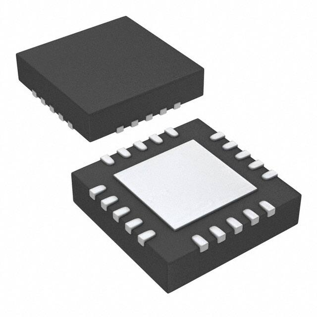
4-mm × 4-mm × 0.9-mm VQFN package
1.8-V Compatible Digital Pins
Thermal Protection
The boost voltage is set using two external resistors.
The boost current-limit is programmable through the
R(REXT) resistor. The boost converter architecture
does not allow the demand on the supply current to
exceed the limit set by the R(REXT) resistor which
allows the user to optimize the DRV2700 circuit for a
given inductor based on the desired performance
requirements. Additionally, this boost converter is
based on a hysteretic architecture to minimize
switching losses and therefore increase efficiency.
A typical startup time of 1.5 ms makes the DRV2700
device an ideal piezo driver for coming out of sleep
quickly. Thermal overload protection prevents the
device from damage when overdriven.
2 Applications
•
•
•
•
•
Device Information(1)
Piezo Positioning Actuators
Piezo Sounder Driver
Piezo Inkjet Printer
Piezo Transducers
Piezoelectric Micropumps
DEVICE NAME
DRV2700
PACKAGE
VQFN (20)
BODY SIZE (NOM)
4.00 mm × 4.00 mm
(1) For all available packages, see the orderable addendum at
the end of the datasheet.
4 Boost + Amplifier Configuration
L1
C(VDD)
VDD
SW
BST
PUMP
C(PUMP)
REXT
C(BOOST)
Charge
Pump
R(FB1)
Boost
Controller
FB
R(REXT)
R(FB2)
PVDD
EN
C(IN)
IN+
IN±
OUT+
Gain
OUT±
Piezo
Element
C(IN)
GAIN0
Thermal
Shutdown
GAIN1
GND
1
An IMPORTANT NOTICE at the end of this data sheet addresses availability, warranty, changes, use in safety-critical applications,
intellectual property matters and other important disclaimers. PRODUCTION DATA.
�DRV2700
SLOS861B – MARCH 2015 – REVISED APRIL 2015
www.ti.com
Table of Contents
1
2
3
4
5
6
7
8
Features ..................................................................
Applications ...........................................................
Description .............................................................
Boost + Amplifier Configuration ..........................
Revision History.....................................................
Pin Configuration and Functions .........................
Specifications.........................................................
1
1
1
1
2
3
4
7.1
7.2
7.3
7.4
7.5
7.6
7.7
4
4
4
4
5
5
6
Absolute Maximum Ratings .....................................
ESD Ratings..............................................................
Recommended Operating Conditions.......................
Thermal Information ..................................................
Electrical Characteristics...........................................
Switching Characteristics ..........................................
Typical characteristics...............................................
Detailed Description ............................................ 10
8.1 Overview ................................................................. 10
8.2 Functional Block Diagram ....................................... 10
8.3 Feature Description................................................. 11
8.4 Device Functional Modes ....................................... 12
9
Application and Implementation ........................ 13
9.1 Application Information .......................................... 13
9.2 Typical Applications ................................................ 13
9.3 System Example ..................................................... 26
10 Power Supply Recommendations ..................... 27
11 Layout................................................................... 27
11.1 Layout Guidelines ................................................. 27
11.2 Layout Example .................................................... 28
12 Device and Documentation Support ................. 29
12.1
12.2
12.3
12.4
Documentation Support ........................................
Trademarks ...........................................................
Electrostatic Discharge Caution ............................
Glossary ................................................................
29
29
29
29
13 Mechanical, Packaging, and Orderable
Information ........................................................... 29
5 Revision History
Changes from Revision A (March 2015) to Revision B
•
Changed "minimum switching frequency" to "miminum startup switching frequency" in Switching Characteristics ............. 5
Changes from Original (March 2015) to Revision A
•
2
Page
Page
Released full version of data sheet ....................................................................................................................................... 1
Submit Documentation Feedback
Copyright © 2015, Texas Instruments Incorporated
Product Folder Links: DRV2700
�DRV2700
www.ti.com
SLOS861B – MARCH 2015 – REVISED APRIL 2015
6 Pin Configuration and Functions
EN
GAIN1
GAIN0
IN+
IN±
20
19
18
17
16
RGP Package
20-Pin VQFN With Exposed Thermal Pad
Top View
PUMP
1
15
REXT
VDD
2
14
OUT±
FB
3
13
OUT+
GND
4
12
PVDD
GND
5
11
BST
6
7
8
9
10
GND
SW
SW
NC
BST
Thermal Pad
NC – no internal connection
Pin Functions
PIN
NAME
BST
NO.
10
11
TYPE (1)
P
CONNECTION
IF UNUSED
—
DESCRIPTION
Boost output voltage
—
EN
20
I
—
Chip enable
FB
3
I
—
Boost feedback
GAIN0
18
I
GND
Gain programming pin — least significant bit (LSB)
GAIN1
19
I
GND
Gain programming pin — most significant bit (MSB)
4
GND
5
IN+
—
P
—
17
I
NC
Noninverting input
IN–
16
I
NC
Inverting input
NC
9
—
—
No connect
OUT+
13
O
NC
Noninverting output
OUT–
14
O
NC
Inverting output
PVDD
12
P
NC
Amplifier supply voltage
PUMP
1
P
—
Internal charge-pump voltage
REXT
15
I
—
Resistor to ground. This pin sets the boost current-limit.
6
SW
VDD
(1)
7
8
2
Ground
—
P
P
—
—
—
Internal-boost switch pin
Power supply (connect to battery)
I = Input, O = Output, I/O = Input and output, P = Power
Submit Documentation Feedback
Copyright © 2015, Texas Instruments Incorporated
Product Folder Links: DRV2700
3
�DRV2700
SLOS861B – MARCH 2015 – REVISED APRIL 2015
www.ti.com
7 Specifications
7.1 Absolute Maximum Ratings (1)
Over operating free-air temperature range (unless otherwise noted)
MIN
MAX
UNIT
Supply voltage
VDD
–0.3
6
V
Input voltage
IN+, IN–, EN, GAIN0, GAIN1, FB
–0.3
VDD + 0.3
V
Boost/Output Voltage
PVDD, SW, OUT+, OUT–
Lead temperature 1.6 mm (1/16 inch) from case for 10 seconds
120
V
260
°C
Operating free-air temperature, TA
–40
85
°C
Operating junction temperature, TJ
–40
150
°C
Storage temperature, Tstg
–65
150
°C
(1)
Stresses beyond those listed under absolute maximum ratings may cause permanent damage to the device. These are stress ratings
only, and functional operations of the device at these or any other conditions beyond those indicated under recommended operating
conditions is not implied. Exposure to absolute-maximum-rated conditions for extended periods may affect device reliability.
7.2 ESD Ratings
VALUE
V(ESD)
Electrostatic discharge
Human body model (HBM), per ANSI/ESDA/JEDEC JS-001, all pins
±2500
Charged device model (CDM), per JEDEC specification JESD22-C101,
all pins
±1500
UNIT
V
7.3 Recommended Operating Conditions
MIN
NOM
MAX
UNIT
VDD
Supply voltage
VDD
3
5.5
V
V(BST)
Boost voltage
BST
15
105
V
VID
Differential input voltage
IN+, IN–
VIL
Digital input low voltage
EN, GAIN0, GAIN1; VDD = 3.6 V
VIH
Digital input high voltage
EN, GAIN0, GAIN1; VDD = 3.6 V
R(REXT)
Current-limit control resistor
L
Inductance for boost converter
(1)
1.8
(1)
V
0.75
1.4
V
V
6
35
3.3
kΩ
µH
Gains are optimized for a 1.8-V peak input
7.4 Thermal Information
THERMAL METRIC (1)
RGP (VQFN)
20 PINS
RθJA
Junction-to-ambient thermal resistance
33.1
RθJC(top)
Junction-to-case (top) thermal resistance
30.9
RθJB
Junction-to-board thermal resistance
8.7
ψJT
Junction-to-top characterization parameter
0.4
ψJB
Junction-to-board characterization parameter
8.7
RθJC(bot)
Junction-to-case (bottom) thermal resistance
2.5
(1)
4
UNIT
°C/W
For more information about traditional and new thermal metrics, see the IC Package Thermal Metrics application report, SPRA953.
Submit Documentation Feedback
Copyright © 2015, Texas Instruments Incorporated
Product Folder Links: DRV2700
�DRV2700
www.ti.com
SLOS861B – MARCH 2015 – REVISED APRIL 2015
7.5 Electrical Characteristics
TA = 25°C, VOUT(PP) = VOUT+ – VOUT– = 200 V, C(LOAD) = 47 nF, G(AMP) = 40 dB, L = 4.7 µH (unless otherwise noted)
PARAMETER
TEST CONDITIONS
MIN
TYP
MAX
UNIT
|IIL|
Digital-input low current
EN, GAIN0, GAIN1; VDD = 3.6 V, VI = 0 V
1
µA
|IIH|
Digital-input high current
EN, GAIN0, GAIN1; VDD = 3.6 V, VI = VDD
5
µA
IL(sd)
Shutdown current
VDD = 3.6 V, V(EN) = 0 V
13
µA
VDD = 3.6 V, V(EN) = VDD, V(BST) = 105 V, no signal
24
mA
VDD = 3.6 V, V(EN) = VDD, V(BST) = 80 V, no signal
13
mA
VDD = 3.6 V, V(EN) = VDD, V(BST) = 55 V, no signal
9
mA
VDD = 3.6 V, V(EN) = VDD, V(BST) = 30 V, no signal
5
mA
IQ
VOS
Quiescent current
Offset voltage
VDD = 3.6 V, V(EN) = 3.6 V
25
mV
VDD –
0.4
CMVR
Common-mode voltage
VDD = 3.6 V, V(EN) = 3.6 V
CMRR
Common-mode rejection
ratio
VDD = 3.6 V, V(EN) = 3.6 V
PSRR
Power-supply rejection ratio
VDD = 3.6 V, V(EN) = 3.6 V
60
dB
RI
Input impedance
All gains, IN+, IN–
100
kΩ
GAIN[1:0] = 00
28.8
GAIN[1:0] = 01
34.8
GAIN[1:0] = 10
38.4
GAIN[1:0] = 11
40.7
GAIN[1:0] = 00, No Load
150
GAIN[1:0] = 01, No Load
300
GAIN[1:0] = 10, No Load
450
GAIN[1:0] = 11, No Load
600
G(AMP)
SR
Amplifier gain
Slew rate
0.2
V
100
GAIN[1:0] = 00, VOUT(PP) = 50 V, No Load
20
GAIN[1:0] = 01, VOUT(PP) = 100 V, No Load
10
GAIN[1:0] = 10, VOUT(PP) = 150 V, No Load
7.5
dB
dB
V/ms
BW
Amplifier bandwidth
GBW
Gain-bandwidth product
VDD = 3.6 V, V(EN) = 3.6 V
550
kHz
Vn
Input Voltage Noise
VDD = 3.6 V, V(EN) = 3.6 V
6.5
µV/√Hz
THD+N
Total harmonic distortion
plus noise
ƒ = 300 Hz, VOUT(PP) = 200 V
1%
GAIN[1:0] = 11, VOUT(PP) = 200 V, No Load
kHz
5
7.6 Switching Characteristics
VDD = 3.6 V, TA = 25°C, VOUT(PP) = VOUT+ – VOUT– = 200 V, C(LOAD) = 47 nF, G(AMP) = 40 dB, L = 4.7 µH (unless otherwise
noted)
PARAMETER
TEST CONDITIONS
MIN
TYP
MAX
UNIT
t(start)
Startup time—time from EN high until
boost and amplifier are fully enabled
1.5
ms
ƒMIN
Minimum startup switching frequency
39
kHz
Submit Documentation Feedback
Copyright © 2015, Texas Instruments Incorporated
Product Folder Links: DRV2700
5
�DRV2700
SLOS861B – MARCH 2015 – REVISED APRIL 2015
www.ti.com
7.7 Typical characteristics
VDD = 3.6 V, R(REXT) = 7.5 kΩ, L = 4.7 µH, differential input, 100-nF DC blocking capacitors on IN±
80
80
70
70
60
60
50
50
40
40
30
30
20
10
0
0
5
10
15
20 25 30 35 40 45
Boost Load Current (mA)
VDD = 3.6 V
G = 28.8 dB
50
55
100
80
80
70
70
60
60
50
50
40
40
30
30
20
20
20
10
10
10
0
60
0
0
VPVDD = 30 V
120
Boost Efficiency
110
Boost Voltage
Out of Regulation 100
90
80
80
70
70
60
60
50
50
40
40
30
30
20
10
0
0
5
10
15
20 25 30 35 40 45
Boost Load Current (mA)
VDD = 3.6 V
G = 38.4 dB
50
55
90
0
60
D002
VPVDD = 55 V
80
80
70
70
60
60
50
50
40
40
30
30
20
20
20
10
10
10
0
60
0
0
VPVDD = 80 V
5
10
15
20 25 30 35 40 45
Boost Load Current (mA)
VDD = 3.6 V
G = 40.7 dB
50
55
0
60
D004
C(LOAD) = Open
VPVDD = 105 V
Figure 4. Load Current vs Boost Efficiency (%) and Voltage
(V) at VPVDD = 105 V
140
110
EN (in 200-mV scale)
VBST
No Load
109
120
108
100
BST Voltage
BST Voltage (V)
55
120
Boost Efficiency
110
Boost Voltage
Out of Regulation 100
90
100
Figure 3. Load Current vs Boost Efficiency (%) and Voltage
(V) at VPVDD = 80 V
107
106
80
60
105
40
104
20
103
3.00
3.25
G = 40.7 dB
3.50
3.75
4.00 4.25 4.50 4.75
Supply Voltage (V)
C(LOAD) = Open
5.00
5.25
5.50
VPVDD = 105 V
0
0.0
0.2
0.4
VDD = 3.6 V
G = 40.7 dB
Figure 5. Line Regulation at PVDD = 105 V
6
50
C(LOAD) = Open
110
D003
C(LOAD) = Open
20 25 30 35 40 45
Boost Load Current (mA)
Figure 2. Load Current vs Boost Efficiency (%) and Voltage
(V) at VPVDD = 55 V
Boost Efficiency (%)
90
15
120
Boost Voltage (V)
Boost Efficiency (%)
100
10
VDD = 3.6 V
G = 34.8 dB
Figure 1. Load Current vs Boost Efficiency (%) and Voltage
(V) at VPVDD = 30 V
110
5
D001
C(LOAD) = Open
120
90
Boost Voltage (V)
90
120
Boost Efficiency
110
Boost Voltage
Out of Regulation 100
90
110
Boost Efficiency (%)
Boost Efficiency (%)
100
120
Boost Voltage (V)
120
Boost Efficiency
110
Boost Voltage
Out of Regulation 100
90
110
Boost Voltage (V)
120
Submit Documentation Feedback
0.6
0.8
1.0
1.2
Time (ms)
C(LOAD) = Open
1.4
1.6
1.8
2.0
VPVDD = 105 V
Figure 6. Boost Voltage Startup
Copyright © 2015, Texas Instruments Incorporated
Product Folder Links: DRV2700
�DRV2700
www.ti.com
SLOS861B – MARCH 2015 – REVISED APRIL 2015
Typical characteristics (continued)
VDD = 3.6 V, R(REXT) = 7.5 kΩ, L = 4.7 µH, differential input, 100-nF DC blocking capacitors on IN±
−60
VDD = 3.1 V
VDD = 3.6 V
VDD = 5.5 V
−40
−50
−60
−70
−80
No Load
Common Mode Rejection Ratio (dB)
Power Supply Rejection Ratio (dB)
−30
−70
−80
−90
−100
−110
−120
−130
−140
−150
−90
−160
20
100
G = 40.7 dB
1k
Frequency (Hz)
C(LOAD) = Open
10k
20k
20
VPVDD = 105 V
100
G = 40.7 dB
Figure 7. AC PSRR at VPVDD = 105 V
C(LOAD) = Open
10k
20k
VPVDD = 105 V
Figure 8. AC CMRR at VPVDD = 105 V
200
110
90
80
70
60
50
40
30
No Load
Load = 33 nF
Load = 100 nF
Load = 330 nF
Load = 1 µF
Load = 4.7 µF
175
150
Output Voltage (VPP)
No Load
Load = 33 nF
Load = 100 nF
Load = 330 nF
Load = 1 µF
Load = 4.7 µF
100
Output Voltage (VPP)
1k
Frequency (Hz)
125
100
75
50
20
25
10
0
0
20
100
VDD = 3.6 V
1k
Frequency (Hz)
G = 28.8 dB
10k
20k
20
VPVDD = 30 V
VDD = 3.6 V
Figure 9. Gain Bandwidth at VPVDD = 30 V
1k
Frequency (Hz)
G = 34.8 dB
10k
20k
VPVDD = 55 V
Figure 10. Gain Bandwidth at VPVDD = 55 V
350
300
200
150
100
50
No Load
Load = 33 nF
Load = 100 nF
Load = 330 nF
Load = 1 µF
300
Output Voltage (VPP)
No Load
Load = 33 nF
Load = 100 nF
Load = 330 nF
Load = 1 µF
250
Output Voltage (VPP)
100
250
200
150
100
50
0
0
20
100
VDD = 3.6 V
1k
Frequency (Hz)
G = 38.4 dB
10k
20k
VPVDD = 80 V
Figure 11. Gain Bandwidth at VPVDD = 80 V
20
100
VDD = 3.6 V
1k
Frequency (Hz)
G = 40.7 dB
10k
20k
VPVDD = 105 V
Figure 12. Gain Bandwidth at VPVDD = 105 V
Submit Documentation Feedback
Copyright © 2015, Texas Instruments Incorporated
Product Folder Links: DRV2700
7
�DRV2700
SLOS861B – MARCH 2015 – REVISED APRIL 2015
www.ti.com
Typical characteristics (continued)
VDD = 3.6 V, R(REXT) = 7.5 kΩ, L = 4.7 µH, differential input, 100-nF DC blocking capacitors on IN±
160
160
V(BST) = 105 V
V(BST) = 80 V
V(BST) = 55 V
V(BST) = 30 V
140
120
Output Voltage (V)
Output Voltage (V)
120
100
80
60
100
80
60
40
40
20
20
0
0.0
0.5
1.0
1.5
VDD = 3.6 V
2.0
2.5
3.0
Input Voltage (V)
3.5
4.0
G = 40.7 dB
4.5
0
0.0
5.0
C(LOAD) = Open
0.5
1.0
1.5
2.0
2.5
3.0
Input Voltage (V)
VDD = 3.6 V
G = 28.8 dB at VPVDD = 30 V
G = 38.4 dB at VPVDD = 80 V
Figure 13. Output Linearity
3.5
4.0
4.5
5.0
C(LOAD) = Open
G = 34.8 dB at VPVDD = 55 V
G = 40.7 dB at VPVDD = 105 V
Figure 14. Output Linearity with Different Gains
600m
180
140
120
100
80
60
VDD = 3 V
VDD = 3.6 V
VDD = 5 V
500m
Supply Current (A)
Input (in 200-mV scale)
Load = No Load
Load = 33 nF
Load = 100 nF
Load = 330 nF
Load = 1 µF
160
Output Voltage (V)
V(BST) = 105 V
V(BST) = 80 V
V(BST) = 55 V
V(BST) = 30 V
140
400m
300m
200m
40
100m
20
0
0
0
2
VDD = 3.6 V
G = 40.7 dB
4
6
8
10
12
Time (ms)
14
16
C(LOAD) = Open
18
1
20
VPVDD = 105 V
ƒ = 200 Hz
G = 40 dB
Figure 15. Output Slew Rate
VDD = 3 V
VDD = 3.6 V
VDD = 5 V
1
20
100
Output Voltage (VPP)
C(LOAD) = 47 nF
200
Total Harmonic Distortion + Noise (%)
Total Harmonic Distortion + Noise (%)
200
VPVDD = 105 V
10
ƒ = 200 Hz
G = 40 dB
VDD = 3 V
VDD = 3.6 V
VDD = 5 V
1
0.1
20
100
Output Voltage (VPP)
VPVDD = 105 V
Figure 17. Total Harmonic Distortion + Noise vs Output
Voltage
8
C(LOAD) = 47 nF
100
Figure 16. Supply Current vs Output Voltage
10
0.1
10
Output Voltage (VPP)
ƒ = 200 Hz
G = 34 dB
C(LOAD) = 330 nF
VPVDD = 55 V
Figure 18. Total Harmonic Distortion + Noise vs Output
Voltage
Submit Documentation Feedback
Copyright © 2015, Texas Instruments Incorporated
Product Folder Links: DRV2700
�DRV2700
www.ti.com
SLOS861B – MARCH 2015 – REVISED APRIL 2015
Typical characteristics (continued)
VDD = 3.6 V, R(REXT) = 7.5 kΩ, L = 4.7 µH, differential input, 100-nF DC blocking capacitors on IN±
2.5
VDD = 3 V
VDD = 3.6 V
VDD = 5 V
Inductor Current (A)
Total Harmonic Distortion + Noise (%)
10
1
2.0
1.5
1.0
0.5
0.1
5
0.0
50
10
5
10
15
Output Voltage (VPP)
ƒ = 200 Hz
G = 28 dB
C(LOAD) = 680 nF
20
REXT (kΩ)
25
30
35
VPVDD = 30 V
Figure 19. Total Harmonic Distortion + Noise vs Output
Voltage
Figure 20. Inductor Current vs R(REXT)
1.305
1.304
R(REXT) Voltage (V)
1.303
1.302
1.301
1.300
1.299
1.298
1.297
1.296
1.295
−40 −30 −20 −10
VDD = 3.6 V
G = 40.7 dB
0
10 20 30 40
Temperature (°C)
C(LOAD) = Open
50
60
70
80
90
VPVDD = 105 V
Figure 21. R(REXT) Voltage vs Temperature
Submit Documentation Feedback
Copyright © 2015, Texas Instruments Incorporated
Product Folder Links: DRV2700
9
�DRV2700
SLOS861B – MARCH 2015 – REVISED APRIL 2015
www.ti.com
8 Detailed Description
8.1 Overview
The DRV2700 device is a single-chip piezo driver with an integrated 105-V boost switch, integrated power diode,
and integrated fully-differential amplifier. This versatile device is capable of driving both high-voltage and lowvoltage piezo loads. The input signal can be either differential or single-ended. The DRV2700 device supports
four GPIO-controlled gains: 28.8 dB, 34.8 dB, 38.4 dB, and 40.7 dB.
The boost voltage is set using two external resistors. The boost current-limit is programmable through the R(REXT)
resistor. The boost converter architecture does not allow the demand on the supply current to exceed the limit
set by the R(REXT) resistor; therefore, allowing the user to optimize the DRV2700 circuit for a given inductor based
on the desired performance requirements. Additionally, this boost converter is based on a hysteretic architecture
to minimize switching losses and therefore increase efficiency.
A typical start-up time of 1.5 ms makes the DRV2700 device an ideal piezo driver for fast responses. Thermal
overload protection prevents the device from damage when overdriven.
8.2 Functional Block Diagram
L1
C(VDD)
VDD
SW
BST
PUMP
C(BOOST)
Charge
Pump
C(PUMP)
REXT
R(FB1)
Boost
Controller
FB
R(REXT)
R(FB2)
PVDD
EN
C(IN)
IN+
IN±
OUT+
Gain
OUT±
Piezo
Element
C(IN)
GAIN0
Thermal
Shutdown
GAIN1
GND
10
Submit Documentation Feedback
Copyright © 2015, Texas Instruments Incorporated
Product Folder Links: DRV2700
�DRV2700
www.ti.com
SLOS861B – MARCH 2015 – REVISED APRIL 2015
8.3 Feature Description
8.3.1 Boost Converter and Control Loop
The DRV2700 device creates a boosted supply rail with an integrated DC-DC converter that can go up to 105 V.
The switch-mode power supplies have a few different sources of losses. When boosting to very high voltages,
the efficiency begins to degrade because of these losses. The DRV2700 device has a hysteretic boost design to
minimize switching losses and therefore increase efficiency. A hysteretic controller is a self-oscillation circuit that
regulates the output voltage by keeping the output voltage within a hysteresis window set by a reference voltage
regulator and, in this case, the current-limit comparator. Hysteretic converters typically have a larger ripple as a
trade off because of the minimized switching. This ripple may vary depending on the output capacitor and load.
The power FET and power diode of the boost converter are both integrated within the device to provide the
required switching while minimizing external components. Additionally, the boost voltage output (BST) can be
easily fed into the high-voltage amplifier through the adjacent pin (PVDD) to help minimize routing inductance
and resistance on the board.
8.3.2 High-Voltage Amplifier
When using the high-voltage amplifier in conjunction with the boost converter, the PVDD pin is located next to
the BST pin to immediately feed the high voltage signal back into the device to power the amplifier. The
DRV2700 device was designed as a differential amplifier. A major benefit of the fully differential amplifier is the
improved common-mode rejection ratio (CMRR) over single-ended input amplifiers. The increased CMRR of the
differential amplifier reduces sensitivity-to-ground offset that is related noise injection which is important in lownoise systems.
The high-voltage amplifier can be used in a single-ended DC input configuration to provide a DC output on the
OUT+ and OUT– pins. The amplifier is very linear across the full voltage range and by using a DAC (digital-toanalog converter) input, the output can be controlled with very good granularity.
Precautions must be taken into thermal concerns of this amplifier because high frequencies, voltage, and
capacitive load combinations can overheat the device. See the Piezo Load Selection section for a general
guideline.
8.3.3 Fast Start-Up (Enable Pin)
The DRV2700 device features a fast startup time, which is beneficial for the device come out of shutdown very
quickly. When the EN pin transitions from low to high, the boost supply is turned on, the input capacitor is
precharged to VDD / 2, and the amplifier is enabled in a 1.5 ms (typical) total start-up time.
When AC coupled with larger input capacitors, the input can require additional time to charge up to VDD / 2.
Because the charging current on the input capacitors are not ensured to be exactly the same, a non-zero
differential value can exist during startup. Although this differential output voltage (voltage pop) during startup is
not specified, it should be fairly small and not exceed 2 V.
8.3.4 Gain Control
The DRV2700 device has programmable gains through the GAIN[1:0] bits. Table 2 lists the gain from IN+ or IN–
to OUT+ or OUT–.
Table 1. Programmable Gains
GAIN1
GAIN0
GAIN (dB)
0
0
28.8
0
1
34.8
1
0
38.4
1
1
40.7
Submit Documentation Feedback
Copyright © 2015, Texas Instruments Incorporated
Product Folder Links: DRV2700
11
�DRV2700
SLOS861B – MARCH 2015 – REVISED APRIL 2015
www.ti.com
The gains are optimized to achieve approximately 50 VPP, 100 VPP, 150 VPP, or 200 VPP at the output without
clipping from a 1.8-V peak source of a single-ended input signal.
8.3.5 Adjustable Boost Voltage
The output voltage of the integrated boost converter is adjusted by a resistive feedback divider between the
boost output voltage (BST) and the feedback pin (FB). The boost voltage should be programmed to a value
greater than the maximum peak signal voltage that the user expects to create with the DRV2700 amplifier. Lower
boost voltages achieve better system efficiency and therefore should be used when lower amplitude signals are
applied. The minimum boost voltage that is required should be used to save on not only power but also heat
dissipation. The maximum allowed boost voltage is 105 V.
8.3.6 Adjustable Boost Current-Limit
The current-limit of the boost switch is adjusted through a resistor to ground placed on the REXT pin. In order to
protect the device, the REXT pin value should remain between 7.5 kΩ and 32.5 kΩ as shown in Figure 20. To
avoid damage to both the inductor and the DRV2700 device, the programmed current-limit must be less than the
rated saturation limit of the inductor selected by the user. If the combination of the programmed limit and inductor
saturation is not high enough, then the output current of the boost converter is not high enough to regulate the
boost output voltage under heavy load conditions. This lower output current causes the boosted rail to sag which
can possibly cause distortion of the output waveform.
8.3.7 Internal Charge Pump
The DRV2700 device has an integrated charge pump to provide gate drive for internal nodes. The output of this
charge pump is placed on the VPUMP pin. An X5R or X7R storage capacitor with a value of 0.1 µF and a
voltage rating of 10 V or greater must be placed at this pin for proper operation. This pin and voltage should not
be used as an external reference or driver.
8.3.8 Thermal Shutdown
The DRV2700 device contains an internal temperature sensor that shuts down both the boost converter and the
amplifier when the temperature threshold is exceeded. When the die temperature falls below the threshold, the
device restarts operation automatically as long as the EN pin is high. Continuous operation of the DRV2700
device can cause the device to heat up if proper precautions and operating ranges are not followed. The thermal
shutdown function protects the DRV2700 device from damage when overdriven, but usage models which drive
the DRV2700 device into thermal shutdown should always be avoided.
8.4 Device Functional Modes
Although a high-voltage amplifier can be used in a number of ways, the DRV2700 device was intended for two
main configurations which are boost + amplifier mode and flyback mode.
8.4.1 Boost + Amplifier Mode
In the boost + amplifier mode configuration, the boost converter is used in a boost configuration with a single
inductor. The boost output (BST) is then fed into the high-voltage amplifier (PVDD) to drive the outputs. This
configuration supports the boost converter up to 100 VP and the amplifier to drive 200 VPP or 0 to 100 VP. The
Typical Applications section describes the various implementations of this mode.
8.4.2 Flyback Mode
In the flyback mode configuration, the boost converter is used in a flyback configuration which allows the boost
converter to drive the output to even higher voltages. For example, with a 1:10 turn ratio of the transformer, the
transformer can turn the 100 V on the SW node into 1 kV on the high-voltage output. Figure 37 shows a basic
circuit diagram.
12
Submit Documentation Feedback
Copyright © 2015, Texas Instruments Incorporated
Product Folder Links: DRV2700
�DRV2700
www.ti.com
SLOS861B – MARCH 2015 – REVISED APRIL 2015
9 Application and Implementation
NOTE
Information in the following applications sections is not part of the TI component
specification, and TI does not warrant its accuracy or completeness. TI’s customers are
responsible for determining suitability of components for their purposes. Customers should
validate and test their design implementation to confirm system functionality.
9.1 Application Information
The DRV2700 is intended to drive piezo loads. This includes: capacitive loads, piezo sounders, piezo valves,
piezo positioning actuators, piezo micropumps, piezo polymers and more.
9.2 Typical Applications
9.2.1 AC-Coupled DAC Input Application
The AC-coupled DAC input circuit shown in Figure 22 is typically used in piezo speaker applications. ACcoupling the DRV2700 device allows the device to only amplify the differential portions of the input which
minimizes the common-mode amplification. Because a digitized AC signal is provided from an external source,
such as a microcontroller, an input filter is not required. However, a low-pass filter can be added to minimize the
harmonics of the digitized waveform.
L1
VDD
3 to 5.5 V
C(VDD)
VDD
SW
BST
PVDD
R(FB1)
PUMP
C(BOOST)
FB
R(FB2)
C(PUMP)
DRV2700
EN
REXT
Digital
Control
GAIN0
R(REXT)
GAIN1
C(IN)
IN+
OUT+
Piezo
Element
Signal
Generator
IN±
C(IN)
OUT±
GND
Figure 22. AC-Coupled DAC Input
Submit Documentation Feedback
Copyright © 2015, Texas Instruments Incorporated
Product Folder Links: DRV2700
13
�DRV2700
SLOS861B – MARCH 2015 – REVISED APRIL 2015
www.ti.com
Typical Applications (continued)
9.2.1.1 Design Requirements
For this design example, use the parameters listed in Table 2 as the input parameters.
Table 2. Design Parameters
DESIGN PARAMETER
EXAMPLE VALUE
CONSTRAINT
Power source
Input voltage
5V
Output voltage
±60 V
Piezo load
Maximum output frequency
2 kHz
Application
9.2.1.2 Detailed Design Procedure
To design the entire system follow the design procedure listed in the following sections.
9.2.1.2.1 Piezo Load Selection
Several key specifications must be considered when selecting a piezo actuator such as dimensions, blocking
force, and displacement. However, the key electrical specifications from the driver perspective are voltage rating
and capacitance. The DRV2700 device operating in boost + amplifier mode can drive a variety of capacitances,
frequencies, and voltages. However to extend the range in one specification can decrease the range of another
specification. For example, if driving audio tones around 1 kHz, a lower capacitance piezo or lower driving
voltage may be required. Figure 23 shows a general guide to selecting the proper parameters.
Maximum Output Drive Voltage (VP)
120
100
80
60
33 nF
100 nF
330 nF
1000 nF
3.3 µF
10 µF
40
20
0
1
10
100
1k
Frequency (Hz)
10k 20k
D007
Figure 23. Maximum Frequency versus Maximum Voltage for Different Load Capacitances
Based on the design example, if the output voltage must be ±60 VOUT to 2 kHz, then the piezo capacitance must
be less than 100 nF. For ease of calculation, use a piezo load capacitance of 25 nF.
14
Submit Documentation Feedback
Copyright © 2015, Texas Instruments Incorporated
Product Folder Links: DRV2700
�DRV2700
www.ti.com
SLOS861B – MARCH 2015 – REVISED APRIL 2015
9.2.1.2.2 Programming The Boost Voltage
The boost or flyback output voltage is programmed by an external network as shown in Figure 24.
V(BST)
R(FB1)
DRV2700
Boost +
Amplifier
Configuration
FB
V(HV)
R(FB1)
DRV2700
Flyback
Configuration
C(FB1)
FB
R(FB2)
R(FB2)
C(FB2)
Op-Amp Output
Figure 24. External Network
Depending on which configuration or mode is used in the system, use Equation 1 to calculate the output voltage.
æ
R(FB1) ö
VBST = VFB ç 1 +
÷
ç R(FB2) ÷
è
ø
Boost + Amplifier
Configuration
æ
R(FB1) ö æ R(FB1) ö
VHV = VFB ç 1 +
÷-ç
÷V
ç R(FB2) ÷ ç R(FB2) ÷ OP
è
ø è
ø
Flyback
Configuration
where
•
•
VFB = 1.30 V
VOP = VOL of the operational amplifier (op amp). Typically this can be approximated to 0 V.
(1)
The BST pin should be programmed to a value 5-V greater than the largest peak voltage in the system expected
to allow adequate amplifier headroom. Because the programming range for the boost voltage extends to 105 V,
the leakage current through the resistor divider becomes significant. TI recommends that the sum of the
resistance of R(FB1) and R(FB2) be greater than 500 kΩ.
The flyback mode configuration may require filtering capacitors to go along with the feedback network to increase
the performance at low and high frequencies. Because the charge storage is inversely proportional to the
capacitance, use Equation 2 to calculate the values of the capacitors. In general, select a value of 22 pF for
C(FB1).
For this design example, because the value of VPP must be negative, the boost + amplifier configuration must be
used. Additionally, because the value of VBST must be 5 V more than VP, VBST is set to 65 V. Using Equation 1,
the feedback resistors can be found such that RFB1 = 49 × RFB2. Because the total resistance must be greater
than 500 kΩ, RFB1= 735 kΩ and RFB2= 15 kΩ.
R(FB1) C(FB2)
R(FB2)
C(FB1)
(2)
NOTE
When resistor values greater than 1 MΩ are used, PCB contamination causes boost
voltage inaccuracy. Use caution when soldering large resistences, and clean the area
when finished for best results.
Submit Documentation Feedback
Copyright © 2015, Texas Instruments Incorporated
Product Folder Links: DRV2700
15
�DRV2700
SLOS861B – MARCH 2015 – REVISED APRIL 2015
www.ti.com
9.2.1.2.3 Inductor and Transformer Selection
Inductor selection plays a critical role in the performance of the DRV2700 device. The range of recommended
inductances is from 3.3 to 22 µH. In general, higher inductances within a given manufacturer’s inductor series
have lower saturation current-limits and lower inductances have higher saturation current-limits. When a larger
inductance is selected, the DRV2700 boost converter automatically runs at a lower switching frequency and
incurs less switching losses. However, larger values of inductance may have higher ESR which increases the
parasitic inductor losses. Because lower values of inductance generally have higher saturation currents,
inductors with a lower value are a better choice when attempting to maximize the output current of the boost
converter.
Another factor to consider for transformers is the winding ratio. In general, if a 200-V output is desired then,
because the SW node can boost up to 100 V, a transformer of 1:2 (100 V:200 V) is the minimum required
winding. However, selecting a slightly higher winding ratio to ensure that the 100 V on the primary side is not
surpassed while trying to boost up to the desired voltage is good design practice.
For this design example, select an inductor of 3.3 µH with a saturation current of 1.5 A.
9.2.1.2.4 Programing the Boost and Flyback Current-Limit
The peak current drawn from the supply through the inductor is set solely by the R(REXT) resistor. This peak
current-limit is independent of the selected inductance value, but the inductor is capable of handling this
programmed limit. Use Equation 3 to calculate the relationship between R(REXT) and I(LIM).
æ V ö
R(REXT) = ç K ref ÷ - R(INT)
ç I(LIM) ÷
è
ø
where
•
•
•
•
K = 10 500
Vref = 1.35 V
I(LIM) is the desired peak current-limit through the inductor or transformer
R(INT) = 60 Ω
(3)
For this design example, because the saturation current is 1.5 A, select 1 A for the I(LIM) value. Using Equation 3,
the value of R(EXT) is approximately 14 kΩ.
9.2.1.2.5 Boost Capacitor Selection
The boost output voltage is programmable as high as 105 V. A capacitor with a voltage rating of at least the
boost output voltage must be selected. Because ceramic capacitors come in ratings of 100 V or 250 V, a 250-V
rated 100-nF capacitor of the X5R or X7R type is recommended for the 105-V case. The selected capacitor
should have a minimum working capacitance of at least 50 nF. If a smaller ripple on this node is required, then a
larger capacitor should be selected. If using a differential output in the boost + amplifier configuration, then the
ripple is canceled because it is prevelant on both the OUT+ and OUT– pins.
For this design example, a 100-nF capacitor was used.
9.2.1.2.6 Pulldown FET and Resistors
The pulldown FET and resistor are used to help speed up the drain the charge on the high-voltage output.
Because the FET must be driven from a comparator, an NMOS FET must be used. During normal operation, the
VDS of the NMOS is subject to a any value from approximately 0 V when the FET is on, to the output on the
flyback configuration (V(HV)) when the FET is off. Therefore, selecting a FET with a VDS breakdown higher than
the maximum VHV is required. Additionally, placing a resistor in series with this FET (on the drain side) to limit the
current going through the FET is required. This resistor can be sized according to the maximum current allowed
per the data sheet of the FET. As an additional measure, a resistor can be placed on the source side to protect
the pulldown FET, such that when current flows through the resistor, it raises the source voltage and thereby
lowers the VGS and shuts the FET off.
Because this design example is using the boost + amplifier configuration, the pulldown FET and resistors are not
required.
16
Submit Documentation Feedback
Copyright © 2015, Texas Instruments Incorporated
Product Folder Links: DRV2700
�DRV2700
www.ti.com
SLOS861B – MARCH 2015 – REVISED APRIL 2015
9.2.1.2.7 Low-Voltage Operation
The lowest gain setting is optimized for 50 VPP with a boost voltage of 30 V. Some applications may not require
50 VPP, therefore the designer may choose to program the boost converter as low as 15 V to improve efficiency.
When using boost voltages lower than 30 V, consider using a boost capacitor and adjusting the full-scale input
range First, to reduce boost ripple to an acceptable level, a 50-V rated, 0.22-µF boost capacitor is recommended.
Second, the full-scale input range may require adjustment to avoid clipping. Generally, a 1.8-V single-ended
PWM signal provides 50 VPP at the lowest gain. For example, if the boost voltage is set to 25 V for a 40 VPP fullscale output signal, the full-scale input range drops to 1.44 V for single-ended PWM inputs. An input voltage
divider may be desired in this case if a 1.8-V I/O is used as a PWM source.
9.2.1.2.8 Current Consumption Calculation
Understanding how the voltage driven onto a piezo actuator relates to the current consumption from the power
supply is useful. Modeling a piezo element as a pure capacitor is reasonably accurate. Use Equation 4 to
calculate the current through a capacitor for an applied sinusoid.
ICapacitor(Peak) = 2p ´ ƒ ´ C ´ VP
•
•
•
ƒ is the frequency of the sinusoid in hertz
C is the capacitance of the piezo load in farads
VP is the peak voltage
(4)
At the power supply, the actuator current is multiplied by the boost-supply ratio and divided by the efficiency of
the boost converter as shown in Equation 5.
IDD(Peak) = 2p ´ ƒ ´ C ´ VP ´
VBoost
VDD ´ mBoost
(5)
Substituting the design example values for the variables into Equation 5 and using a boost efficiency of 60%,
yields a typical peak current from the power supply of 408 mA as shown in Equation 6.
IDD(Peak) = 2p ´ 2 kHz ´ 25 nF ´ 60 V ´
65 V
= 408 mA
5 V ´ 0.6
(6)
9.2.1.2.9 Input Filter Considerations
Depending on the quality of the source signal provided to the DRV2700 device, an input filter may be required.
Some key factors to consider are whether the source is generated from a DAC or from PWM, and the out-ofband content generated. If proper anti-image rejection filtering is used to eliminate image components, the filter
can possibly be eliminated depending on the magnitude of the out-of-band components. If PWM is used, at least
a first-order RC filter is required. The PWM sample rate must be greater than 30 kHz to keep the PWM ripple
from reaching the piezo element and dissipating unnecessary power. A second-order RC filter may be desirable
to further eliminate out-of-band signal content to further drive down power dissipation and eliminate audible
noise.
For this design example, to ensure higher harmonics of the input signal do not propagate into the device, use a
low pass filter with a 3-dB point of 2 kHz. Refer to DRV2700EVM High Voltage Piezo Driver Evaluation Kit,
SLOU403, to build this input filter network.
9.2.1.2.10 Output Limiting Factors
Because of the small size of the DRV2700 device, limiting factors must be considered. In each of the
applications, four factors can affect the output. These factors include the following:
• Bandwidth of the amplifier
• Limited current
• Slew rate
• Thermal shutdown
Although some of these factors can appear at the same time, each of these factors are shown in the following
figures to help the designer differentiate between each factor.
Submit Documentation Feedback
Copyright © 2015, Texas Instruments Incorporated
Product Folder Links: DRV2700
17
�DRV2700
SLOS861B – MARCH 2015 – REVISED APRIL 2015
www.ti.com
120
SineWave
Bandwidth
Limited
Limited
Current
Output Voltage [Out(+) - Out(-)]
90
60
30
0
-30
-60
-90
-120
0
120
240
360
480
Degrees
600
720
D005
Figure 25. Bandwidth and Limited Current
The internal amplifier has an inherent bandwidth limitation on the order of 5 to 20 kHz depending on the gain
settings. Although, this bandwidth limitation occurs primarily with a no-load condition or under a very small
voltage swing, the output is essentially unable to drive to the expected output voltage because of a drop in the
gain at that bandwidth. The internal boost converter can only support a limited amount of current. If for instance,
the load was somewhat resistive as opposed to only capacitive, a situation could occur where the load requires
additional current to pull the voltage up, however the boost converter cannot support it. This situation appears to
be an out-of-regulation output voltage.
120
SineWave
Slew
Rate
Thermal
Shutdown
Output Voltage [Out(+) - Out(-)]
90
60
30
0
-30
-60
-90
-120
0
120
240
360
480
Degrees
600
720
D006
Figure 26. Slew Rate and Thermal Shutdown
As the output frequency increases, the slew rate increases. Because the boost converter can only support a
certain amount of current based on the load capacitance, the sine wave begins to turn into more of a triangle
wave.
Lastly, the device has a thermal shutdown feature for protection from damaging when the device begins to heat
up because of power dissipation. When a load is primarily capacitance, the current leads the voltage (leading
power factor). With a leading or lagging power factor, the maximum power does not occur at the maximum
voltage or current. However the maximum power does occur at the phase crossing of these. This occurrence
looks similar to the waveform in Figure 26, such that the output goes to 0 V and then start back up after it has
cooled down below the internal threshold. Figure 23 shows a general guideline to staying below the maximum
voltage and frequency based on the capacitance of the load.
18
Submit Documentation Feedback
Copyright © 2015, Texas Instruments Incorporated
Product Folder Links: DRV2700
�DRV2700
www.ti.com
SLOS861B – MARCH 2015 – REVISED APRIL 2015
9.2.1.2.11 Startup and Shutdown Sequencing
A simple startup sequence is employed to maintain smooth operation. If the sequence is not followed,
unintended events my occur.
Use the following steps to startup the device in boost + amplifier mode:
1. Transition the DRV2700 enable pin from logic-low to logic-high.
2. Wait 2 ms to ensure that the DRV2700 circuitry is fully enabled and settled.
3. Provide a PWM, audio, or DAC source to be amplified through the DRV2700 device. When the input
waveform is complete, continue to step 4.
4. Transition the DRV2700 enable pin from high to low.
Use the following steps to startup the device in flyback mode:
1. Set the processor output to 0 V to set the feedback network to such that VHV = 0 V. This setting ensures that
VHV does not spike when the device is enabled.
2. Transition the DRV2700 enable pin from logic-low to logic-high.
3. Wait 2 ms to ensure that the DRV2700 circuitry is fully enabled and settled.
4. Begin and complete playback of the waveform from the processor. When the input waveform is complete,
continue to step 4.
5. Transition the DRV2700 enable pin from high to low and power down the DAC source.
9.2.1.3 Application Curves
VDD = 3.6 V
G = 40.7 dB
C(LOAD) = Open
VPVDD = 105 V
VDD = 3.6 V
G = 28.8 dB
Figure 27. AC Coupled Differential Output
C(LOAD) = Open
VPVDD = 105 V
Figure 28. AC Coupled Differential Output
Submit Documentation Feedback
Copyright © 2015, Texas Instruments Incorporated
Product Folder Links: DRV2700
19
�DRV2700
SLOS861B – MARCH 2015 – REVISED APRIL 2015
VDD = 3.6 V
G = 28.8 dB
C(LOAD) = Open
www.ti.com
VPVDD = 105 V
Figure 29. DC Coupled Differential Output
VDD = 5 V
C(LOAD) = 22 nF
VHV = 0 to 500 V
Figure 31. High Voltage Mode without FET Pulldown
20
VDD = 5 V
C(LOAD) = 22 nF
VHV = 0 to 500 V
Figure 30. High Voltage Mode with FET Pulldown
VDD = 5 V
C(LOAD) = 22 nF
VHV = 0 to 500 V
Figure 32. High Voltage Mode Arbitrary Waveform
Submit Documentation Feedback
Copyright © 2015, Texas Instruments Incorporated
Product Folder Links: DRV2700
�DRV2700
www.ti.com
SLOS861B – MARCH 2015 – REVISED APRIL 2015
9.2.2 Filtered AC Coupled Single-Ended PWM Input Application
The AC coupled single-ended PWM input is very similar to the application described in the AC-Coupled DAC
Input Application section, however because the input is a true PWM signal, a low-pass filter is highly
recommended. Typically, a low cutoff frequency is desired to ensure the higher frequencies have been
attenuated and are not amplified.
L1
VDD
3 to 5.5 V
C(VDD)
VDD
SW
BST
PVDD
R(FB1)
PUMP
C(BOOST)
FB
R(FB2)
C(PUMP)
DRV2700
EN
REXT
Digital
Control
GAIN0
R(REXT)
GAIN1
C(IN)
R(LPF1)
Processor
IN+
OUT+
Piezo
Element
C(LPF1)
IN±
C(IN)
OUT±
GND
Figure 33. Filtered AC Coupled Single-Ended PWM Input
Submit Documentation Feedback
Copyright © 2015, Texas Instruments Incorporated
Product Folder Links: DRV2700
21
�DRV2700
SLOS861B – MARCH 2015 – REVISED APRIL 2015
www.ti.com
9.2.3 DC-Coupled DAC Input Application
The DC-coupled DAC input is used in applications when the user might need to drive the output at a constant
DC level. A typical application for th the DC-coupled DAC input is for piezo pneumatic valves. A benefit to this
application circuit is that all of the inputs, including power, are at a very low voltage while keeping the highvoltage piezo load separated. This feature allows easy implementation into systems and to help separate or
isolate the high voltages loads from the critical controls.
Piezoelectric materials have a certain voltage that debias the piezo phenomenon. To prevent this debiasing from
occurring, limit the input using a controlled input signal. As a backup measure, place a Zener diode to restrict the
input.
L1
VDD
3 to 5.5 V
C(VDD)
VDD
SW
BST
PVDD
R(FB1)
PUMP
C(BOOST)
FB
R(FB2)
C(PUMP)
DRV2700
EN
REXT
Digital
Control
GAIN0
R(REXT)
GAIN1
R(LPF1)
IN+
Processor
OUT+
Piezo
Element
R(LPF2)
IN±
C(LPF1)
C(LPF2)
OUT±
GND
Figure 34. DC-Coupled DAC Input
22
Submit Documentation Feedback
Copyright © 2015, Texas Instruments Incorporated
Product Folder Links: DRV2700
�DRV2700
www.ti.com
SLOS861B – MARCH 2015 – REVISED APRIL 2015
9.2.4 DC-Coupled Reference Input Application
The DC-coupled referenced to VDD input is used in applications when the user might need to drive the output at a
constant DC level in an on-off implementation. A typical application for this configuration is for piezo pneumatic
valves. A benefit to this application circuit is that all of the inputs, including power, are at a very low voltage while
keeping the high-voltage piezo load separated. Additionally, all that is required is the VDD input. This feature
allows easy implementation into systems and to help separate or isolate the high voltages loads from the critical
controls.
As mentioned in the previous section, piezoelectric materials have a certain voltage that debias the piezo
phenomenon. This configuration protects the piezo from negative voltages because the input is always positive.
L1
VDD
3 to 5.5 V
C(VDD)
VDD
SW
BST
C(BOOST)
PVDD
R(FB1)
PUMP
FB
R(FB2)
C(PUMP)
DRV2700
EN
REXT
Vref
GAIN0
R(REXT)
GAIN1
R(DIFF1)
IN+
OUT+
Piezo
Element
R(DIFF2)
IN±
R(DIFF3)
OUT±
GND
Figure 35. DC-Coupled Referenced Input
This application circuit can also be altered to only use the boost as shown in Figure 36. The benefits of altering
this circuit is that it requires less components and has better power efficiency because no power is used in the
amplifier. The drawback is that ripple occurs on the piezo element and the fall time of the output is longer
because it is drained based on the RC time constant on the BST node.
Submit Documentation Feedback
Copyright © 2015, Texas Instruments Incorporated
Product Folder Links: DRV2700
23
�DRV2700
SLOS861B – MARCH 2015 – REVISED APRIL 2015
www.ti.com
L1
VDD
3 to 5.5 V
C(VDD)
VDD
SW
BST
PVDD
R(FB1)
PUMP
C(BOOST)
Piezo
Element
FB
R(FB2)
C(PUMP)
DRV2700
EN
REXT
GAIN0
R(EXT)
GAIN1
IN+
OUT+
IN±
OUT±
GND
Figure 36. Boost Driving Piezo
9.2.5 Flyback Circuit
The flyback circuit is intended for applications using piezo valves, piezo polymers, and other high-voltage loads.
The previously listed applications go from ±100 V, however this circuit can go up to even higher voltages (1 kV
for example) depending on the feedback network and maximum operating conditions of the external components.
The input is controlled using PWM, a DAC, or a purely analog signal. Therefore, a proper input filter may be
required as discussed in the previous application circuits.
The increased voltage range, however, comes at a price. As the output voltage increases, the capable output
sourcing current is lowered. However, because most piezo loads require a small current for the holding or
blocking force, the drop in current may not impact the performance of the application. Figure 37 shows a typical
flyback circuit.
24
Submit Documentation Feedback
Copyright © 2015, Texas Instruments Incorporated
Product Folder Links: DRV2700
�DRV2700
www.ti.com
SLOS861B – MARCH 2015 – REVISED APRIL 2015
C(VDD)
VDD
VDD
3 to 5.5 V
EN
R(FB1)
C(FB2)
R(FB2)
C(HV)
SW
REXT
R(REXT)
C(FB1)
FB
VPUMP
C(PUMP)
R(FET1)
Piezo
Element
GND
C(INT1)
VDD
+
R(INT2)
Processor
R(LPF1)
R(INT1)
VDD
Vref
R(FET3)
±
R(FET2)
±
C(LPF1)
R(REXT)
+
Figure 37. Flyback Circuit
The following sections shown in Figure 37 must be explained:
• Op-amp integrator
• Comparator and pulldown FET
• C(HV) value
The op-amp integrator shown at the bottom of the circuit in Figure 37, is used to control the output voltage.
Because the input can be a PWM or DAC signal, it helps smooth out the input signal. Additionally, the output
controls the virtual ground of the feedback network. For example, when the output of the integrator is equal to
VOL (approximately 0 V), the current through R(FB2) is at the maximum and therefore increase the current (and
voltage) on R(FB1) which raises the voltage across the piezo load. Likewise, as the output voltage of the integrator
increases, it then decreases the current through R(FB2) and therefore decreases the voltage on R(FB1), which
lowers the voltage across the piezo load.
The comparator and pulldown FET are used to drain the charge on the high-voltage output. Because a high
resistance (or low current) is desired through for the feedback network, the RC-time constant of draining charge
can be very long. To help with this long RC-time constraint, the comparator and pulldown FET are added to drain
charge when VFB > Vref which adds a low resistance in parallel and therefore lowers the RC time constant.
Ensure that this pulldown network can support the voltage and the current. As shown in Figure 30 and Figure 31,
the pulldown allows for better regulation and faster stopping time.
Lastly, the C(HV) value is determined by the system. A value of >1-nF total capacitance is required on the highvoltage node for proper regulation. This total capacitance is the combination of the piezo load and the onboard
C(HV).
NOTE
As the capacitance increases, the voltage ripple on the output decreases. However, this
decrease in ripple also slows down the startup or slew rate on the output. Ensure that the
C(HV) and the piezo load can support the high voltage across C(HV) and the load.
Submit Documentation Feedback
Copyright © 2015, Texas Instruments Incorporated
Product Folder Links: DRV2700
25
�DRV2700
SLOS861B – MARCH 2015 – REVISED APRIL 2015
www.ti.com
9.3 System Example
To use the DRV2700 in a system, all that is required is a controller for the input signal and digital control, power
management to provide power to the device, and a high-voltage load. Figure 38 shows a typical system diagram
using the DRV2700 device. Because most systems already include some type of controller and power
management, the DRV2700 device can easily be added to an existing system.
Power
Source
L1
C(VDD)
Power Management
VDD
SW
BST
PUMP
PVDD
R(FB1)
C(BOOST)
FB
R(FB2)
C(PUMP)
C(µC)
DRV2700
EN
REXT
GAIN0
R(REXT)
GAIN1
Controller
R4
IN+
OUT+
IN±
OUT±
Piezo Element
R5
C6
C7
GND
Figure 38. DRV2700 System Diagram
26
Submit Documentation Feedback
Copyright © 2015, Texas Instruments Incorporated
Product Folder Links: DRV2700
�DRV2700
www.ti.com
SLOS861B – MARCH 2015 – REVISED APRIL 2015
10 Power Supply Recommendations
The recommended voltage supply range for the DRV8662 device is 3 to 5.5 V. For proper operation, place a 0.1µF low-equivalent series resistance (ESR) supply-bypass capacitor of X5R or X7R type near the VDD pin. This
bypass capacitor should have a voltage rating of at least 10 V. The internal charge pump requires a 0.1-µF
capacitor of X5R or X7R type with a voltage rating of 10 V or greater to be placed between the PUMP pin and
ground for proper operation and stability. Do not use the charge pump as a voltage source for any other devices.
11 Layout
11.1 Layout Guidelines
11.1.1 Boost + Amplifier Configuration Layout Considerations
To achieve ideal device performance, use of the thermal footprint outlined by this data sheet is recommended.
See the land pattern diagram in the Mechanical, Packaging, and Orderable Information section for exact
dimensions. The thermal pad of the DRV2700 device must be soldered directly to the thermal pad on the printed
circuit board (PCB). The thermal pad of the PCB must be connected to the ground net with thermal vias to any
existing backside or internal copper ground planes. Connection to a ground plane on the top layer near the
corners of the device is also recommended.
Additionally to help minimize crosstalk between the FB voltage and the SW signal, keep the boost programming
resistors (RFB1 and RFB2) as close as possible to the FB pin of the DRV2700 device. Routing this trace
underneath the middle of the inductor is also helpful. If possible, provide a grounding plane between the two
signals.
Lastly, keep the BST trace and plane as large as possible to help minimize the resistance and inductance.
11.1.2 Flyback Configuration Layout Considerations
To achieve ideal device performance, use of the thermal footprint outlined by this data sheet is recommended.
See the land pattern diagram in the Mechanical, Packaging, and Orderable Information section for exact
dimensions. The thermal pad of the DRV2700 device must be soldered directly to the thermal pad on the PCB.
The thermal pad of the PCB must be connected to the ground net with thermal vias to any existing backside or
internal copper ground planes. Connection to a ground plane on the top layer near the corners of the device is
also recommended.
Additionally, minimizing the capacitance on the SW node is very important. Minimizing this capacitance is
accomplished by placing the transformer very close to the SW pin and by removing the ground plane beneath
the transformer pads.
Submit Documentation Feedback
Copyright © 2015, Texas Instruments Incorporated
Product Folder Links: DRV2700
27
�DRV2700
SLOS861B – MARCH 2015 – REVISED APRIL 2015
www.ti.com
11.2 Layout Example
Both feedback
resistors are placed
near the FB pin to
minimize coupling
from the SW pin
DRV2700
Large BST plane
to minimize trace
resistance and
inductance
Large GND plane
to provide good
thermal dissipation
Inductor
Figure 39. DRV2700 Boost + Amplifier Layout Example
Large GND
plane to
provide
good
thermal
dissipation
DRV2700
Transformer
Removed
GND plane
to minimize
capacitance
Short trace to
minimize capacitance
Figure 40. DRV2700 Flyback Layout Example
28
Submit Documentation Feedback
Copyright © 2015, Texas Instruments Incorporated
Product Folder Links: DRV2700
�DRV2700
www.ti.com
SLOS861B – MARCH 2015 – REVISED APRIL 2015
12 Device and Documentation Support
12.1 Documentation Support
12.1.1 Related Documentation
For related documentation see the following:
DRV2700EVM High Voltage Piezo Driver Evaluation Kit, SLOU403
12.2 Trademarks
All trademarks are the property of their respective owners.
12.3 Electrostatic Discharge Caution
These devices have limited built-in ESD protection. The leads should be shorted together or the device placed in conductive foam
during storage or handling to prevent electrostatic damage to the MOS gates.
12.4 Glossary
SLYZ022 — TI Glossary.
This glossary lists and explains terms, acronyms, and definitions.
13 Mechanical, Packaging, and Orderable Information
The following pages include mechanical, packaging, and orderable information. This information is the most
current data available for the designated devices. This data is subject to change without notice and revision of
this document. For browser-based versions of this data sheet, refer to the left-hand navigation.
Submit Documentation Feedback
Copyright © 2015, Texas Instruments Incorporated
Product Folder Links: DRV2700
29
�PACKAGE OPTION ADDENDUM
www.ti.com
11-Aug-2022
PACKAGING INFORMATION
Orderable Device
Status
(1)
Package Type Package Pins Package
Drawing
Qty
Eco Plan
(2)
Lead finish/
Ball material
MSL Peak Temp
Op Temp (°C)
Device Marking
(3)
Samples
(4/5)
(6)
DRV2700RGPR
ACTIVE
QFN
RGP
20
3000
RoHS & Green
NIPDAU
Level-1-260C-UNLIM
-40 to 85
DRV2700
Samples
DRV2700RGPT
ACTIVE
QFN
RGP
20
250
RoHS & Green
NIPDAU
Level-1-260C-UNLIM
-40 to 85
DRV2700
Samples
(1)
The marketing status values are defined as follows:
ACTIVE: Product device recommended for new designs.
LIFEBUY: TI has announced that the device will be discontinued, and a lifetime-buy period is in effect.
NRND: Not recommended for new designs. Device is in production to support existing customers, but TI does not recommend using this part in a new design.
PREVIEW: Device has been announced but is not in production. Samples may or may not be available.
OBSOLETE: TI has discontinued the production of the device.
(2)
RoHS: TI defines "RoHS" to mean semiconductor products that are compliant with the current EU RoHS requirements for all 10 RoHS substances, including the requirement that RoHS substance
do not exceed 0.1% by weight in homogeneous materials. Where designed to be soldered at high temperatures, "RoHS" products are suitable for use in specified lead-free processes. TI may
reference these types of products as "Pb-Free".
RoHS Exempt: TI defines "RoHS Exempt" to mean products that contain lead but are compliant with EU RoHS pursuant to a specific EU RoHS exemption.
Green: TI defines "Green" to mean the content of Chlorine (Cl) and Bromine (Br) based flame retardants meet JS709B low halogen requirements of


 工商网监
湘ICP备2023018690号
工商网监
湘ICP备2023018690号
