DRV8300
DRV8300
SLVSFG5C – SEPTEMBER 2020 – REVISED FEBRUARY
2021
SLVSFG5C – SEPTEMBER 2020 – REVISED FEBRUARY 2021
www.ti.com
DRV8300: 100-V Three-Phase BLDC Gate Driver
1 Features
•
•
•
•
•
•
•
•
•
•
•
•
•
•
•
•
100-V Three Phase Half-Bridge Gate driver
– Drives N-Channel MOSFETs (NMOS)
– Gate Driver Supply (GVDD): 5-20V
– MOSFET supply (SHx) support upto 100V
Integrated Bootstrap Diodes (DRV8300D devices)
Supports Inverting and Non-Inverting INLx inputs
Bootstrap gate drive architecture
– 750-mA source current
– 1.5-A sink current
Supports upto 15s battery powered applications
Low leakage current on SHx pins ( 1µF
7.4 Thermal Information
DRV8300
THERMAL METRIC(1)
PW (TSSOP)
RGE (VQFN)
20 PINS
24 PINS
97.4
49.3
°C/W
RθJC(top) Junction-to-case (top) thermal resistance
38.3
42.5
°C/W
RθJB
48.8
26.5
°C/W
RθJA
Junction-to-ambient thermal resistance
Junction-to-board thermal resistance
UNIT
ΨJT
Junction-to-top characterization parameter
4.3
2.2
°C/W
ΨJB
Junction-to-board characterization parameter
48.4
26.4
°C/W
RθJC(bot) Junction-to-case (bottom) thermal resistance
N/A
11.5
°C/W
(1)
For more information about traditional and new thermal metrics, see the Semiconductor and IC Package Thermal Metrics application
report.
7.5 Electrical Characteristics
4.8 V ≤ VGVDD ≤ 20 V, –40°C ≤ TJ ≤ 150°C (unless otherwise noted)
PARAMETER
TEST CONDITIONS
MIN
TYP
MAX
UNIT
POWER SUPPLIES (GVDD, BSTx)
GVDD standby mode current
INHx = INLX = 0; VBSTx = VGVDD
400
800
1400
µA
GVDD active mode current
INHx = INLX = Switching @20kHz;
VBSTx = VGVDD; NO FETs connected
400
825
1400
µA
ILBSx
Bootstrap pin leakage current
VBSTx = VSHx = 85V; VGVDD = 0V
2
4
7
µA
ILBS_TRAN
Bootstrap pin active mode transient
leakage current
INHx = Switching@20kHz
30
105
220
µA
ILBS_DC
Bootstrap pin active mode leakage static
current
INHx = High
30
85
150
µA
ILSHx
High-side source pin leakage current
INHx = INLX = 0; VBSTx - VSHx = 12V;
VSHx = 0 to 85V
30
55
80
µA
IGVDD
LOGIC-LEVEL INPUTS (INHx, INLx, MODE)
VIL_MODE
Input logic low voltage
Mode pin
0.6
V
VIL
Input logic low voltage
INLx, INHx pins
0.8
V
VIH_MODE
Input logic high voltage
Mode pin
3.7
V
VIH
Input logic high voltage
INLx, INHx pins
2.0
V
VHYS_MODE
Input hysteresis
Mode pin
1600
2000
2400
mV
VHYS
Input hysteresis
INLx, INHx pins
40
100
260
mV
VPIN (Pin Voltage) = 0 V; INLx in noninverting mode
-1
0
1
µA
VPIN (Pin Voltage) = 0 V; INLx in inverting
mode
5
20
30
µA
VPIN (Pin Voltage) = 5 V; INLx in noninverting mode
5
20
30
µA
VPIN (Pin Voltage) = 5 V; INLx in inverting
mode
0
0.5
1.5
µA
IIL_INLx
IIH_INLx
INLx Input logic low current
INLx Input logic high current
IIL
INHx, MODE Input logic low current
VPIN (Pin Voltage) = 0 V;
-1
0
1
µA
IIH
INHx, MODE Input logic high current
VPIN (Pin Voltage) = 5 V;
5
20
30
µA
Submit Document Feedback
Copyright © 2021 Texas Instruments Incorporated
Product Folder Links: DRV8300
7
�DRV8300
www.ti.com
SLVSFG5C – SEPTEMBER 2020 – REVISED FEBRUARY 2021
4.8 V ≤ VGVDD ≤ 20 V, –40°C ≤ TJ ≤ 150°C (unless otherwise noted)
PARAMETER
RPD_INHx
INHx Input pulldown resistance
TEST CONDITIONS
To GND
MIN
TYP
MAX
UNIT
120
200
280
kΩ
RPD_INLx
INLx Input pulldown resistance
To GND, INLx in non-inverting mode
120
200
280
kΩ
RPU_INLx
INLx Input pullup resistance
To INT_5V, INLx in inverting mode
120
200
280
kΩ
RPD_MODE
MODE Input pulldown resistance
To GND
120
200
280
kΩ
GATE DRIVERS (GHx, GLx, SHx, SLx)
VGHx_LO
High-side gate drive low level voltage
IGLx = -100 mA; VGVDD = 12V; No FETs
connected
0
0.15
0.35
V
VGHx_HI
High-side gate drive high level voltage
(VBSTx - VGHx)
IGHx = 100 mA; VGVDD = 12V; No FETs
connected
0.3
0.6
1.2
V
VGLx_LO
Low-side gate drive low level voltage
IGLx = -100 mA; VGVDD = 12V; No FETs
connected
0
0.15
0.35
V
VGLx_HI
Low-side gate drive high level voltage
(VGVDD - VGHx)
IGHx = 100 mA; VGVDD = 12V; No FETs
connected
0.3
0.6
1.2
V
IDRIVEP_HS
High-side peak source gate current
GHx-SHx = 12V
400
750
1200
mA
IDRIVEN_HS
High-side peak sink gate current
GHx-SHx = 0V
850
1500
2100
mA
IDRIVEP_LS
Low-side peak source gate current
GLx = 12V
400
750
1200
mA
IDRIVEN_LS
Low-side peak sink gate current
GLx = 0V
850
1500
2100
mA
Input to output propagation delay
INHx, INLx to GHx, GLx; VGVDD = VBSTx
- VSHx > 8V; SHx = 0V, No load on GHx
and GLx
70
125
180
ns
tPD_match
Matching propagation delay per phase
GHx turning OFF to GLx turning ON,
GLx turning OFF to GHx turning ON;
VGVDD = VBSTx - VSHx > 8V; SHx = 0V,
No load on GHx and GLx
-30
±4
30
ns
tPD_match
Matching propagation delay phase to
phase
GHx/GLx turning ON to GHy/GLy turning
ON, GHx/GLx turning OFF to GHy/GLy
turning OFF; VGVDD = VBSTx - VSHx >
8V; SHx = 0V, No load on GHx and GLx
-30
±4
30
ns
tR_GLx
GLx rise time (10% to 90%)
CLOAD = 1000 pF; VGVDD = VBSTx VSHx > 8V; SHx = 0V
10
24
50
ns
tR_GHx
GHx rise time (10% to 90%)
CLOAD = 1000 pF; VGVDD = VBSTx VSHx > 8V; SHx = 0V
10
24
50
ns
tF_GLx
GLx fall time (90% to 10%)
CLOAD = 1000 pF; VGVDD = VBSTx VSHx > 8V; SHx = 0V
5
12
30
ns
tF_GHx
GHx fall time (90% to 10%)
CLOAD = 1000 pF; VGVDD = VBSTx VSHx > 8V; SHx = 0V
5
12
30
ns
150
215
280
ns
tPD
DT pin floating
tDEAD
Gate drive dead time
tPW_MIN
Minimum input pulse width on INHx,
INLx that changes the output on GHx,
GLx
DT pin connected to GND
150
215
280
ns
40 kΩ between DT pin and GND
150
200
260
ns
400 kΩ between DT pin and GND
1500
2000
2600
ns
40
70
150
ns
IBOOT = 100 µA
0.45
0.7
0.85
V
IBOOT = 100 mA
2
2.3
3.1
V
11
15
25
Ω
4.45
4.6
4.7
V
4.2
4.35
4.4
V
BOOTSTRAP DIODES (DRV8300D, DRV8300DI)
VBOOTD
Bootstrap diode forward voltage
RBOOTD
Bootstarp dynamic resistance (ΔVBOOTD/
IBOOT = 100 mA and 80 mA
ΔIBOOT)
PROTECTION CIRCUITS
VGVDDUV
8
Gate Driver Supply undervoltage lockout Supply rising
(GVDDUV)
Supply falling
Submit Document Feedback
Copyright © 2021 Texas Instruments Incorporated
Product Folder Links: DRV8300
�DRV8300
www.ti.com
SLVSFG5C – SEPTEMBER 2020 – REVISED FEBRUARY 2021
4.8 V ≤ VGVDD ≤ 20 V, –40°C ≤ TJ ≤ 150°C (unless otherwise noted)
PARAMETER
VGVDDUV_HY
S
tGVDDUV
VBSTUV
TEST CONDITIONS
MIN
TYP
MAX
UNIT
250
280
310
mV
5
10
13
µs
Boot Strap undervoltage lockout (VBSTx Supply rising
VSHx)
3.6
4.2
4.8
V
Boot Strap undervoltage lockout (VBSTx Supply falling
VSHx)
3.5
4
4.5
V
Gate Driver Supply UV hysteresis
Gate Driver Supply undervoltage
deglitch time
VBSTUV_HYS Bootstrap UV hysteresis
tBSTUV
Rising to falling threshold
Rising to falling threshold
200
Bootstrap undervoltage deglitch time
6
10
mV
22
µs
7.6 Timing Diagrams
INHx/INLx
50%
50%
GHx/GLx
tPD
tPD
Figure 7-1. Propagation Delay(tPD)
INHx
INLx
GHx
GLx
tPD_match
tPD_match
Figure 7-2. Propagation Delay Match (tPD_match)
Submit Document Feedback
Copyright © 2021 Texas Instruments Incorporated
Product Folder Links: DRV8300
9
�DRV8300
www.ti.com
SLVSFG5C – SEPTEMBER 2020 – REVISED FEBRUARY 2021
7.7 Typical Characteristics
10
Figure 7-3. Supply Current Over GVDD Voltage
Figure 7-4. Supply Current Over Temperature
Figure 7-5. Bootstrap Resistance Over GVDD
Voltage
Figure 7-6. Bootstrap Diode Forward Voltage over
GVDD Voltage
Submit Document Feedback
Copyright © 2021 Texas Instruments Incorporated
Product Folder Links: DRV8300
�www.ti.com
DRV8300
SLVSFG5C – SEPTEMBER 2020 – REVISED FEBRUARY 2021
8 Detailed Description
8.1 Overview
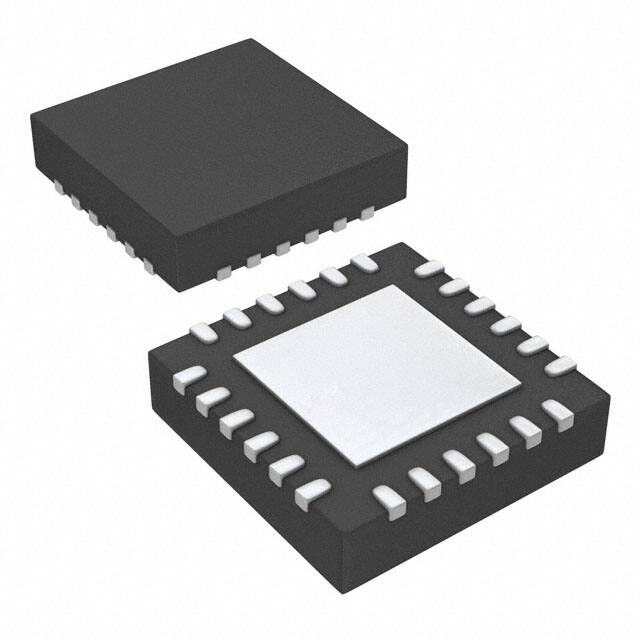
The DRV8300 family of devices is a gate driver for three-phase motor drive applications. These devices
decrease system component count, saves PCB space and cost by integrating three independent half-bridge
gate drivers and optional bootstrap diodes.
DRV8300 supports external N-channel high-side and low-side power MOSFETs and can drive 750-mA source,
1.5-A sink peak currents with total combined 30-mA average output current. The DRV8300 family of devices are
available in 0.5-mm pitch QFN and 0.65-mm pitch TSSOP surface-mount packages. The QFN size is 4 × 4 mm
(0.5-mm pin pitch) for the 24-pin package, and TSSOP size is 6.5 × 6.4 mm (0.65-mm pin pitch) for the 20-pin
package.
Submit Document Feedback
Copyright © 2021 Texas Instruments Incorporated
Product Folder Links: DRV8300
11
�DRV8300
www.ti.com
SLVSFG5C – SEPTEMBER 2020 – REVISED FEBRUARY 2021
8.2 Functional Block Diagram
GVDD
CGVDD
PVDD
GVDD
INHA
HS
INT_5V
BSTA
HS
GHA
CBSTA RGHA
SHA
GVDD
INLA/INLA
LS
LS
RGLA
GLA
MODE**
Gate Driver
GVDD
BSTB
PVDD
CBSTB
HS
INHB
INT_5V
Input logic
control
HS
MODE**
SHB
LS
LS
GLB
RGLB
Gate Driver
GVDD
INHC
RGHB
GVDD
INLB/INLB
ShootThrough
Prevention
GHB
HS
INT_5V
PVDD
BSTC
HS
GHC
CBSTC
RGHC
SHC
GVDD
INLC/INLC
LS
LS
GLC
RGLC
MODE**
DT**
Gate Driver
MODE**
GND
PowerPAD
** QFN-24 Package
Figure 8-1. Block Diagram for DRV8300D
12
Submit Document Feedback
Copyright © 2021 Texas Instruments Incorporated
Product Folder Links: DRV8300
�DRV8300
www.ti.com
SLVSFG5C – SEPTEMBER 2020 – REVISED FEBRUARY 2021
GVDD
CGVDD
GVDD
PVDD
BSTA
CBSTA
INHA
HS
INT_5V
HS
RGHA
GHA
SHA
GVDD
INLA/INLA
LS
LS
RGLA
GLA
MODE**
Gate Driver
BSTB
PVDD
CBSTB
HS
INHB
INT_5V
Input logic
control
HS
MODE**
RGHB
SHB
GVDD
INLB/INLB
ShootThrough
Prevention
GHB
LS
LS
GLB
RGLB
Gate Driver
PVDD
BSTC
INHC
HS
INT_5V
HS
GHC
CBSTC
RGHC
SHC
GVDD
INLC/INLC
LS
LS
GLC
RGLC
MODE**
Gate Driver
DT**
MODE**
GND
PowerPAD
** QFN-24 Package
Figure 8-2. Block Diagram for DRV8300N
Submit Document Feedback
Copyright © 2021 Texas Instruments Incorporated
Product Folder Links: DRV8300
13
�DRV8300
www.ti.com
SLVSFG5C – SEPTEMBER 2020 – REVISED FEBRUARY 2021
8.3 Feature Description
8.3.1 Three BLDC Gate Drivers
The DRV8300 integrates three half-bridge gate drivers, each capable of driving high-side and low-side Nchannel power MOSFETs. Input on GVDD provides the gate bias voltage for the low-side MOSFETs. The high
voltage is generated using bootstrap capacitor and GVDD supply. The half-bridge gate drivers can be used in
combination to drive a three-phase motor or separately to drive other types of loads.
8.3.1.1 Gate Drive Timings
8.3.1.1.1 Propagation Delay
The propagation delay time (tpd) is measured as the time between an input logic edge to a detected output
change. This time has two parts consisting of the input deglitcher delay and the delay through the analog gate
drivers.
The input deglitcher prevents high-frequency noise on the input pins from affecting the output state of the gate
drivers. The analog gate drivers have a small delay that contributes to the overall propagation delay of the
device.
8.3.1.1.2 Deadtime and Cross-Conduction Prevention
In the DRV8300, high- and low-side inputs operate independently, with an exception to prevent cross conduction
when high and low side are turned ON at same time. The DRV8300 turns OFF high- and low- side output to
prevent shoot through when high- and low-side inputs are logic high at same time.
The DRV8300 also provides deadtime insertion to prevents both external MOSFETs of each power-stage from
switching on at the same time. In devices with DT pin (QFN package device), deadtime can be linearily adjusted
between 200 nS to 2000 nS by connecting resistor between DT and ground. When DT pin left floating, fixed
deadtime of 200 nS (Typical value) is inserted. The value of resistor can be caculated using following equation.
4&6 (GÀ) =
&A=@PEIA (J5)
5
In device without DT pin (TSSOP package device), fixed deadtime of 200 nS (Typical value) is inserted to
prevent high and low side gate output turning on at same time.
INHx/INLx Inputs
INHx
INLx
GHx/GLx outputs
GHx
GLx
DT
DT
Cross
Conduction
Prevention
Figure 8-3. Cross Conduction Prevention and Deadtime Insertion
14
Submit Document Feedback
Copyright © 2021 Texas Instruments Incorporated
Product Folder Links: DRV8300
�DRV8300
www.ti.com
SLVSFG5C – SEPTEMBER 2020 – REVISED FEBRUARY 2021
8.3.1.2 Mode (Inverting and non inverting INLx)
The DRV8300 has flexibility of accepting different kind of inputs on INLx. In devices with MODE pin (QFN
package device), the DRV8300 provides option of GLx output inverted or non-inverted compared to polarity of
signal on INLx pin. When MODE pin is left floating INLx is configured to be in non-inverting mode and GLx
output is in phase with INLx (see Figure 8-4), whereas when MODE pin is connected to GVDD, GLx output is out
of phase with inputs (see Figure 8-5). In devices without MODE pin (TSSOP package device), there are different
device option available for inverting and non inverting inputs (see Section 5)
INHx
INLx
GHx
GLx
DT
DT
DT
Figure 8-4. Non-Inverted INLx inputs
INHx
INLx
GHx
GLx
DT
DT
DT
Figure 8-5. Inverted INLx inputs
Submit Document Feedback
Copyright © 2021 Texas Instruments Incorporated
Product Folder Links: DRV8300
15
�DRV8300
www.ti.com
SLVSFG5C – SEPTEMBER 2020 – REVISED FEBRUARY 2021
8.3.2 Pin Diagrams
Figure 8-6 shows the input structure for the logic level pins INHx, INLx. INHx and INLx has passive pull down, so
when inputs are floating the output of gate driver will be pulled low. Figure 8-7 shows the input structure for the
logic level pin inverted INLx. INLx in inverted mode has passive pull up, so when inputs are floating the output of
gate driver will be pulled low.
INT_5V
INPUT
INPUT
200 k
Logic High
Logic High
INHx
INLx
INLx
Logic Low
Logic Low
200 k
Figure 8-6. INHx and non-inverted INLx Logic-Level
Input Pin Structure
Figure 8-7. Inverted INLx Logic-Level Input Pin
Structure
8.3.3 Gate Driver Protective Circuits
The DRV8300 is protected against BSTx undervoltage and GVDD undervoltage events.
Table 8-1. Fault Action and Response
FAULT
CONDITION
GATE DRIVER
RECOVERY
VBSTx undervoltage
(BSTUV)
VBSTx < VBSTUV
GHx - Hi-Z
Automatic:
VBSTx > VBSTUV and low to high
PWM edge detected on INHx pin
GVDD undervoltage
(GVDDUV)
VGVDD < VGVDDUV
Hi-Z
Automatic:
VGVDD > VGVDDUV
8.3.3.1 VBSTx Undervoltage Lockout (BSTUV)
The DRV8300 has separate voltage comparator to detect undervoltage condition for each phase. If at any time
the supply voltage on the BSTx pin falls lower than the VBSTUV threshold, high side external MOSFETs of that
particular phase is disabled by disabling (Hi-Z) GHx pin. Normal operation starts again when the BSTUV
condition clears and low to high PWM edge is detected on INHx input on the same phase BSTUV was detected.
BSTUV protection ensures that high side gate driver are not switched when BSTx pin has lower value.
8.3.3.2 GVDD Undervoltage Lockout (GVDDUV)
If at any time the voltage on the GVDD pin falls lower than the VGVDDUV threshold voltage, all of the external
MOSFETs are disabled. Normal operation starts again GVDDUV condition clears. GVDDUV protection ensures
that gate driver are not switched when GVDD input is at lower value.
8.4 Device Functional Modes
Whenever the GVDD > VGVDDUVand VBSTX > VBSTUV the device is in operating (active) mode, in this condition
gate driver output GHx and GLX will follow respective inputs INHx and INLx.
16
Submit Document Feedback
Copyright © 2021 Texas Instruments Incorporated
Product Folder Links: DRV8300
�DRV8300
www.ti.com
SLVSFG5C – SEPTEMBER 2020 – REVISED FEBRUARY 2021
9 Application and Implementation
Note
Information in the following applications sections is not part of the TI component specification, and TI
does not warrant its accuracy or completeness. TI’s customers are responsible for determining
suitability of components for their purposes. Customers should validate and test their design
implementation to confirm system functionality.
9.1 Application Information
The DRV8300 family of devices is primarily used in applications for three-phase brushless DC motor control. The
design procedures in the Section 9.2 section highlight how to use and configure the DRV8300.
Submit Document Feedback
Copyright © 2021 Texas Instruments Incorporated
Product Folder Links: DRV8300
17
�DRV8300
www.ti.com
SLVSFG5C – SEPTEMBER 2020 – REVISED FEBRUARY 2021
9.2 Typical Application
GVDD
GVDD
CGVDD
PVDD
GND
External
Supply
GND
BSTA
CBSTA RGHA
GHA
SHA
RGLA
INHA
GLA
INLA
INHB
PWM
MCU
INLB
PVDD
BSTB
INHC
INLC
CBSTB
RGHB
GHB
ADC
SHB
RGLB
DRV8300D
GLB
GVDD
MODE**
PVDD
BSTC
BSTC
CBSTC
RGHC
GHC
GND or Floating
GHC
SHC
SHC
RDT
DT**
RGLC
GLC
** QFN-24 Package
GLC
RSENSE
INC+
RSENSE
R
INB+
RSENSE
INA+
INA-
INB-
INC-
R
R
R
OUT
±
OUT
OUT
Reference
Voltage
± +
VREF
VREF
IN- INx+
IN-IN+
RR
IN-IN+
R
IN+
INx-
R
R
VREF
R
± +
R
+
R R
R
+
Current Sense Amplifier 1x or 3x
±
Figure 9-1. Application Schematic
18
Submit Document Feedback
Copyright © 2021 Texas Instruments Incorporated
Product Folder Links: DRV8300
�DRV8300
www.ti.com
SLVSFG5C – SEPTEMBER 2020 – REVISED FEBRUARY 2021
9.2.1 Design Requirements
Table 9-1 lists the example design input parameters for system design.
Table 9-1. Design Parameters
EXAMPLE DESIGN PARAMETER
REFERENCE
EXAMPLE VALUE
-
CSD19532Q5B
MOSFET
Gate Supply Voltage
Gate Charge
VGVDD
12 V
QG
48 nC
9.2.2 Detailed Design Procedure
Bootstrap Capacitor and GVDD Capacitor Selection
The bootstrap capacitor must be sized to maintain the bootstrap voltage above the undervoltage lockout for
normal operation. Equation 1 calculates the maximum allowable voltage drop across the bootstrap capacitor:
¿8$56: = 8)8&& F 8$116& F 8$5678
(1)
=12 V – 0.85 V – 4.5 V = 6.65 V
where
• VGVDD is the supply voltage of the gate drive
• VBOOTD is the forward voltage drop of the bootstrap diode
• VBSTUV is the threshold of the bootstrap undervoltage lockout
In this example the allowed voltage drop across bootstrap capacitor is 6.65 V. It is generally recommended that
ripple voltage on both the bootstrap capacitor and GVDD capacitor should be minimized as much as possible.
Many of commercial, industrial, and automotive applications use ripple value between 0.5 V to 1 V.
The total charge needed per switching cycle can be estimated with Equation 2:
3616 = 3) +
+.$5_64#05
B59
(2)
=48 nC + 220 μA/20 kHz = 50 nC + 11 nC = 59 nC
where
• QG is the total MOSFET gate charge
• ILBS_TRAN is the bootstrap pin leakage current
• fSW is the is the PWM frequency
The minimum bootstrap capacitor an then be estimated as below assuming 1V ΔVBSTx:
%$56_/+0 = 3616W¿8
(3)
$56:
= 59 nC / 1 V = 59 nF
The calculated value of minimum bootstrap capacitor is 59 nF. It should be noted that, this value of capacitance
is needed at full bias voltage. In practice, the value of the bootstrap capacitor must be greater than calculated
value to allow for situations where the power stage may skip pulse due to various transient conditions. It is
recommended to use a 100 nF bootstrap capacitor in this example. It is also recommenced to include enough
margin and place the bootstrap capacitor as close to the BSTx and SHx pins as possible.
Submit Document Feedback
Copyright © 2021 Texas Instruments Incorporated
Product Folder Links: DRV8300
19
�DRV8300
www.ti.com
SLVSFG5C – SEPTEMBER 2020 – REVISED FEBRUARY 2021
Note
If device variants (DRV8300D) with integrated bootstrap diode are used with bootstrap capacitor value
(CBSTx) above 1 μF, than current flowing through internal bootstrap diode needs to be limited.
The local GVDD bypass capacitor must be greater than the value of bootstrap capacitor value (generally 10
times the bootstrap capacitor value).
%)8&& R 10 × %$56:
(4)
= 10*100 nF= 1 μF
For this example application choose 1 µF CGVDD capacitor. Choose a capacitor with a voltage rating at least
twice the maximum voltage that it will be exposed to because most ceramic capacitors lose significant
capacitance when biased. This value also improves the long term reliability of the system.
Gate Resistance Selection
The slew rate of the SHx connection will be dependent on the rate at which the gate of the external MOSFETs is
controlled. The pull-up/pull-down strength of the DRV8300 is fixed internally, hence slew rate of gate voltage can
be controlled with an external series gate resistor. In some applications the gate charge, which is load on gate
driver device, is significantly larger than gate driver peak output current capability. In such applications external
gate resistors can limit the peak output current of the gate driver. External gate resistors are also used to damp
ringing and noise.
The specific parameters of the MOSFET, system voltage, and board parasitics will all affect the final slew rate,
so generally selecting an optimal value or configuration of external gate resistor is an iterative process.
9.2.3 Application Curves
GHA
GHA
SHA
SHA
GLA
GLA
Figure 9-2. Gate voltages, SHx rising with 15 ohm
gate resistor and CSD19532Q5B MOSFET
20
Figure 9-3. Gate voltages, SHx falling with 15 ohm
gate resistor and CSD19532Q5B MOSFET
Submit Document Feedback
Copyright © 2021 Texas Instruments Incorporated
Product Folder Links: DRV8300
�DRV8300
www.ti.com
SLVSFG5C – SEPTEMBER 2020 – REVISED FEBRUARY 2021
10 Power Supply Recommendations
The DRV8300 is designed to operate from an input voltage supply (GVDD) range from 4.8 V to 20 V. A local
bypass capacitor should be placed between the GVDD and GND pins. This capacitor should be located as close
to the device as possible. A low ESR, ceramic surface mount capacitor is recommended. It is recommended to
use two capacitors across GVDD and GND: a low capacitance ceramic surface-mount capacitor for high
frequency filtering placed very close to GVDD and GND pin, and another high capacitance value surfacemount
capacitor for device bias requirements. In a similar manner, the current pulses delivered by the GHx pins are
sourced from the BSTx pins. Therefore, capacitor across the BSTx to SHx is recommended, it should be high
enough capacitance value capacitor to deliver GHx pulses
Submit Document Feedback
Copyright © 2021 Texas Instruments Incorporated
Product Folder Links: DRV8300
21
�DRV8300
www.ti.com
SLVSFG5C – SEPTEMBER 2020 – REVISED FEBRUARY 2021
11 Layout
11.1 Layout Guidelines
•
•
•
•
•
•
•
•
Low ESR/ESL capacitors must be connected close to the device between GVDD and GND and between
BSTx and SHx pins to support high peak currents drawn from GVDD and BSTx pins during the turn-on of the
external MOSFETs.
To prevent large voltage transients at the drain of the top MOSFET, a low ESR electrolytic capacitor and a
good quality ceramic capacitor must be connected between the high side MOSFET drain and ground.
In order to avoid large negative transients on the switch node (SHx) pin, the parasitic inductances between
the source of the high-side MOSFET and the source of the low-side MOSFET must be minimized.
In order to avoid unexpected transients, the parasitic inductance of the GHx, SHx, and GLx connections must
be minimized. Minimize the trace length and number of vias wherever possible. Minimum 10 mil and typical
15 mil trace width is recommended.
Resistance between DT and GND must be place as close as possible to device
Place the gate driver as close to the MOSFETs as possible. Confine the high peak currents that charge and
discharge the MOSFET gates to a minimal physical area by reducing trace length. This confinement
decreases the loop inductance and minimize noise issues on the gate terminals of the MOSFETs.
In QFN package device variants, NC pins can be connected to GND to increase ground conenction between
thermal pad and external ground plane.
Refer to sections General Routing Techniques and MOSFET Placement and Power Stage Routing in
Application Report
11.2 Layout Example
DT resistor
close to device
BSTx capacitor close
to device
GVDD capacitor
close to device
22
Submit Document Feedback
Copyright © 2021 Texas Instruments Incorporated
Product Folder Links: DRV8300
�DRV8300
www.ti.com
SLVSFG5C – SEPTEMBER 2020 – REVISED FEBRUARY 2021
12 Device and Documentation Support
12.1 Receiving Notification of Documentation Updates
To receive notification of documentation updates, navigate to the device product folder on ti.com. Click on
Subscribe to updates to register and receive a weekly digest of any product information that has changed. For
change details, review the revision history included in any revised document.
12.2 Support Resources
TI E2E™ support forums are an engineer's go-to source for fast, verified answers and design help — straight
from the experts. Search existing answers or ask your own question to get the quick design help you need.
Linked content is provided "AS IS" by the respective contributors. They do not constitute TI specifications and do
not necessarily reflect TI's views; see TI's Terms of Use.
12.3 Trademarks
TI E2E™ is a trademark of Texas Instruments.
All trademarks are the property of their respective owners.
12.4 Electrostatic Discharge Caution
This integrated circuit can be damaged by ESD. Texas Instruments recommends that all integrated circuits be handled
with appropriate precautions. Failure to observe proper handling and installation procedures can cause damage.
ESD damage can range from subtle performance degradation to complete device failure. Precision integrated circuits may
be more susceptible to damage because very small parametric changes could cause the device not to meet its published
specifications.
12.5 Glossary
TI Glossary
This glossary lists and explains terms, acronyms, and definitions.
13 Mechanical, Packaging, and Orderable Information
The following pages include mechanical, packaging, and orderable information. This information is the most
current data available for the designated devices. This data is subject to change without notice and revision of
this document. For browser-based versions of this data sheet, refer to the left-hand navigation.
Submit Document Feedback
Copyright © 2021 Texas Instruments Incorporated
Product Folder Links: DRV8300
23
�PACKAGE OPTION ADDENDUM
www.ti.com
23-Aug-2021
PACKAGING INFORMATION
Orderable Device
Status
(1)
Package Type Package Pins Package
Drawing
Qty
Eco Plan
(2)
Lead finish/
Ball material
MSL Peak Temp
Op Temp (°C)
Device Marking
(3)
(4/5)
(6)
DRV8300DIPWR
ACTIVE
TSSOP
PW
20
3000
RoHS & Green
NIPDAU
Level-2-260C-1 YEAR
-40 to 125
8300DI
DRV8300DPWR
ACTIVE
TSSOP
PW
20
3000
RoHS & Green
NIPDAU
Level-2-260C-1 YEAR
-40 to 125
8300D
DRV8300DRGER
ACTIVE
VQFN
RGE
24
3000
RoHS & Green
NIPDAU
Level-1-260C-UNLIM
-40 to 125
8300D
DRV8300NIPWR
ACTIVE
TSSOP
PW
20
3000
RoHS & Green
NIPDAU
Level-2-260C-1 YEAR
-40 to 125
8300NI
DRV8300NPWR
ACTIVE
TSSOP
PW
20
3000
RoHS & Green
NIPDAU
Level-2-260C-1 YEAR
-40 to 125
8300N
DRV8300NRGER
ACTIVE
VQFN
RGE
24
3000
RoHS & Green
NIPDAU
Level-1-260C-UNLIM
-40 to 125
8300N
(1)
The marketing status values are defined as follows:
ACTIVE: Product device recommended for new designs.
LIFEBUY: TI has announced that the device will be discontinued, and a lifetime-buy period is in effect.
NRND: Not recommended for new designs. Device is in production to support existing customers, but TI does not recommend using this part in a new design.
PREVIEW: Device has been announced but is not in production. Samples may or may not be available.
OBSOLETE: TI has discontinued the production of the device.
(2)
RoHS: TI defines "RoHS" to mean semiconductor products that are compliant with the current EU RoHS requirements for all 10 RoHS substances, including the requirement that RoHS substance
do not exceed 0.1% by weight in homogeneous materials. Where designed to be soldered at high temperatures, "RoHS" products are suitable for use in specified lead-free processes. TI may
reference these types of products as "Pb-Free".
RoHS Exempt: TI defines "RoHS Exempt" to mean products that contain lead but are compliant with EU RoHS pursuant to a specific EU RoHS exemption.
Green: TI defines "Green" to mean the content of Chlorine (Cl) and Bromine (Br) based flame retardants meet JS709B low halogen requirements of


 工商网监
湘ICP备2023018690号
工商网监
湘ICP备2023018690号
