Sample &
Buy
Product
Folder
Support &
Community
Tools &
Software
Technical
Documents
Reference
Design
DRV8313
SLVSBA5D – OCTOBER 2012 – REVISED APRIL 2016
DRV8313 2.5-A Triple 1/2-H Bridge Driver
1 Features
3 Description
•
The DRV8313 provides three individually controllable
half-H-bridge drivers. The device is intended to drive
a three-phase brushless-DC motor, although it can
also be used to drive solenoids or other loads. Each
output driver channel consists of N-channel power
MOSFETs configured in a 1/2-H-bridge configuration.
Each 1/2-H-bridge driver has a dedicated ground
terminal, which allows independent external current
sensing.
1
•
•
•
•
•
•
•
•
Triple 1/2-H Bridge Driver IC
– 3-Phase brushless DC Motors
– Solenoid and Brushed DC Motors
High Current-Drive Capability: 2.5-A Peak
Low MOSFET ON-Resistance
Independent 1/2-H-Bridge Control
Uncommitted Comparator Can Be Used for
Current Limit or Other Functions
Built-In 3.3-V 10-mA LDO Regulator
8-V to 60-V Operating Supply-Voltage Range
Sleep Mode for Standby Operation
Small Package and Footprint
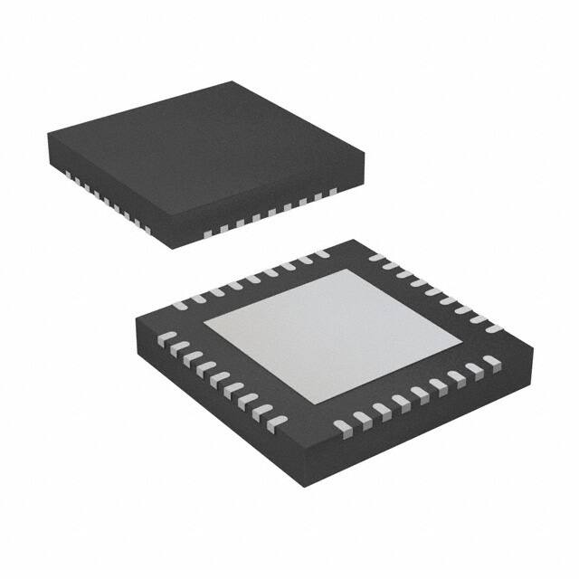
– 28-Pin HTSSOP (PowerPAD™ Package)
– 36-Pin VQFN
An uncommitted comparator is integrated into the
DRV8313, which allows for the construction of
current-limit circuitry or other functions.
Internal protection functions are provided for
undervoltage, charge pump faults, overcurrent, short
circuits, and overtemperature. Fault conditions are
indicated by the nFAULT pin.
Device Information(1)
2 Applications
•
•
•
•
PART NUMBER
Camera Gimbals
HVAC Motors
Office Automation Machines
Factory Automation and Robotics
DRV8313
PACKAGE
BODY SIZE (NOM)
HTSSOP (28)
9.70 mm × 4.40 mm
VQFN (36)
6.00 mm × 6.00 mm
(1) For all available packages, see the orderable addendum at
the end of the data sheet.
Simplified Schematic
8 to 60 V
DRV8313
3.5 A
Controller
IN
EN
nSLEEP
3 ½-H Bridge
Driver
M
nFAULT
Built-In Protection
3.3 V
10 mA
3.3-V LDO
Copyright © 2016, Texas Instruments Incorporated
1
An IMPORTANT NOTICE at the end of this data sheet addresses availability, warranty, changes, use in safety-critical applications,
intellectual property matters and other important disclaimers. PRODUCTION DATA.
�DRV8313
SLVSBA5D – OCTOBER 2012 – REVISED APRIL 2016
www.ti.com
Table of Contents
1
2
3
4
5
6
7
Features ..................................................................
Applications ...........................................................
Description .............................................................
Revision History.....................................................
Pin Configuration and Functions .........................
Specifications.........................................................
1
1
1
2
3
4
6.1
6.2
6.3
6.4
6.5
6.6
6.7
4
4
5
5
6
7
8
Absolute Maximum Ratings ......................................
ESD Ratings ............................................................
Recommended Operating Conditions.......................
Thermal Information .................................................
Electrical Characteristics...........................................
Switching Characteristics ..........................................
Typical Characteristics ..............................................
Detailed Description ............................................ 10
7.1
7.2
7.3
7.4
Overview .................................................................
Functional Block Diagram .......................................
Feature Description.................................................
Device Functional Modes........................................
10
10
11
14
8
Application and Implementation ........................ 15
8.1 Application Information............................................ 15
8.2 Typical Applications ................................................ 15
9
Power Supply Recommendations...................... 22
9.1 Bulk Capacitance .................................................... 22
10 Layout................................................................... 23
10.1
10.2
10.3
10.4
Layout Guidelines .................................................
Layout Example ....................................................
Thermal Considerations ........................................
Power Dissipation .................................................
23
23
25
25
11 Device and Documentation Support ................. 26
11.1
11.2
11.3
11.4
11.5
Documentation Support ........................................
Community Resources..........................................
Trademarks ...........................................................
Electrostatic Discharge Caution ............................
Glossary ................................................................
26
26
26
26
26
12 Mechanical, Packaging, and Orderable
Information ........................................................... 26
4 Revision History
NOTE: Page numbers for previous revisions may differ from page numbers in the current version.
Changes from Revision C (November 2015) to Revision D
•
Page
Changed pin 18 of the VQFN (RHH) package from GND to RSVD ...................................................................................... 4
Changes from Revision B (January 2015) to Revision C
Page
•
Added a new package to the Device Information table ......................................................................................................... 1
•
Added a new VQFN package for the device ......................................................................................................................... 3
•
Corrected a numbering error on one of the ground pins in the Pin Functions table ............................................................. 3
Changes from Revision A (November 2012) to Revision B
•
2
Page
Added ESD Ratings table, Feature Description section, Device Functional Modes, Application and Implementation
section, Power Supply Recommendations section, Layout section, Device and Documentation Support section, and
Mechanical, Packaging, and Orderable Information section ................................................................................................. 4
Submit Documentation Feedback
Copyright © 2012–2016, Texas Instruments Incorporated
Product Folder Links: DRV8313
�DRV8313
www.ti.com
SLVSBA5D – OCTOBER 2012 – REVISED APRIL 2016
5 Pin Configuration and Functions
PWP Package
28-Pin HTSSOP With PowerPAD Package
Top View
7
22
EN3
OUT2
8
21
NC
GND
nCOMPO
nFAULT
28
3
25
V3P3
24
GND
23
GND
NC
4
CPL
5
CPH
6
22
COMPN
VCP
7
21
COMPP
NC
8
20
GND
VM
9
19
VM
Thermal
Pad
COMPN
13
16
nRESET
GND
14
15
V3P3
NC - No internal connection
18
nSLEEP
RSVD
17
17
12
GND
COMPP
16
nFAULT
15
18
OUT3
11
PGND3
VM
14
nCOMPO
13
19
NC
10
OUT2
PGND3
12
GND
PGND2
20
nRESET
GND
11
9
nSLEEP
26
IN3
PGND2
OUT3
27
2
10
23
1
IN1
OUT1
6
EN1
PGND1
PGND1
29
EN2
GND
IN2
24
30
25
5
31
4
GND
VM
OUT1
EN3
EN1
32
26
33
3
IN3
IN1
VCP
EN2
GND
27
34
28
2
IN2
1
35
CPL
CPH
36
RHH Package
36-Pin VQFN With Exposed Thermal Pad
Top View
Pin Functions
PIN
NAME
TYPE (1)
NO.
DESCRIPTION
PWP
RHH
COMPN
13
22
I
Comparator negative input. Uncommitted comparator input
COMPP
12
21
I
Comparator positive input. Uncommitted comparator input
CPL
1
5
PWR
Charge pump. Connect a VM-rated, 0.01-µF ceramic capacitor between CPH and
CPL.
CPH
2
6
PWR
Charge pump. Connect a VM-rated, 0.01-µF ceramic capacitor between CPH and
CPL.
EN1
26
1
I
Channel enable. Logic high enables the 1/2-H bridge channel; internal pulldown
EN2
24
35
I
Channel enable. Logic high enables the 1/2-H bridge channel; internal pulldown
EN3
22
33
I
Channel enable. Logic high enables the 1/2-H bridge channel; internal pulldown
14, 20, 28
3, 17, 20,
23, 24, 30,
31, 32,
PWR
IN1
27
2
I
Channel input. Logic high pulls 1/2-H bridge high, logic low pulls 1/2-H bridge low; no
effect when ENx is low; internal pulldown input.
IN2
25
36
I
Channel input. Logic high pulls 1/2-H bridge high, logic low pulls 1/2-H bridge low; no
effect when ENx is low; internal pulldown input.
IN3
23
34
I
Channel input. Logic high pulls 1/2-H bridge high, logic low pulls 1/2-H bridge low; no
effect when ENx is low; internal pulldown input.
NC
21
4, 8, 14
NC
No internal connection. Recommended net given in block diagram (if any)
nCOMPO
19
29
OD
Comparator output. Uncommitted comparator output; open drain requires an external
pullup.
nFAULT
18
28
OD
Fault indication pin. Pulled logic-low with fault condition; open-drain output requires an
external pullup.
nRESET
16
26
I
GND
(1)
Device ground. Connect to system ground
Reset input. Active-low reset input initializes internal logic, clears faults, and disables
the outputs, internal pulldown
I = input, O = output, OD = open-drain output, PWR = power, NC = no connect
Submit Documentation Feedback
Copyright © 2012–2016, Texas Instruments Incorporated
Product Folder Links: DRV8313
3
�DRV8313
SLVSBA5D – OCTOBER 2012 – REVISED APRIL 2016
www.ti.com
Pin Functions (continued)
PIN
TYPE (1)
NO.
NAME
DESCRIPTION
PWP
RHH
nSLEEP
17
27
I
Sleep mode input. Logic high to enable device; logic low to enter low-power sleep
mode; internal pulldown
OUT1
5
10
O
Half-H bridge output, connect to the load
OUT2
8
13
O
Half-H bridge output, connect to the load
OUT3
9
15
O
Half-H bridge output, connect to the load
PGND1
6
11
PWR
Low-side FET source. Connect to GND or to low-side current-sense resistors
PGND2
7
12
PWR
Low-side FET source. Connect to GND or to low-side current-sense resistors
PGND3
10
16
PWR
Low-side FET source. Connect to GND or to low-side current-sense resistors
RSVD
—
18
—
V3P3
15
25
PWR
Internal regulator. Internal supply voltage; bypass to GND with a 6.3-V, 0.47-µF
ceramic capacitor; up to 10-mA external load
VCP
3
7
PWR
Charge pump. Connect a 16-V, 0.1-µF ceramic capacitor to VM
VM
4, 11
9, 19
PWR
Power supply. Connect to motor supply voltage; bypass to GND with two 0.1-µF
capacitors (for each pin) plus one bulk capacitor rated for VM
PWR
Must be connected to ground
Thermal pad
Reserved. Leave this pin disconnected.
6 Specifications
6.1 Absolute Maximum Ratings
over operating free-air temperature range (unless otherwise noted) (1) (2)
MIN
MAX
–0.3
65
V
0
2
V/µs
Charge pump voltage (VCP, CPH)
–0.3
VM + 12
V
Charge pump negative switching pin (CPL)
–0.3
VM
V
0
10
mA
Internal regulator voltage (V3P3)
–0.3
3.8
V
Control pin voltage (nRESET, nSLEEP, nFAULT, nCOMPO, ENx, INx)
–0.5
7
V
Comparator input-voltage (COMPP, COMPN)
–0.5
7
V
0
10
mA
Continuous phase node pin voltage (OUTx)
–0.7
VM + 0.7
V
Continuous 1/2-H-bridge source voltage (PGNDx)
–600
600
mV
Power-supply voltage (VM)
Power supply voltage ramp rate (VM)
Internal regulator current output (V3P3)
Open drain output current (nFAULT, nCOMPO)
Peak output current (OUTx)
Internally limited
UNIT
A
Operating junction temperature TJ
–40
150
°C
Storage temperature Tstg
–60
150
°C
(1)
(2)
Stresses beyond those listed under Absolute Maximum Ratings may cause permanent damage to the device. These are stress ratings
only, and do not imply functional operation of the device at these or any other conditions beyond those indicated under Recommended
Operating Conditions. Exposure to absolute-maximum-rated conditions for extended periods may affect device reliability.
All voltage values are with respect to the network ground terminal.
6.2 ESD Ratings
VALUE
V(ESD)
(1)
(2)
4
Electrostatic discharge
Human body model (HBM), per ANSI/ESDA/JEDEC JS-001 (1)
±3000
Charged device model (CDM), per JEDEC specification JESD22-C101 (2)
±1500
UNIT
V
JEDEC document JEP155 states that 500-V HBM allows safe manufacturing with a standard ESD control process.
JEDEC document JEP157 states that 250-V CDM allows safe manufacturing with a standard ESD control process.
Submit Documentation Feedback
Copyright © 2012–2016, Texas Instruments Incorporated
Product Folder Links: DRV8313
�DRV8313
www.ti.com
SLVSBA5D – OCTOBER 2012 – REVISED APRIL 2016
6.3 Recommended Operating Conditions
over operating free-air temperature range (unless otherwise noted)
MIN
(1)
MAX
UNIT
VM
Motor power-supply voltage
8
60
VIN
Digital pin voltage
0
5.5
V
fPWM
Applied PWM signal on ENx, INx
0
250
kHz
VGNDX
PGNDx pin voltage
–500
500
mV
0
(2)
mA
125
°C
IV3P3
V3P3 load current
TA
Operating ambient temperature
(1)
(2)
10
–40
V
Both VM pins must be connected to the same supply voltage.
Power dissipation and thermal limits must be observed.
6.4 Thermal Information
DRV8313
THERMAL METRIC
(1)
PWP (HTSSOP)
RHH (VQFN)
28 PINS
36 PINS
UNIT
RθJA
Junction-to-ambient thermal resistance
31.6
31.1
°C/W
RθJC(top)
Junction-to-case (top) thermal resistance
15.9
17.3
°C/W
RθJB
Junction-to-board thermal resistance
5.6
5.6
°C/W
ψJT
Junction-to-top characterization parameter
0.2
0.2
°C/W
ψJB
Junction-to-board characterization parameter
5.5
5.6
°C/W
RθJC(bot)
Junction-to-case (bottom) thermal resistance
1.4
1.3
°C/W
(1)
For more information about traditional and new thermal metrics, see the Semiconductor and IC Package Thermal Metrics application
report, SPRA953.
Submit Documentation Feedback
Copyright © 2012–2016, Texas Instruments Incorporated
Product Folder Links: DRV8313
5
�DRV8313
SLVSBA5D – OCTOBER 2012 – REVISED APRIL 2016
www.ti.com
6.5 Electrical Characteristics
TA = 25°C, over operating free-air temperature range (unless otherwise noted)
PARAMETER
TEST CONDITIONS
MIN
TYP
MAX
UNIT
POWER SUPPLIES
IVM
VM operating supply current
VM = 24 V, fPWM < 50 kHz
IVMQ
VM sleep-mode supply current
VM = 24 V
1
5
mA
500
800
µA
3.3
3.52
V
0.6
0.7
V
INTERNAL REGULATOR (V3P3)
V3P3
V3P3 voltage
IOUT = 0 to 10 mA
3.1
LOGIC-LEVEL INPUTS (nSLEEP, ENx, INx)
VIL
Input low voltage
VIH
Input high voltage
2.2
5.25
V
VHYS
Input hysteresis
50
600
mV
IIL
Input low current
VIN = 0
–5
5
µA
IIH
Input high current
VIN = 3.3 V
RPD
Pulldown resistance
100
100
µA
kΩ
OPEN-DRAIN OUTPUTS (nFAULT and nCOMPO)
VOL
Output low voltage
IO = 5 mA
IOH
Output high leakage current
VO = 3.3 V
0.5
V
1
µA
5
V
–7
7
mV
–300
300
nA
2
µs
COMPARATOR (COMPP, COMPN, nCOMPO)
VCM
Common-mode input-voltage range
VIO
Input offset voltage
IIB
Input bias current
tR
Response time
0
100-mV step with 10-mV overdrive
H-BRIDGE FETs
High-side FET ON-resistance
rDS(on)
Low-side FET ON-resistance
IOFF
VM = 24 V, IO = 1 A, TJ = 25°C
0.24
VM = 24 V, IO = 1 A, TJ = 85°C (1)
0.29
VM = 24 V, IO = 1 A, TJ = 25°C
0.24
VM = 24 V, IO = 1 A, TJ = 85°C
(1)
Off-state leakage current
0.29
–2
0.39
0.39
Ω
Ω
2
µA
8
V
PROTECTION CIRCUITS
VUVLO
VM undervoltage lockout voltage
IOCP
Overcurrent protection trip level
tOCP
Overcurrent protection deglitch time
TTSD (1)
Thermal shutdown temperature
Die temperature
THYS (1)
Thermal shutdown hysteresis
Die temperature
(1)
6
VM rising
6.3
3
150
5
A
5
µs
160
35
180
°C
°C
Specification based on design and characterization data
Submit Documentation Feedback
Copyright © 2012–2016, Texas Instruments Incorporated
Product Folder Links: DRV8313
�DRV8313
www.ti.com
SLVSBA5D – OCTOBER 2012 – REVISED APRIL 2016
6.6 Switching Characteristics
TA = 25°C, VM = 24 V, RL = 20 Ω
PARAMETER
TEST CONDITIONS
MIN
TYP MAX UNIT
t1
Delay time, ENx high to OUTx high
INx = 1
130
330
ns
t2
Delay time, ENx low to OUTx low
INx = 1
275
475
ns
t3
Delay time, ENx high to OUTx low
INx = 0
100
300
ns
t4
Delay time, ENx low to OUTx high
INx = 0
200
400
ns
t5
Delay time, INx high to OUTx high
ENx = 1
300
500
ns
t6
Delay time, INx low to OUTx low
ENx = 1
275
475
ns
tr
Output rise time, resistive load to GND
30
150
ns
tf
Output fall time, resistive load to GND
30
150
ns
tDEAD
Output dead time
(1)
(1)
90
ns
Specified by design and characterization data
ENx
50%
50%
ENx
t1
OUTx
50%
t2
50%
50%
t3
OUTx
50%
50%
t4
50%
INx = 0, Resistive Load to VM
INx = 1, Resistive Load to GND
INx
50%
50%
t5
t6
80%
80%
OUTx
OUTx
50%
50%
20%
20%
tr
tf
ENx = 1, Resistive Load to GND
T0543-01
Figure 1. DRV8313 Switching Characteristics
Submit Documentation Feedback
Copyright © 2012–2016, Texas Instruments Incorporated
Product Folder Links: DRV8313
7
�DRV8313
SLVSBA5D – OCTOBER 2012 – REVISED APRIL 2016
www.ti.com
6.7 Typical Characteristics
1.35
1.3
1.3
1.25
1.25
Supply Current IVM (mA)
1.2
1.15
1.1
1.05
1
0.95
TA = +125°C
TA = +85°C
TA = +25°C
TA = -40°C
0.9
0.85
10
15
20
25
30 35
VM (V)
40
45
50
55
0.8
-40
60
0
20
40
60
80
100
Ambient Temperature (qC)
120
140
D002
Figure 3. Supply Current vs Temperature at VM = 24 V
640
620
600
Sleep Current IVMQ (PA)
Sleep Current IVMQ (PA)
-20
D001
660
640
620
600
580
560
540
520
500
480
460
440
420
400
TA = +125°C
TA = +85°C
TA = +25°C
TA = -40°C
5
10
15
20
25
30 35
VM (V)
40
45
50
55
580
560
540
520
500
480
460
440
420
-40
60
-20
0
D003
20
40
60
80
100
Ambient Temperature (qC)
120
140
D004
Figure 5. Sleep Current vs Temperature at VM = 24 V
Figure 4. Sleep Current vs Supply Voltage
70
60
TA = +125°C
TA = +85°C
TA = +25°C
TA = -40°C
50
Relative to 24 V, 25qC
50
40
30
20
10
0
-10
High-Side RDS(ON) Change (%)
60
High-Side RDS(ON) Change (%)
1
0.95
0.9
Figure 2. Supply Current vs Supply Voltage
40
30
20
10
0
-10
-20
-20
-30
5
10
15
20
25
30
35
Supply Voltage VM (V)
40
45
50
-30
-40
-20
D005
Figure 6. High-Side RDS(on) vs Supply Voltage (Normalized to
24 V, 25°C)
8
1.1
1.05
0.85
0.8
5
1.2
1.15
Relative to 24 V, 25qC
Supply Current IVM (mA)
1.35
0
20
40
60
80
100
Ambient Temperature T A (qC)
120
140
D006
Figure 7. High-Side RDS(on) vs Temperature at VM = 24 V
(Normalized to 25°C)
Submit Documentation Feedback
Copyright © 2012–2016, Texas Instruments Incorporated
Product Folder Links: DRV8313
�DRV8313
www.ti.com
SLVSBA5D – OCTOBER 2012 – REVISED APRIL 2016
Typical Characteristics (continued)
70
60
TA = +125°C
TA = +85°C
TA = +25°C
TA = -40°C
50
30
20
10
0
-10
40
Relative to 24 V, 25qC
40
Low-Side RDS(ON) Change (%)
50
Relative to 24 V, 25qC
Low-Side RDS(ON) Change (%)
60
30
20
10
0
-10
-20
-20
-30
5
10
15
20
25
30
35
Supply Voltage VM (V)
40
45
-30
-40
50
-20
0
20
40
60
80
100
Ambient Temperature T A (qC)
D007
Figure 8. Low-Side RDS(on) vs Supply Voltage (Normalized to
24 V, 25°C)
120
140
D008
Figure 9. Low-Side RDS(on) vs Temperature at VM = 24 V
(Normalized to 25°C)
3.3
TA = +125°C
TA = +85°C
TA = +25°C
TA = -40°C
3.29
3.28
V3P3 (V)
3.27
3.26
3.25
3.24
3.23
3.22
3.21
0
1
2
3
4
5
6
Output Load (mA)
7
8
9
10
D009
Figure 10. V3P3 Regulator vs Load at VM = 24 V
Submit Documentation Feedback
Copyright © 2012–2016, Texas Instruments Incorporated
Product Folder Links: DRV8313
9
�DRV8313
SLVSBA5D – OCTOBER 2012 – REVISED APRIL 2016
www.ti.com
7 Detailed Description
7.1 Overview
The DRV8313 integrates three independent 2.5-A half-H bridges, protection circuits, sleep mode, fault reporting,
and a comparator. The single power supply supports a wide 8-V to 60-V range, making it well-suited for motor
drive applications.
7.2 Functional Block Diagram
VCP
Power
VM
VM
8 VÅ60 V
VM
10µF
0.1µF
VCP
Predriver
VCP
OUT1
OCP
PGND1
RSENSE
(optional)
CP1
Charge
Pump
0.01µF
VCP
VM
CP2
Predriver
V3P3
3.3 V
10 mA
max
Regulators
0.47µF
OUT2
OCP
GND
PGND2
Core
Logic
GND
VCP
RSENSE
(optional)
VM
GND
Predriver
PPAD
OUT3
OCP
PGND3
IN1
RSENSE
(optional)
EN1
VMCU
Outputs
FAULT
IN2
VMCU
EN2
IN3
EN3
Control
Inputs
COMPO
Protection
Temperature
Sensor
RESET
Overcurrent
monitors
SLEEP
Undervoltage
monitor
+
_
COMPP
COMPN
Copyright © 2016, Texas Instruments Incorporated
10
Submit Documentation Feedback
Copyright © 2012–2016, Texas Instruments Incorporated
Product Folder Links: DRV8313
�DRV8313
www.ti.com
SLVSBA5D – OCTOBER 2012 – REVISED APRIL 2016
7.3 Feature Description
7.3.1 Output Stage
The DRV8313 contains three half-H-bridge drivers. The source terminals of the low-side FETs of all three half-Hbridges terminate at separate pins (PGND1, PGND2, and PGND3) to allow the use of a low-side current-sense
resistor on each output, if desired. The user can also connect all three together to a single low-side sense
resistor, or can connect them directly to ground if current sensing is unneeded.
If using a low-side sense resistor, ensure that the voltage on the PGND1, PGND2, or PGND3 pin does not
exceed ±500 mV.
The device has two VM motor power-supply pins. Connect both VM pins together to the motor-supply voltage.
7.3.2 Bridge Control
The INx input pins directly control the state (high or low) of the OUTx outputs; the ENx input pins enable or
disable the OUTx driver. Table 1 shows the logic:
Table 1. Logic States
INx
ENx
OUTx
X
0
Z
0
1
L
1
1
H
7.3.3 Charge Pump
Because the output stages use N-channel FETs, the device requires a gate-drive voltage higher than the VM
power supply to enhance the high-side FETs fully. The DRV8313 integrates a charge-pump circuit that generates
a voltage above the VM supply for this purpose.
The charge pump requires two external capacitors for operation. See the block diagram and pin descriptions for
details on these capacitors (value, connection, and so forth).
The charge pump shuts down when nSLEEP is low.
VM
0.1 µF
VCP
VM
CPH
0.01 µF
VM
CPL
Charge
Pump
Figure 11. DRV8313 Charge Pump
Submit Documentation Feedback
Copyright © 2012–2016, Texas Instruments Incorporated
Product Folder Links: DRV8313
11
�DRV8313
SLVSBA5D – OCTOBER 2012 – REVISED APRIL 2016
www.ti.com
7.3.4 Comparator
The DRV8313 includes an uncommitted comparator, which can find use as a current-limit comparator or for other
purposes.
Figure 12 shows connections to use the comparator to sense current for implementing a current limit. Current
from all three low-side FETs is sensed using a single low-side sense resistor. The voltage across the sense
resistor is compared with a reference, and when the sensed voltage exceeds the reference, a current-limit
condition is signaled to the controller. The V3P3 internal voltage regulator can be used to set the reference
voltage of the comparator.
V3P3
Regulators
0.47µF
VMCU
COMPO
_
COMPN
+
COMPP
PGND1
PGND2
RSENSE
PGND3
Figure 12. Comparator As Current Monitor
12
Submit Documentation Feedback
Copyright © 2012–2016, Texas Instruments Incorporated
Product Folder Links: DRV8313
�DRV8313
www.ti.com
SLVSBA5D – OCTOBER 2012 – REVISED APRIL 2016
7.3.5 Protection Circuits
The DRV8313 has full protection against undervoltage, overcurrent, and overtemperature events.
7.3.5.1 Undervoltage Lockout (UVLO)
If at any time the voltage on the VM pin falls below the undervoltage threshold voltage (VUVLO), all FETs in the Hbridge will be disabled, the charge pump will be disabled, the internal logic is reset, and the nFAULT pin will be
driven low. Operation will resume when VM rises above the UVLO threshold. The nFAULT pin will be released
after operation has resumed.
7.3.5.2 Thermal Shutdown (TSD)
If the die temperature exceeds safe limits, all FETs in the H-bridge will be disabled and the nFAULT pin will be
driven low. Once the die temperature has fallen to a safe level operation will automatically resume. The nFAULT
pin will be released after operation has resumed.
7.3.5.3 Overcurrent Protection (OCP)
An analog current limit circuit on each FET limits the current through the FET by removing the gate drive. If this
analog current limit persists for longer than tOCP, the device disables the channel experiencing the overcurrent
and drives the nFAULT pin low. The driver remains off until either assertion of nRESET or the cycling of VM
power.
Overcurrent conditions on both high- and low-side devices, that is, a short to ground, supply, or across the motor
winding, all result in an overcurrent shutdown.
Table 2. Fault Condition Summary
CONDITION
ERROR
REPORT
H-BRIDGE
CHARGE
PUMP
V3P3
RECOVERY
VM undervoltage
(UVLO)
VM < VUVLO
(max 8 V)
nFAULT
Disabled
Disabled
Operating
VM > VUVLO
(max 8 V)
Thermal Shutdown
(TSD)
TJ > TTSD
(min 150°C)
nFAULT
Disabled
Operating
Operating
TJ < TTSD - THYS
(THYS typ 35°C)
Overcurrent
(OCP)
IOUT > IOCP
(min 3 A)
nFAULT
Disabled
Operating
Operating
nRESET
FAULT
Submit Documentation Feedback
Copyright © 2012–2016, Texas Instruments Incorporated
Product Folder Links: DRV8313
13
�DRV8313
SLVSBA5D – OCTOBER 2012 – REVISED APRIL 2016
www.ti.com
7.4 Device Functional Modes
The DRV8313 is active unless the nSLEEP pin is brought logic low. In sleep mode the charge pump is disabled,
the output FETs are disabled Hi-Z, and the V3P3 regulator is disabled. The DRV313 is brought out of sleep
mode automatically if nSLEEP is brought logic high.
7.4.1 nRESET and nSLEEP Operation
The nRESET pin, when driven low, resets any faults. It also disables the output drivers while it is active. The
device ignores all inputs while nRESET is active. Note that there is an internal power-up-reset circuit, so that
driving nRESET at power up is not required.
Driving nSLEEP low puts the device into a low-power sleep state. Entering this state disables the output drivers,
stops the gate-drive charge pump, resets all internal logic (including faults), and stops all internal clocks. In this
state, the device ignores all inputs until nSLEEP returns inactive-high. When returning from sleep mode, some
time (approximately 1 ms) must pass before the motor driver becomes fully operational. The V3P3 regulator
remains operational in sleep mode.
Table 3. Functional Modes Summary
FAULT
H-BRIDGE
CHARGE PUMP
V3P3
Operating
8 V < VM < 60 V
nSLEEP pin = 1
Operating
Operating
Operating
Sleep mode
8 V < VM < 60 V
nSLEEP pin = 0
Disabled
Disabled
Disabled
VM undervoltage (UVLO)
Disabled
Disabled
Operating
Overcurrent (OCP)
Disabled
Operating
Operating
Thermal shutdown (TSD)
Disabled
Operating
Operating
Fault encountered
14
CONDITION
Submit Documentation Feedback
Copyright © 2012–2016, Texas Instruments Incorporated
Product Folder Links: DRV8313
�DRV8313
www.ti.com
SLVSBA5D – OCTOBER 2012 – REVISED APRIL 2016
8 Application and Implementation
NOTE
Information in the following applications sections is not part of the TI component
specification, and TI does not warrant its accuracy or completeness. TI’s customers are
responsible for determining suitability of components for their purposes. Customers should
validate and test their design implementation to confirm system functionality.
8.1 Application Information
The DRV8313 can be used to drive Brushless-DC motors, Brushed-DC motors, and solenoid loads. The
following design procedure can be used to configure the DRV8313.
8.2 Typical Applications
8.2.1 Three-Phase Brushless-DC Motor Control
In this application, the DRV8313 is used to drive a Brushless-DC motor
DRV8313PWP
28
1
GND
CPL
IN1
CPH
27
2
26
VM
3
EN1
0.1 µF
VCP
25
4
IN2
VM
EN2
OUT1
IN3
PGND1
EN3
PGND2
24
0.1 µF
5
23
6
22
M
7
21
8
NC
OUT2
GND
OUT3
20
9
19
10
nCOMPO
PGND3
18
11
nFAULT
VM
nSLEEP
COMPP
17
10 kŸ
0.01 µF
VM
12
16
0.1 µF
13
nRESET
+
100 µF
COMPN
15
14
V3P3
GND
0.47 µF
Copyright © 2016, Texas Instruments Incorporated
Figure 13. BLDC Driver Application Schematic
Submit Documentation Feedback
Copyright © 2012–2016, Texas Instruments Incorporated
Product Folder Links: DRV8313
15
�DRV8313
SLVSBA5D – OCTOBER 2012 – REVISED APRIL 2016
www.ti.com
Typical Applications (continued)
8.2.1.1 Design Requirements
Table 4 gives design input parameters for system design.
Table 4. Design Parameters
DESIGN PARAMETER
REFERENCE
EXAMPLE VALUE
VM
18 V
Maximum voltage
VMMAX
36 V
Target rms current
IRMS
1.2 A
Motor winding resistance
MR
0.5 Ω
Motor winding inductance
ML
0.28 mH
Typical supply voltage
Motor poles
MP
16 poles
Motor rated RPM
MRPM
4000 RPM
PWM frequency
fPWM
25 kHz
8.2.1.2 Detailed Design Procedure
8.2.1.2.1 Motor Voltage
Brushless-DC motors are typically rated for a certain voltage (for example 12 V and 24 V). Operating a motor at
a higher voltage corresponds to a lower drive current to obtain the same motor power. A higher operating voltage
also corresponds to a higher obtainable rpm. DRV8313 allows for the use of higher operaing voltage because of
a maximum VM rating of 60 V.
Operating at lower voltages generally allows for more accurate control of phase currents. The DRV8313
functions down to a supply of 8 V.
8.2.1.2.2 Motor Commutation
The DRV8313 can drive both trapezoidal (120°) and sinusiodal (180°) commutation due to independent control of
each of the three 1/2-H bridges.
Both synchronous and asynchronous rectification are supported. Synchronous rectification is achieved by
applying a pulse-width-modulated (PWM) input signal to the INx pins while driving. The user can also implement
asynchronous rectification by applying the PWM signal to the ENx inputs.
Table 5. Trapezoidal (120°) Commutation States
State
16
OUT1 (Phase U)
OUT2 (Phase V)
IN1
EN1
OUT1
1
X
0
2
1
1
3
1
1
H
4
X
0
5
0
1
6
0
1
Brake
0
1
Coast
X
0
OUT3 (Phase W)
IN2
EN2
OUT2
IN3
EN3
OUT3
Z
1
1
H
0
1
L
H
X
0
Z
0
1
L
0
1
L
X
0
Z
Z
0
1
L
1
1
H
L
X
0
Z
1
1
H
L
1
1
H
X
0
Z
L
0
1
L
0
1
L
Z
X
0
Z
X
0
Z
Submit Documentation Feedback
Copyright © 2012–2016, Texas Instruments Incorporated
Product Folder Links: DRV8313
�DRV8313
www.ti.com
SLVSBA5D – OCTOBER 2012 – REVISED APRIL 2016
8.2.1.3 Application Curve
Figure 14. Driving a BLDC Motor
Submit Documentation Feedback
Copyright © 2012–2016, Texas Instruments Incorporated
Product Folder Links: DRV8313
17
�DRV8313
SLVSBA5D – OCTOBER 2012 – REVISED APRIL 2016
www.ti.com
8.2.2 Three-Phase Brushless-DC Motor Control With Current Monitor
In this application, the DRV8313 is used to drive a brushless-DC motor and the uncommitted comparator is used
to monitor the motor current
DRV8313PWP
28
1
GND
CPL
IN1
CPH
27
26
EN1
0.1 µF
VCP
0.1 µF
4
IN2
VM
EN2
OUT1
IN3
PGND1
EN3
PGND2
24
5
23
6
22
M
7
21
8
NC
OUT2
GND
OUT3
20
9
19
10
nCOMPO
PGND3
18
11
nFAULT
VM
nSLEEP
COMPP
VM
12
16
100 mŸ
17
10 kŸ
VM
3
25
10 kŸ
0.01 µF
2
13
nRESET
COMPN
15
14
V3P3
GND
0.1 µF
+
100 µF
R1
0.47 µF
R2
Copyright © 2016, Texas Instruments Incorporated
Figure 15. Uncommitted Comparator Used As a Current Monitor
8.2.2.1 Design Requirements
Table 6 gives design input parameters for system design.
Table 6. Design Parameters
DESIGN PARAMETER
Trip current
REFERENCE
EXAMPLE VALUE
ITRIP
2.5 A
8.2.2.2 Detailed Design Procedure
8.2.2.2.1 Trip Current
The uncommitted comparator is configured such that the negative input COMPN is connected to the PGNDx
pins. A sense resistor is placed from the PGNDx/COMPN pins to GND.
The voltage on the COMPP pin will set the current monitor trip threshold. In this case, the the nCOMPO pin will
change state when COMPP and COMPN have the same potential.
COMPN (V)
ITRIP (A)
RSENSE (:)
(1)
18
Submit Documentation Feedback
Copyright © 2012–2016, Texas Instruments Incorporated
Product Folder Links: DRV8313
�DRV8313
www.ti.com
SLVSBA5D – OCTOBER 2012 – REVISED APRIL 2016
Example: If the desired trip current is 2.5 A
Set RSENSE = 200 mΩ
COMPN would have to be 0.5 V.
Create a resistor divider from V3P3 (3.3 V) to set COMPN ≈ 0.5 V.
Set R2 = 10 kΩ, set R1 = 56 kΩ
8.2.2.2.2 Sense Resistor
For optimal performance, the sense resistor must have the following characteristics:
• Surface-mount
• Low inductance
• Rated for high enough power
• Placed closely to the motor driver
The power dissipated by the sense resistor equals Irms 2 × R. For example, if the rms motor current is 1 A and a
200-mΩ sense resistor is used, the resistor will dissipate 1 A2 × 0.2 Ω = 0.2 W. The power quickly increases with
higher current levels.
Resistors typically have a rated power within some ambient temperature range, along with a derated power curve
for high ambient temperatures. When a PCB is shared with other components generating heat, margin should be
added. Measuring the actual sense-resistor temperature in a final system, along with the power MOSFETs, is
always best because these are often the hottest components.
Because power resistors are larger and more expensive than standard resistors, using multiple standard
resistors in parallel, between the sense node and ground is a common practice. This configuration distributes the
current and heat dissipation.
Submit Documentation Feedback
Copyright © 2012–2016, Texas Instruments Incorporated
Product Folder Links: DRV8313
19
�DRV8313
SLVSBA5D – OCTOBER 2012 – REVISED APRIL 2016
www.ti.com
8.2.3 Brushed-DC and Solenoid Load
DRV8313PWP
28
1
GND
CPL
IN1
CPH
27
26
VM
3
EN1
VCP
25
0.1 µF
4
IN2
VM
EN2
OUT1
IN3
PGND1
EN3
PGND2
24
0.1 µF
5
23
6
22
VM
BDC
BDC
7
21
8
NC
OUT2
GND
OUT3
20
9
19
10
nCOMPO
PGND3
18
11
nFAULT
VM
nSLEEP
COMPP
17
10 kŸ
0.01 µF
2
VM
12
16
nRESET
+
100 µF
0.1 µF
13
COMPN
15
14
V3P3
GND
0.47 µF
Copyright © 2016, Texas Instruments Incorporated
Figure 16. Brushed-DC and Solenoid Schematic
8.2.3.1
Design Requirements
Table 7 gives design input parameters for system design.
Table 7. Design Parameters
DESIGN PARAMETER
REFERENCE
EXAMPLE VALUE
Brushed motor rms current
IRMS,
BDC
1.0 A
Brushed motor peak current
IPEAK,
BDC
2.0 A
Solenoid rms current
IRMS,
SOL
0.5 A
Solenoid peak current
IPEAK,
SOL
1.0 A
8.2.3.1.1 Detailed Design Procedure
Table 8. Brushed-DC Control
IN1
EN1
IN2
EN2
OUT1
Forward
Function
1
1
0
1
H
OUT2
L
Reverse
0
1
1
1
L
H
Brake (low-side slow decay)
0
1
0
1
L
L
High-side slow decay
1
1
1
1
H
H
Coast
X
0
X
0
Z
Z
Table 9. Solenoid Control (High-Side Load)
IN3
EN3
OUT3
Coast / Off
Function
X
0
Z
On
0
1
L
Brake
1
1
H
20
Submit Documentation Feedback
Copyright © 2012–2016, Texas Instruments Incorporated
Product Folder Links: DRV8313
�DRV8313
www.ti.com
SLVSBA5D – OCTOBER 2012 – REVISED APRIL 2016
8.2.4 Three Solenoid Loads
DRV8313PWP
28
1
GND
CPL
IN1
CPH
27
26
VM
3
EN1
0.1 µF
VCP
25
0.1 µF
4
IN2
VM
EN2
OUT1
IN3
PGND1
EN3
PGND2
24
5
23
VM
6
22
VM
7
21
8
NC
OUT2
GND
OUT3
20
9
19
10
nCOMPO
PGND3
18
11
nFAULT
VM
nSLEEP
COMPP
17
10 kŸ
0.01 µF
2
VM
12
16
0.1 µF
13
nRESET
+
100 µF
COMPN
15
14
V3P3
GND
0.47 µF
Copyright © 2016, Texas Instruments Incorporated
Figure 17. Three Independent Load Connections Schematic
8.2.4.1
Design Requirements
Table 10 gives design input parameters for system design.
Table 10. Design Parameters
DESIGN PARAMETER
REFERENCE
EXAMPLE VALUE
Solenoid rms current
IRMS,
SOL
1.0 A
Solenoid peak current
IPEAK,
SOL
1.5 A
8.2.4.1.1 Detailed Design Procedure
Table 11. Solenoid Control (high-side load)
IN2
EN2
OUT2
Coast / Off
Function
X
0
Z
On
0
1
L
Brake
1
1
H
Table 12. Solenoid Control (low-side load)
IN1
EN1
Coast / Off
Function
X
0
OUT1
Z
On
1
1
H
Brake
0
1
L
Submit Documentation Feedback
Copyright © 2012–2016, Texas Instruments Incorporated
Product Folder Links: DRV8313
21
�DRV8313
SLVSBA5D – OCTOBER 2012 – REVISED APRIL 2016
www.ti.com
9 Power Supply Recommendations
9.1 Bulk Capacitance
Having an appropriate local bulk capacitance is an important factor in motor drive system design. It is generally
beneficial to have more bulk capacitance, while the disadvantages are increased cost and physical size.
The amount of local capacitance needed depends on a variety of factors, including:
• The highest current required by the motor system
• The capacitance and current capability of the power supply
• The amount of parasitic inductance between the power supply and motor system
• The acceptable voltage ripple
• The type of motor used (brushed dc, brushless DC, stepper)
• The motor braking method
The inductance between the power supply and the motor drive system limits the rate current can change from
the power supply. If the local bulk capacitance is too small, the system responds to excessive current demands
or dumps from the motor with a change in voltage. When adequate bulk capacitance is used, the motor voltage
remains stable and high current can be quickly supplied.
The data sheet generally provides a recommended value, but system-level testing is required to determine the
appropriate sized bulk capacitor.
Power Supply
Parasitic Wire
Inductance
Motor Drive System
VM
+
±
+
Motor
Driver
GND
Local
Bulk Capacitor
IC Bypass
Capacitor
Figure 18. Example Setup of Motor Drive System With External Power Supply
The voltage rating for bulk capacitors should be higher than the operating voltage, to provide margin for cases
when the motor transfers energy to the supply.
22
Submit Documentation Feedback
Copyright © 2012–2016, Texas Instruments Incorporated
Product Folder Links: DRV8313
�DRV8313
www.ti.com
SLVSBA5D – OCTOBER 2012 – REVISED APRIL 2016
10 Layout
10.1 Layout Guidelines
The bulk capacitor should be placed to minimize the distance of the high-current path through the motor driver
device. The connecting metal trace widths should be as wide as possible, and numerous vias should be used
when connecting PCB layers. These practices minimize inductance and allow the bulk capacitor to deliver high
current.
Small-value capacitors should be ceramic, and placed closely to device pins.
The high-current device outputs should use wide metal traces.
The device thermal pad should be soldered to the PCB top-layer ground plane. Multiple vias should be used to
connect to a large bottom-layer ground plane. The use of large metal planes and multiple vias helps dissipate the
I2 × rDS(on) heat that is generated in the device.
In Figure 19 and Figure 20, the uncommitted comparator is not used. Because this is the case, the COMPP,
COMPN, and COMPO pins are tied to GND.
10.2 Layout Example
+
0.1 µF
CPL
GND
CPH
IN1
VCP
EN1
VM
IN2
OUT1
EN2
PGND1
IN3
PGND2
EN3
OUT2
NC
OUT3
GND
PGND3
nCOMPO
VM
nFAULT
COMPP
nSLEEP
COMPN
nRESET
GND
V3P3
0.01 µF
RISEN1
RISEN2
0.1 µF
RISEN3
0.1 µF
0.47 µF
Figure 19. Recommended Layout Example For HTSSOP PWP Package
Submit Documentation Feedback
Copyright © 2012–2016, Texas Instruments Incorporated
Product Folder Links: DRV8313
23
�DRV8313
SLVSBA5D – OCTOBER 2012 – REVISED APRIL 2016
www.ti.com
nSLEEP
nRESET
V3P3
GND
GND
COMPN
COMPP
GND
VM
0.47 µF
GND
(PPAD)
27
26
25
24
23
22
21
20
19
0.1 µF
1
2
3
4
5
6
7
8
9
OUT1 10
PGND1 11
PGND2 12
OUT2 13
NC 14
OUT3 15
PGND3 16
GND 17
RSVD 18
EN1
IN1
GND
NC
CPL
CPH
VCP
NC
VM
+
0.1 µF
0.1 µF
0.01 µF
36
35
34
33
32
31
30
29
28
IN2
EN2
IN3
EN3
GND
GND
GND
nCOMPO
nFAULT
Layout Example (continued)
RISEN1
RISEN3
RISEN2
Figure 20. Recommended Layout Example For QFN RHH Package
24
Submit Documentation Feedback
Copyright © 2012–2016, Texas Instruments Incorporated
Product Folder Links: DRV8313
�DRV8313
www.ti.com
SLVSBA5D – OCTOBER 2012 – REVISED APRIL 2016
10.3 Thermal Considerations
The DRV8313 has thermal shutdown (TSD) as previously described. A die temperature in excess of 150°C
(minimally) disables the device until the temperature drops to a safe level.
Any tendency of the device to enter thermal shutdown is an indication of excessive power dissipation, insufficient
heatsinking, or too high an ambient temperature.
10.3.1 Heatsinking
The PowerPAD package uses an exposed pad to remove heat from the device. For proper operation, this pad
must be thermally connected to copper on the PCB to dissipate heat. On a multi-layer PCB with a ground plane,
add a number of vias to connect the thermal pad to the ground plane to accomplish this. On PCBs without
internal planes, add copper area on either side of the PCB to dissipate heat. If the copper area is on the opposite
side of the PCB from the device, use thermal vias to transfer the heat between the top and bottom layers.
For details about how to design the PCB, see PowerPAD Thermally Enhanced Package (SLMA002) and
PowerPAD Made Easy (SLMA004), which are available at www.ti.com.
In general, providing more copper area allows the dissipation of more power.
10.4 Power Dissipation
The power dissipated in the output FET resistance, or rDS(on) dominates power dissipation in the DRV8313. A
rough estimate of average power dissipation of each half-H-bridge when running a static load is:
P = r DS(on) ´ (IOUT )2
where
•
•
•
P is the power dissipation of one H-bridge,
rDS(on) is the resistance of each FET, and
IOUT is equal to the average current drawn by the load.
(2)
At start-up and fault conditions, this current is much higher than normal running current; remember to take these
peak currents and their duration into consideration.
The total device dissipation is the power dissipated in each of the three half-H-bridges added together.
The maximum amount of power that the device can dissipate depends on ambient temperature and heatsinking.
Note that rDS(on) increases with temperature, so as the device heats, the power dissipation increases. Take this
into consideration when sizing the heatsink.
Submit Documentation Feedback
Copyright © 2012–2016, Texas Instruments Incorporated
Product Folder Links: DRV8313
25
�DRV8313
SLVSBA5D – OCTOBER 2012 – REVISED APRIL 2016
www.ti.com
11 Device and Documentation Support
11.1 Documentation Support
11.1.1 Related Documentation
For related documentation, see the following:
• Calculating Motor Driver Power Dissipation, SLVA504
• DRV8313EVM User’s Guide, SLVU815
• PowerPAD™ Thermally Enhanced Package, SLMA002
• PowerPAD™ Made Easy, SLMA004
• Sensored 3-Phase BLDC Motor Control Using MSP430, SLAA503
• Understanding Motor Driver Current Ratings, SLVA505
11.2 Community Resources
The following links connect to TI community resources. Linked contents are provided "AS IS" by the respective
contributors. They do not constitute TI specifications and do not necessarily reflect TI's views; see TI's Terms of
Use.
TI E2E™ Online Community TI's Engineer-to-Engineer (E2E) Community. Created to foster collaboration
among engineers. At e2e.ti.com, you can ask questions, share knowledge, explore ideas and help
solve problems with fellow engineers.
Design Support TI's Design Support Quickly find helpful E2E forums along with design support tools and
contact information for technical support.
11.3 Trademarks
PowerPAD, E2E are trademarks of Texas Instruments.
All other trademarks are the property of their respective owners.
11.4 Electrostatic Discharge Caution
These devices have limited built-in ESD protection. The leads should be shorted together or the device placed in conductive foam
during storage or handling to prevent electrostatic damage to the MOS gates.
11.5 Glossary
SLYZ022 — TI Glossary.
This glossary lists and explains terms, acronyms, and definitions.
12 Mechanical, Packaging, and Orderable Information
The following pages include mechanical, packaging, and orderable information. This information is the mostcurrent data available for the designated device. This data is subject to change without notice and without
revision of this document. For browser-based versions of this data sheet, see the left-hand navigation pane.
26
Submit Documentation Feedback
Copyright © 2012–2016, Texas Instruments Incorporated
Product Folder Links: DRV8313
�PACKAGE OPTION ADDENDUM
www.ti.com
10-Dec-2020
PACKAGING INFORMATION
Orderable Device
Status
(1)
Package Type Package Pins Package
Drawing
Qty
Eco Plan
(2)
Lead finish/
Ball material
MSL Peak Temp
Op Temp (°C)
Device Marking
(3)
(4/5)
(6)
DRV8313PWP
ACTIVE
HTSSOP
PWP
28
50
RoHS & Green
NIPDAU
Level-3-260C-168 HR
-40 to 125
DRV8313
DRV8313PWPR
ACTIVE
HTSSOP
PWP
28
2000
RoHS & Green
NIPDAU
Level-3-260C-168 HR
-40 to 125
DRV8313
DRV8313RHH
ACTIVE
VQFN
RHH
36
60
RoHS & Green
NIPDAU
Level-3-260C-168 HR
-40 to 125
DRV8313
DRV8313RHHR
ACTIVE
VQFN
RHH
36
2500
RoHS & Green
NIPDAU
Level-3-260C-168 HR
-40 to 125
DRV8313
(1)
The marketing status values are defined as follows:
ACTIVE: Product device recommended for new designs.
LIFEBUY: TI has announced that the device will be discontinued, and a lifetime-buy period is in effect.
NRND: Not recommended for new designs. Device is in production to support existing customers, but TI does not recommend using this part in a new design.
PREVIEW: Device has been announced but is not in production. Samples may or may not be available.
OBSOLETE: TI has discontinued the production of the device.
(2)
RoHS: TI defines "RoHS" to mean semiconductor products that are compliant with the current EU RoHS requirements for all 10 RoHS substances, including the requirement that RoHS substance
do not exceed 0.1% by weight in homogeneous materials. Where designed to be soldered at high temperatures, "RoHS" products are suitable for use in specified lead-free processes. TI may
reference these types of products as "Pb-Free".
RoHS Exempt: TI defines "RoHS Exempt" to mean products that contain lead but are compliant with EU RoHS pursuant to a specific EU RoHS exemption.
Green: TI defines "Green" to mean the content of Chlorine (Cl) and Bromine (Br) based flame retardants meet JS709B low halogen requirements of


 工商网监
湘ICP备2023018690号
工商网监
湘ICP备2023018690号

