Product
Folder
Order
Now
Technical
Documents
Support &
Community
Tools &
Software
DRV8870
SLVSCY8B – AUGUST 2015 – REVISED JULY 2016
DRV88703.6-A Brushed DC Motor Driver (PWM Control)
1 Features
3 Description
•
The DRV8870 device is a brushed-DC motor driver
for printers, appliances, industrial equipment, and
other small machines. Two logic inputs control the Hbridge driver, which consists of four N-channel
MOSFETs that can control motors bidirectionally with
up to 3.6-A peak current. The inputs can be pulsewidth modulated (PWM) to control motor speed, using
a choice of current-decay modes. Setting both inputs
low enters a low-power sleep mode.
1
•
•
•
•
•
•
•
•
H-Bridge Motor Driver
– Drives One DC Motor, One Winding of a
Stepper Motor, or Other Loads
Wide 6.5-V to 45-V Operating Voltage
565-mΩ Typical RDS(on) (HS + LS)
3.6-A Peak Current Drive
PWM Control Interface
Integrated Current Regulation
Low-Power Sleep Mode
Small Package and Footprint
– 8-Pin HSOP With PowerPAD™
– 4.9 × 6.0 mm
Integrated Protection Features
– VM Undervoltage Lockout (UVLO)
– Overcurrent Protection (OCP)
– Thermal Shutdown (TSD)
– Automatic Fault Recovery
The DRV8870 device features integrated current
regulation, based on the analog input VREF and the
voltage on the ISEN pin, which is proportional to
motor current through an external sense resistor. The
ability to limit current to a known level can
significantly reduce the system power requirements
and bulk capacitance needed to maintain stable
voltage, especially for motor startup and stall
conditions.
The device is fully protected from faults and short
circuits, including undervoltage (UVLO), overcurrent
(OCP), and overtemperature (TSD). When the fault
condition is removed, the device automatically
resumes normal operation.
2 Applications
•
•
•
•
Printers
Appliances
Industrial Equipment
Other Mechatronic Applications
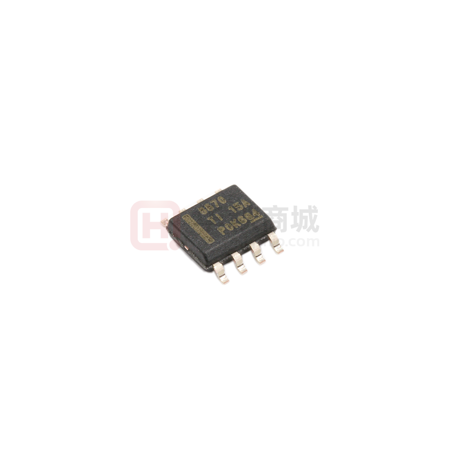
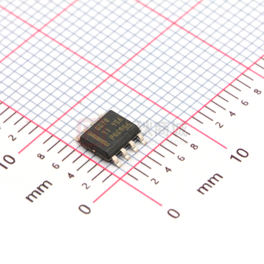
Device Information
PART NUMBER
DRV8870
PACKAGE
HSOP (8)
(1)
BODY SIZE (NOM)
4.90 mm × 6.00 mm
(1) For all available packages, see the orderable addendum at
the end of the data sheet.
H-Bridge States
Simplified Schematic
6.5 to 45 V
DRV8870
3.6 A
IN1
Controller
IN2
BDC
Brushed DC Motor
Driver
VREF
Current
Regulation
ISEN
Fault Protection
Copyright © 2016, Texas Instruments Incorporated
1
An IMPORTANT NOTICE at the end of this data sheet addresses availability, warranty, changes, use in safety-critical applications,
intellectual property matters and other important disclaimers. PRODUCTION DATA.
�DRV8870
SLVSCY8B – AUGUST 2015 – REVISED JULY 2016
www.ti.com
Table of Contents
1
2
3
4
5
6
7
Features ..................................................................
Applications ...........................................................
Description .............................................................
Revision History.....................................................
Pin Configuration and Functions .........................
Specifications.........................................................
1
1
1
2
3
3
6.1
6.2
6.3
6.4
6.5
6.6
3
4
4
4
5
6
Detailed Description .............................................. 7
7.1
7.2
7.3
7.4
8
Absolute Maximum Ratings ......................................
ESD Ratings..............................................................
Recommended Operating Conditions.......................
Thermal Information ..................................................
Electrical Characteristics...........................................
Typical Characteristics ..............................................
Overview ................................................................... 7
Functional Block Diagram ......................................... 7
Feature Description................................................... 8
Device Functional Modes........................................ 10
Application and Implementation ........................ 11
8.1 Application Information............................................ 11
8.2 Typical Application .................................................. 11
9
Power Supply Recommendations...................... 14
9.1 Bulk Capacitance .................................................... 14
10 Layout................................................................... 15
10.1
10.2
10.3
10.4
Layout Guidelines .................................................
Layout Example ....................................................
Thermal Considerations ........................................
Power Dissipation .................................................
15
15
15
15
11 Device and Documentation Support ................. 17
11.1
11.2
11.3
11.4
11.5
11.6
Documentation Support ........................................
Receiving Notification of Documentation Updates
Community Resources..........................................
Trademarks ...........................................................
Electrostatic Discharge Caution ............................
Glossary ................................................................
17
17
17
17
17
17
12 Mechanical, Packaging, and Orderable
Information ........................................................... 17
4 Revision History
NOTE: Page numbers for previous revisions may differ from page numbers in the current version.
Changes from Revision A (January 2016) to Revision B
Page
•
Deleted the power supply voltage ramp rate (VM) parameter from the Absolute Maximum Ratings table .......................... 3
•
Added the output current parameter to the Absolute Maximum Ratings table ...................................................................... 3
•
Added the Receiving Notification of Documentation Updates section ................................................................................ 17
Changes from Original (August 2015) to Revision A
Page
•
Updated the ƒPWM max value and added a note .................................................................................................................... 4
•
Removed the redundant TA condition and added ƒPWM = 24 kHz .......................................................................................... 5
•
Added more information to clarify how the max RMS current varies for different applications ........................................... 12
2
Submit Documentation Feedback
Copyright © 2015–2016, Texas Instruments Incorporated
Product Folder Links: DRV8870
�DRV8870
www.ti.com
SLVSCY8B – AUGUST 2015 – REVISED JULY 2016
5 Pin Configuration and Functions
DDA Package
8-Pin HSOP
Top View
GND
1
IN2
2
8
OUT2
7
ISEN
6
OUT1
5
VM
Thermal
IN1
3
VREF
4
Pad
Pin Functions
PIN
NAME
NO.
TYPE
DESCRIPTION
GND
1
PWR
IN1
3
I
Logic inputs. Controls the H-bridge output. Has internal pulldowns. See Table 1.
IN2
2
I
Logic inputs. Controls the H-bridge output. Has internal pulldowns. See Table 1.
ISEN
7
PWR
OUT1
6
O
H-bridge output. Connect directly to the motor or other inductive load.
OUT2
8
O
H-bridge output. Connect directly to the motor or other inductive load.
VM
5
PWR
VREF
4
I
PAD
Logic ground. Connect to board ground
High-current ground path. If using current regulation, connect ISEN to a resistor (low-value,
high-power-rating) to ground. If not using current regulation, connect ISEN directly to ground.
6.5-V to 45-V power supply. Connect a 0.1-µF bypass capacitor to ground, as well as
sufficient bulk capacitance, rated for the VM voltage.
Analog input. Apply a voltage between 0.3 to 5 V. For information on current regulation, see
the Current Regulation section.
Thermal pad. Connect to board ground. For good thermal dissipation, use large ground
planes on multiple layers, and multiple nearby vias connecting those planes.
—
6 Specifications
6.1 Absolute Maximum Ratings
over operating free-air temperature range (unless otherwise noted) (1)
MIN
MAX
UNIT
Power supply voltage (VM)
–0.3
50
V
Logic input voltage (IN1, IN2)
–0.3
7
V
Reference input pin voltage (VREF)
–0.3
6
V
Continuous phase node pin voltage (OUT1, OUT2)
–0.7
VM + 0.7
V
–0.5
1
V
0
3.5
A
Operating junction temperature, TJ
–40
150
°C
Storage temperature, Tstg
–65
150
°C
Current sense input pin voltage (ISEN)
(2)
Output current (100% duty cycle)
(1)
(2)
Stresses beyond those listed under Absolute Maximum Ratings may cause permanent damage to the device. These are stress ratings
only, which do not imply functional operation of the device at these or any other conditions beyond those indicated under Recommended
Operating Conditions. Exposure to absolute-maximum-rated conditions for extended periods may affect device reliability.
Transients of ±1 V for less than 25 ns are acceptable
Submit Documentation Feedback
Copyright © 2015–2016, Texas Instruments Incorporated
Product Folder Links: DRV8870
3
�DRV8870
SLVSCY8B – AUGUST 2015 – REVISED JULY 2016
www.ti.com
6.2 ESD Ratings
VALUE
V(ESD)
(1)
(2)
Electrostatic discharge
Human-body model (HBM), per ANSI/ESDA/JEDEC JS-001 (1)
±6000
Charged-device model (CDM), per JEDEC specification JESD22-C101 (2)
±750
UNIT
V
JEDEC document JEP155 states that 500-V HBM allows safe manufacturing with a standard ESD control process.
JEDEC document JEP157 states that 250-V CDM allows safe manufacturing with a standard ESD control process.
6.3 Recommended Operating Conditions
over operating free-air temperature range (unless otherwise noted)
MIN
VM
Power supply voltage
VREF
VREF input voltage
VI
NOM
MAX
UNIT
6.5
45
V
0.3 (1)
5
V
Logic input voltage (IN1, IN2)
0
5.5
fPWM
Logic input PWM frequency (IN1, IN2)
0
200 (2)
Ipeak
Peak output current (3)
TA
Operating ambient temperature (3)
(1)
(2)
(3)
V
kHz
0
3.6
A
–40
125
°C
Operational at VREF = 0 to 0.3 V, but accuracy is degraded
The voltages applied to the inputs should have at least 800 ns of pulse width to ensure detection. Typical devices require at least 400
ns. If the PWM frequency is 200 kHz, the usable duty cycle range is 16% to 84%.
Power dissipation and thermal limits must be observed
6.4 Thermal Information
DRV8870
THERMAL METRIC (1)
DDA (HSOP)
UNIT
8 PINS
RθJA
Junction-to-ambient thermal resistance
41.1
°C/W
RθJC(top)
Junction-to-case (top) thermal resistance
53.1
°C/W
RθJB
Junction-to-board thermal resistance
23.1
°C/W
ψJT
Junction-to-top characterization parameter
8.2
°C/W
ψJB
Junction-to-board characterization parameter
23
°C/W
RθJC(bot)
Junction-to-case (bottom) thermal resistance
2.7
°C/W
(1)
4
For more information about traditional and new thermal metrics, see the Semiconductor and IC Package Thermal Metrics application
report.
Submit Documentation Feedback
Copyright © 2015–2016, Texas Instruments Incorporated
Product Folder Links: DRV8870
�DRV8870
www.ti.com
SLVSCY8B – AUGUST 2015 – REVISED JULY 2016
6.5 Electrical Characteristics
TA = 25°C, over recommended operating conditions (unless otherwise noted)
PARAMETER
TEST CONDITIONS
MIN
TYP
MAX
UNIT
POWER SUPPLY (VM)
VM
VM operating voltage
IVM
VM operating supply
current
6.5
VM = 12 V
IVMSLEEP
VM sleep current
VM = 12 V
tON (1)
Turn-on time
VM > VUVLO with IN1 or IN2 high
3
40
45
V
10
mA
10
µA
50
µs
0.5
V
LOGIC-LEVEL INPUTS (IN1, IN2)
VIL
Input logic low voltage
VIH
Input logic high voltage
VHYS
Input logic hysteresis
IIL
Input logic low current
VIN = 0 V
IIH
Input logic high current
VIN = 3.3 V
RPD
Pulldown resistance
to GND
100
tPD
Propagation delay
INx to OUTx change (see Figure 6)
0.7
1
μs
tsleep
Time to sleep
Inputs low to sleep
1
1.5
ms
1.5
V
0.5
–1
V
1
33
μA
100
μA
kΩ
MOTOR DRIVER OUTPUTS (OUT1, OUT2)
RDS(ON)
High-side FET on
resistance
VM = 24 V, I = 1 A, fPWM = 25 kHz
307
360
mΩ
RDS(ON)
Low-side FET on
resistance
VM = 24 V, I = 1 A, fPWM = 25 kHz
258
320
mΩ
tDEAD
Output dead time
Vd
Body diode forward
voltage
220
IOUT = 1 A
ns
0.8
1
10
10.4
V
CURRENT REGULATION
AV
ISEN gain
tOFF
PWM off-time
tBLANK
PWM blanking time
VREF = 2.5 V
9.4
V/V
25
µs
2
µs
PROTECTION CIRCUITS
VUVLO
VM undervoltage lockout
VUV,HYS
VM undervoltage
hysteresis
IOCP
Overcurrent protection trip
level
tOCP
Overcurrent deglitch time
tRETRY
Overcurrent retry time
TSD
Thermal shutdown
temperature
THYS
Thermal shutdown
hysteresis
(1)
VM falls until UVLO triggers
6.1
6.4
VM rises until operation recovers
6.3
6.5
Rising to falling threshold
100
180
3.7
4.5
150
V
mV
6.4
A
1.5
μs
3
ms
175
°C
40
°C
tON applies when the device initially powers up, and when it exits sleep mode.
Submit Documentation Feedback
Copyright © 2015–2016, Texas Instruments Incorporated
Product Folder Links: DRV8870
5
�DRV8870
SLVSCY8B – AUGUST 2015 – REVISED JULY 2016
www.ti.com
6.6 Typical Characteristics
10.5
1.5
1.4
10.25
1.3
A V ( V /V )
N o r m a liz e d R D S ( o n ) / R D S ( o n ) _ 2 5 q C
1.6
1.2
1.1
10
1
9.75
0.9
0.8
0.7
-40
9.5
-20
0
20
40
60
80
100
120
Ambient Temperature (qC)
140
1
1.5
2
2.5
3
VREF (V)
D001
Figure 1. RDS(on) vs Temperature
3.5
4
D003
Figure 2. AV vs VREF
10
IV M S L E E P (µ A )
8
6
4
2
0
0
5
10
15
20
25
30
35
VM (V)
40
45
D004
Figure 3. IVMSLEEP vs VM at 25°C
6
Submit Documentation Feedback
Copyright © 2015–2016, Texas Instruments Incorporated
Product Folder Links: DRV8870
�DRV8870
www.ti.com
SLVSCY8B – AUGUST 2015 – REVISED JULY 2016
7 Detailed Description
7.1 Overview
The DRV8870 device is an optimized 8-pin device for driving brushed DC motors with 6.5 to 45 V and up to 3.6A peak current. The integrated current regulation restricts motor current to a predefined maximum. Two logic
inputs control the H-bridge driver, which consists of four N-channel MOSFETs that have a typical Rds(on) of 565
mΩ (including one high-side and one low-side FET). A single-power input, VM, serves as both device power and
the motor winding bias voltage. The integrated charge pump of the device boosts VM internally and fully
enhances the high-side FETs. Motor speed can be controlled with pulse-width modulation, at frequencies
between 0 to 100 kHz. The device has an integrated sleep mode that is entered by bringing both inputs low. An
assortment of protection features prevent the device from being damaged if a system fault occurs.
7.2 Functional Block Diagram
Power
VM
bulk
VCP
VCP
VM
Charge
Pump
0.1µF
VM
Gate
Driver
OUT1
OCP
GND
PPAD
VCP
IN1
Gate
Driver
Core
Logic
BDC
VM
OUT2
OCP
IN2
ISEN
+
x 10
-
VREF
RSENSE
Protection Features
Overcurrent
Monitoring
Temperature
Sensor
Voltage
Monitoring
Copyright © 2016, Texas Instruments Incorporated
Submit Documentation Feedback
Copyright © 2015–2016, Texas Instruments Incorporated
Product Folder Links: DRV8870
7
�DRV8870
SLVSCY8B – AUGUST 2015 – REVISED JULY 2016
www.ti.com
7.3 Feature Description
7.3.1 Bridge Control
The DRV8870 output consists of four N-channel MOSFETs that are designed to drive high current. These
outputs are controlled by the two logic inputs IN1 and IN2 as listed in Table 1.
Table 1. H-Bridge Control
IN1
IN2
OUT1
OUT2
0
0
High-Z
High-Z
DESCRIPTION
0
1
L
H
Reverse (Current OUT2 → OUT1)
1
0
H
L
Forward (Current OUT1 → OUT2)
1
1
L
L
Brake; low-side slow decay
Coast; H-bridge disabled to High-Z (sleep entered after 1 ms)
The inputs can be set to static voltages for 100% duty cycle drive, or they can be pulse-width modulated (PWM)
for variable motor speed. When using PWM, switching between driving and braking typically works best. For
example, to drive a motor forward with 50% of the maximum RPM, IN1 = 1 and IN2 = 0 during the driving period,
and IN1 = 1 and IN2 = 1 during the other period. Alternatively, the coast mode (IN1 = 0, IN2 = 0) for fast current
decay is also available. The input pins can be powered before VM is applied.
VM
VM
1 Reverse drive
1 Forward drive
2 Slow decay (brake)
2 Slow decay (brake)
1
1
OUT1
3 High-Z (coast)
3 High-Z (coast)
OUT2
OUT1
OUT2
2
2
3
3
FORWARD
REVERSE
Figure 4. H-Bridge Current Paths
7.3.2 Sleep Mode
When the IN1 and IN2 pins are both low for time tSLEEP (typically 1 ms), the DRV8870 device enters a low-power
sleep mode, where the outputs remain High-Z and the device uses IVMSLEEP (µA) of current. If the device is
powered up while both inputs are low, it immediately enters sleep mode. After the IN1 or IN2 pins are high for at
least 5 µs, the device is operational 50 µs (tON) later.
7.3.3 Current Regulation
The DRV8870 device limits the output current based on the analog input, VREF, and the resistance of an
external sense resistor on the ISEN pin according to Equation 1:
8
Submit Documentation Feedback
Copyright © 2015–2016, Texas Instruments Incorporated
Product Folder Links: DRV8870
�DRV8870
www.ti.com
ITRIP (A)
SLVSCY8B – AUGUST 2015 – REVISED JULY 2016
VREF (V)
A v u RISEN (:)
VREF (V)
10 u RISEN (:)
(1)
For example, if VREF = 3.3 V and a RISEN = 0.15 Ω, the DRV8870 device limits motor current to 2.2 A no matter
how much load torque is applied. For guidelines on selecting a sense resistor, see the Sense Resistor section.
When ITRIP is reached, the device enforces slow current decay by enabling both low-side FETs, and it does this
for a time of tOFF (typically 25 µs).
Motor Current (A)
ITRIP
tBLANK
tDRIVE
tOFF
Figure 5. Current-Regulation Time Periods
After tOFF elapses, the output is re-enabled according to the two inputs, INx. The drive time (tDRIVE) until reaching
another ITRIP event heavily depends on the VM voltage, the back-EMF of the motor, and the inductance of the
motor.
7.3.4 Dead Time
When an output changes from driving high to driving low, or driving low to driving high, dead time is automatically
inserted to prevent shoot-through. The tDEAD time is the time in the middle when the output is High-Z. If the
output pin is measured during tDEAD, the voltage depends on the direction of current. If the current is leaving the
pin, the voltage is a diode drop below ground. If the current is entering the pin, the voltage is a diode drop above
VM. This diode is the body diode of the high-side or low-side FET.
IN1
IN2
OUT1
tPD
tR
tDEAD
tPD
tF
tDEAD
tPD
tF
tDEAD
tPD
tR
tDEAD
OUT2
Figure 6. Propagation Delay Time
Submit Documentation Feedback
Copyright © 2015–2016, Texas Instruments Incorporated
Product Folder Links: DRV8870
9
�DRV8870
SLVSCY8B – AUGUST 2015 – REVISED JULY 2016
www.ti.com
7.3.5 Protection Circuits
The DRV8870 device is fully protected against VM undervoltage, overcurrent, and overtemperature events.
7.3.5.1 VM Undervoltage Lockout (UVLO)
If at any time the voltage on the VM pin falls below the undervoltage-lockout threshold voltage, all FETs in the Hbridge will be disabled. Operation resumes when VM rises above the UVLO threshold.
7.3.5.2 Overcurrent Protection (OCP)
If the output current exceeds the OCP threshold, IOCP, for longer than tOCP, all FETs in the H-bridge are disabled
for a duration of tRETRY. After that, the H-bridge is re-enabled according to the state of the INx pins. If the
overcurrent fault is still present, the cycle repeats; otherwise normal device operation resumes.
7.3.5.3 Thermal Shutdown (TSD)
If the die temperature exceeds safe limits, all FETs in the H-bridge are disabled. After the die temperature has
fallen to a safe level, operation automatically resumes.
Table 2. Protection Functionality
FAULT
CONDITION
H-BRIDGE BECOMES
RECOVERY
VM undervoltage lockout (UVLO)
VM < VUVLO
Disabled
VM > VUVLO
Overcurrent (OCP)
IOUT > IOCP
Disabled
tRETRY
Thermal Shutdown (TSD)
TJ > 150°C
Disabled
TJ < TSD – THYS
7.4 Device Functional Modes
The DRV8870 device can be used in multiple ways to drive a brushed DC motor.
7.4.1 PWM With Current Regulation
This scheme uses all of the capabilities of the device. The ITRIP current is set above the normal operating current,
and high enough to achieve an adequate spin-up time, but low enough to constrain current to a desired level.
Motor speed is controlled by the duty cycle of one of the inputs, while the other input is static. Brake or slow
decay is typically used during the off-time.
7.4.2 PWM Without Current Regulation
If current regulation is not required, the ISEN pin should be directly connected to the PCB ground plane. The
VREF voltage must still be 0.3 to 5 V, and larger voltages provide greater noise margin. This mode provides the
highest-possible peak current which is up to 3.6 A for a few hundred milliseconds (depending on PCB
characteristics and the ambient temperature). If current exceeds 3.6 A, the device might reach overcurrent
protection (OCP) or overtemperature shutdown (TSD). If that happens, the device disables and protects itself for
about 3 ms (tRETRY) and then resumes normal operation.
7.4.3 Static Inputs With Current Regulation
The IN1 and IN2 pins can be set high and low for 100% duty cycle drive, and ITRIP can be used to control the
current of the motor, speed, and torque capability.
7.4.4 VM Control
In some systems, varying VM as a means of changing motor speed is desirable. See the Motor Voltage section
for more information.
10
Submit Documentation Feedback
Copyright © 2015–2016, Texas Instruments Incorporated
Product Folder Links: DRV8870
�DRV8870
www.ti.com
SLVSCY8B – AUGUST 2015 – REVISED JULY 2016
8 Application and Implementation
NOTE
Information in the following applications sections is not part of the TI component
specification, and TI does not warrant its accuracy or completeness. TI’s customers are
responsible for determining suitability of components for their purposes. Customers should
validate and test their design implementation to confirm system functionality.
8.1 Application Information
The DRV8870 device is typically used to drive one brushed DC motor.
8.2 Typical Application
OUT2
GND
3.3 V
Controller
IN1
0.2 Ÿ
ISEN
IN2
DRV8870
BDC
OUT1
3.3 V
VM
VREF
PPAD
0.1 µF
47 µF
+
±
6.5 to 45 V
Power Supply
Copyright © 2016, Texas Instruments Incorporated
Figure 7. Typical Connections
8.2.1 Design Requirements
Table 3 lists the design parameters.
Table 3. Design Parameters
DESIGN PARAMETER
Motor voltage
Motor RMS current
Motor startup current
Motor current trip point
REFERENCE
EXAMPLE VALUE
VM
24 V
IRMS
0.8 A
ISTART
2A
ITRIP
2.2 A
VREF voltage
VREF
3.3 V
Sense resistance
RISEN
0.15 Ω
PWM frequency
fPWM
5 kHz
8.2.2 Detailed Design Procedure
8.2.2.1 Motor Voltage
The motor voltage to use depends on the ratings of the motor selected and the desired RPM. A higher voltage
spins a brushed DC motor faster with the same PWM duty cycle applied to the power FETs. A higher voltage
also increases the rate of current change through the inductive motor windings.
8.2.2.2 Drive Current
The current path is through the high-side sourcing DMOS power driver, motor winding, and low-side sinking
DMOS power driver. Power dissipation losses in one source and sink DMOS power driver are shown in
Equation 2.
Submit Documentation Feedback
Copyright © 2015–2016, Texas Instruments Incorporated
Product Folder Links: DRV8870
11
�DRV8870
SLVSCY8B – AUGUST 2015 – REVISED JULY 2016
PD
I2 RDS(on)Source
www.ti.com
RDS(on)Sink
(2)
The DRV8870 device has been measured to be capable of 2-A RMS current at 25°C on standard FR-4 PCBs.
The maximum RMS current varies based on the PCB design, ambient temperature, and PWM frequency.
Typically, switching the inputs at 200 kHz compared to 20 kHz causes 20% more power loss in heat.
8.2.2.3 Sense Resistor
For optimal performance, the sense resistor must have the following characteristics:
• Surface-mount
• Low inductance
• Rated for high enough power
• Placed closely to the motor driver
The power dissipated by the sense resistor equals IRMS2 × R. For example, if peak motor current is 3 A, RMS
motor current is 1.5 A, and a 0.2-Ω sense resistor is used, the resistor dissipates 1.5 A2 × 0.2 Ω = 0.45 W. The
power quickly increases with higher current levels.
Resistors typically have a rated power within some ambient temperature range, along with a derated power curve
for high ambient temperatures. When a PCB is shared with other components generating heat, the system
designer should add margin. Measuring the actual sense resistor temperature in a final system is always best.
Because power resistors are larger and more expensive than standard resistors, using multiple standard
resistors in parallel, between the sense node and ground, is common and distributes the current and heat
dissipation.
8.2.3 Application Curves
Figure 8. Current Ramp With a 2-Ω, 1 mH,
RL Load and VM = 12 V
12
Submit Documentation Feedback
Figure 9. Current Ramp With a 2-Ω, 1 mH,
RL Load and VM = 24 V
Copyright © 2015–2016, Texas Instruments Incorporated
Product Folder Links: DRV8870
�DRV8870
www.ti.com
SLVSCY8B – AUGUST 2015 – REVISED JULY 2016
Figure 10. Current Ramp With a 2-Ω, 1 mH,
RL Load and VM = 45 V
Figure 11. tPD
Figure 12. Current Regulation With VREF = 2 V and
150 mΩ
Figure 13. OCP With 45 V and the Outputs Shorted
Together
Submit Documentation Feedback
Copyright © 2015–2016, Texas Instruments Incorporated
Product Folder Links: DRV8870
13
�DRV8870
SLVSCY8B – AUGUST 2015 – REVISED JULY 2016
www.ti.com
9 Power Supply Recommendations
9.1 Bulk Capacitance
Having appropriate local bulk capacitance is an important factor in motor drive system design. Having more bulk
capacitance is generally beneficial, while the disadvantages are increased cost and physical size.
The amount of local capacitance needed depends on a variety of factors, including:
• The highest current required by the motor system
• The capacitance of the power supply and ability to source current
• The amount of parasitic inductance between the power supply and motor system
• The acceptable voltage ripple
• The type of motor used (brushed DC, brushless DC, stepper)
• The motor braking method
The inductance between the power supply and motor drive system limits how the rate current can change from
the power supply. If the local bulk capacitance is too small, the system responds to excessive current demands
or dumps from the motor with a change in voltage. When adequate bulk capacitance is used, the motor voltage
remains stable and high current can be quickly supplied.
The data sheet generally provides a recommended value, but system-level testing is required to determine the
appropriate sized bulk capacitor.
Power Supply
Parasitic Wire
Inductance
Motor Drive System
VBB
+
±
+
Motor
Driver
GND
Local
Bulk Capacitor
IC Bypass
Capacitor
Figure 14. Example Setup of Motor Drive System With External Power Supply
The voltage rating for bulk capacitors should be higher than the operating voltage, to provide margin for cases
when the motor transfers energy to the supply.
14
Submit Documentation Feedback
Copyright © 2015–2016, Texas Instruments Incorporated
Product Folder Links: DRV8870
�DRV8870
www.ti.com
SLVSCY8B – AUGUST 2015 – REVISED JULY 2016
10 Layout
10.1 Layout Guidelines
The bulk capacitor should be placed to minimize the distance of the high-current path through the motor driver
device. The connecting metal trace widths should be as wide as possible, and numerous vias should be used
when connecting PCB layers. These practices minimize inductance and allow the bulk capacitor to deliver high
current.
Small-value capacitors should be ceramic, and placed closely to device pins.
The high-current device outputs should use wide metal traces.
The device thermal pad should be soldered to the PCB top-layer ground plane. Multiple vias should be used to
connect to a large bottom-layer ground plane. The use of large metal planes and multiple vias help dissipate the
I² x RDS(on) heat that is generated in the device.
10.2 Layout Example
Figure 15 shows the recommended layout and component placement.
GND
OUT2
IN2
ISEN
IN1
OUT1
VREF
VM
+
Figure 15. Layout Recommendation
10.3 Thermal Considerations
The DRV8870 device has thermal shutdown (TSD) as described in the Thermal Shutdown (TSD) section. If the
die temperature exceeds approximately 175°C, the device is disabled until the temperature drops below the
temperature hysteresis level.
Any tendency of the device to enter TSD is an indication of either excessive power dissipation, insufficient
heatsinking, or too high of an ambient temperature.
10.4 Power Dissipation
Power dissipation in the DRV8870 device is dominated by the power dissipated in the output FET resistance,
RDS(on). Use the equation in the Drive Current section to calculate the estimated average power dissipation when
driving a load.
Note that at startup, the current is much higher than normal running current; this peak current and its duration
must be also be considered.
Submit Documentation Feedback
Copyright © 2015–2016, Texas Instruments Incorporated
Product Folder Links: DRV8870
15
�DRV8870
SLVSCY8B – AUGUST 2015 – REVISED JULY 2016
www.ti.com
Power Dissipation (continued)
The maximum amount of power that can be dissipated in the device is dependent on ambient temperature and
heatsinking.
NOTE
RDS(on) increases with temperature, so as the device heats, the power dissipation
increases. This fact must be taken into consideration when sizing the heatsink.
The power dissipation of the DRV8870 device is a function of RMS motor current and the FET resistance
(RDS(ON)) of each output.
Power | IRMS2 u High-side RDS(ON)
Low-side RDS(ON)
(3)
For this example, the ambient temperature is 58°C, and the junction temperature reaches 80°C. At 58°C, the
sum of RDS(ON) is about 0.72 Ω. With an example motor current of 0.8 A, the dissipated power in the form of heat
is 0.8 A2 × 0.72 Ω = 0.46 W.
The temperature that the DRV8870 reaches will depend on the thermal resistance to the air and PCB. It is
important to solder the device PowerPAD to the PCB ground plane, with vias to the top and bottom board layers,
in order dissipate heat into the PCB and reduce the device temperature. In the example used here, the DRV8870
device had an effective thermal resistance RθJA of 48°C/W, and:
TJ TA (PD u RTJA ) 58qC (0.46 W u 48qC/W ) 80qC
(4)
10.4.1 Heatsinking
The PowerPAD package uses an exposed pad to remove heat from the device. For proper operation, this pad
must be thermally connected to copper on the PCB to dissipate heat. On a multi-layer PCB with a ground plane,
this connection can be accomplished by adding a number of vias to connect the thermal pad to the ground plane.
On PCBs without internal planes, a copper area can be added on either side of the PCB to dissipate heat. If the
copper area is on the opposite side of the PCB from the device, thermal vias are used to transfer the heat
between top and bottom layers.
For details about how to design the PCB, refer to PowerPAD™ Thermally Enhanced Package and PowerPAD
Made Easy™, available at www.ti.com. In general, the more copper area that can be provided, the more power
can be dissipated.
16
Submit Documentation Feedback
Copyright © 2015–2016, Texas Instruments Incorporated
Product Folder Links: DRV8870
�DRV8870
www.ti.com
SLVSCY8B – AUGUST 2015 – REVISED JULY 2016
11 Device and Documentation Support
11.1 Documentation Support
11.1.1 Related Documentation
For related documentation, see the following:
• Calculating Motor Driver Power Dissipation
• Current Recirculation and Decay Modes
• PowerPAD™ Made Easy
• PowerPAD™ Thermally Enhanced Package
• Understanding Motor Driver Current Ratings
11.2 Receiving Notification of Documentation Updates
To receive notification of documentation updates, navigate to the device product folder on ti.com. In the upper
right corner, click on Alert me to register and receive a weekly digest of any product information that has
changed. For change details, review the revision history included in any revised document.
11.3 Community Resources
The following links connect to TI community resources. Linked contents are provided "AS IS" by the respective
contributors. They do not constitute TI specifications and do not necessarily reflect TI's views; see TI's Terms of
Use.
TI E2E™ Online Community TI's Engineer-to-Engineer (E2E) Community. Created to foster collaboration
among engineers. At e2e.ti.com, you can ask questions, share knowledge, explore ideas and help
solve problems with fellow engineers.
Design Support TI's Design Support Quickly find helpful E2E forums along with design support tools and
contact information for technical support.
11.4 Trademarks
PowerPAD, E2E are trademarks of Texas Instruments.
All other trademarks are the property of their respective owners.
11.5 Electrostatic Discharge Caution
These devices have limited built-in ESD protection. The leads should be shorted together or the device placed in conductive foam
during storage or handling to prevent electrostatic damage to the MOS gates.
11.6 Glossary
SLYZ022 — TI Glossary.
This glossary lists and explains terms, acronyms, and definitions.
12 Mechanical, Packaging, and Orderable Information
The following pages include mechanical, packaging, and orderable information. This information is the most
current data available for the designated devices. This data is subject to change without notice and revision of
this document. For browser-based versions of this data sheet, refer to the left-hand navigation.
Submit Documentation Feedback
Copyright © 2015–2016, Texas Instruments Incorporated
Product Folder Links: DRV8870
17
�PACKAGE OPTION ADDENDUM
www.ti.com
26-May-2016
PACKAGING INFORMATION
Orderable Device
Status
(1)
Package Type Package Pins Package
Drawing
Qty
Eco Plan
Lead/Ball Finish
MSL Peak Temp
(2)
(6)
(3)
Op Temp (°C)
Device Marking
(4/5)
DRV8870DDA
ACTIVE SO PowerPAD
DDA
8
75
Green (RoHS
& no Sb/Br)
CU NIPDAUAG
Level-2-260C-1 YEAR
-40 to 125
8870
DRV8870DDAR
ACTIVE SO PowerPAD
DDA
8
2500
Green (RoHS
& no Sb/Br)
CU NIPDAUAG
Level-2-260C-1 YEAR
-40 to 125
8870
(1)
The marketing status values are defined as follows:
ACTIVE: Product device recommended for new designs.
LIFEBUY: TI has announced that the device will be discontinued, and a lifetime-buy period is in effect.
NRND: Not recommended for new designs. Device is in production to support existing customers, but TI does not recommend using this part in a new design.
PREVIEW: Device has been announced but is not in production. Samples may or may not be available.
OBSOLETE: TI has discontinued the production of the device.
(2)
Eco Plan - The planned eco-friendly classification: Pb-Free (RoHS), Pb-Free (RoHS Exempt), or Green (RoHS & no Sb/Br) - please check http://www.ti.com/productcontent for the latest availability
information and additional product content details.
TBD: The Pb-Free/Green conversion plan has not been defined.
Pb-Free (RoHS): TI's terms "Lead-Free" or "Pb-Free" mean semiconductor products that are compatible with the current RoHS requirements for all 6 substances, including the requirement that
lead not exceed 0.1% by weight in homogeneous materials. Where designed to be soldered at high temperatures, TI Pb-Free products are suitable for use in specified lead-free processes.
Pb-Free (RoHS Exempt): This component has a RoHS exemption for either 1) lead-based flip-chip solder bumps used between the die and package, or 2) lead-based die adhesive used between
the die and leadframe. The component is otherwise considered Pb-Free (RoHS compatible) as defined above.
Green (RoHS & no Sb/Br): TI defines "Green" to mean Pb-Free (RoHS compatible), and free of Bromine (Br) and Antimony (Sb) based flame retardants (Br or Sb do not exceed 0.1% by weight
in homogeneous material)
(3)
MSL, Peak Temp. - The Moisture Sensitivity Level rating according to the JEDEC industry standard classifications, and peak solder temperature.
(4)
There may be additional marking, which relates to the logo, the lot trace code information, or the environmental category on the device.
(5)
Multiple Device Markings will be inside parentheses. Only one Device Marking contained in parentheses and separated by a "~" will appear on a device. If a line is indented then it is a continuation
of the previous line and the two combined represent the entire Device Marking for that device.
(6)
Lead/Ball Finish - Orderable Devices may have multiple material finish options. Finish options are separated by a vertical ruled line. Lead/Ball Finish values may wrap to two lines if the finish
value exceeds the maximum column width.
Important Information and Disclaimer:The information provided on this page represents TI's knowledge and belief as of the date that it is provided. TI bases its knowledge and belief on information
provided by third parties, and makes no representation or warranty as to the accuracy of such information. Efforts are underway to better integrate information from third parties. TI has taken and
continues to take reasonable steps to provide representative and accurate information but may not have conducted destructive testing or chemical analysis on incoming materials and chemicals.
TI and TI suppliers consider certain information to be proprietary, and thus CAS numbers and other limited information may not be available for release.
Addendum-Page 1
Samples
�PACKAGE OPTION ADDENDUM
www.ti.com
26-May-2016
In no event shall TI's liability arising out of such information exceed the total purchase price of the TI part(s) at issue in this document sold by TI to Customer on an annual basis.
Addendum-Page 2
�PACKAGE MATERIALS INFORMATION
www.ti.com
26-May-2016
TAPE AND REEL INFORMATION
*All dimensions are nominal
Device
DRV8870DDAR
Package Package Pins
Type Drawing
SO
Power
PAD
DDA
8
SPQ
Reel
Reel
A0
Diameter Width (mm)
(mm) W1 (mm)
2500
330.0
12.8
Pack Materials-Page 1
6.4
B0
(mm)
K0
(mm)
P1
(mm)
5.2
2.1
8.0
W
Pin1
(mm) Quadrant
12.0
Q1
�PACKAGE MATERIALS INFORMATION
www.ti.com
26-May-2016
*All dimensions are nominal
Device
Package Type
Package Drawing
Pins
SPQ
Length (mm)
Width (mm)
Height (mm)
DRV8870DDAR
SO PowerPAD
DDA
8
2500
366.0
364.0
50.0
Pack Materials-Page 2
�GENERIC PACKAGE VIEW
DDA 8
PowerPAD TM SOIC - 1.7 mm max height
PLASTIC SMALL OUTLINE
Images above are just a representation of the package family, actual package may vary.
Refer to the product data sheet for package details.
4202561/G
����IMPORTANT NOTICE AND DISCLAIMER
TI PROVIDES TECHNICAL AND RELIABILITY DATA (INCLUDING DATASHEETS), DESIGN RESOURCES (INCLUDING REFERENCE
DESIGNS), APPLICATION OR OTHER DESIGN ADVICE, WEB TOOLS, SAFETY INFORMATION, AND OTHER RESOURCES “AS IS”
AND WITH ALL FAULTS, AND DISCLAIMS ALL WARRANTIES, EXPRESS AND IMPLIED, INCLUDING WITHOUT LIMITATION ANY
IMPLIED WARRANTIES OF MERCHANTABILITY, FITNESS FOR A PARTICULAR PURPOSE OR NON-INFRINGEMENT OF THIRD
PARTY INTELLECTUAL PROPERTY RIGHTS.
These resources are intended for skilled developers designing with TI products. You are solely responsible for (1) selecting the appropriate
TI products for your application, (2) designing, validating and testing your application, and (3) ensuring your application meets applicable
standards, and any other safety, security, or other requirements. These resources are subject to change without notice. TI grants you
permission to use these resources only for development of an application that uses the TI products described in the resource. Other
reproduction and display of these resources is prohibited. No license is granted to any other TI intellectual property right or to any third
party intellectual property right. TI disclaims responsibility for, and you will fully indemnify TI and its representatives against, any claims,
damages, costs, losses, and liabilities arising out of your use of these resources.
TI’s products are provided subject to TI’s Terms of Sale (www.ti.com/legal/termsofsale.html) or other applicable terms available either on
ti.com or provided in conjunction with such TI products. TI’s provision of these resources does not expand or otherwise alter TI’s applicable
warranties or warranty disclaimers for TI products.
Mailing Address: Texas Instruments, Post Office Box 655303, Dallas, Texas 75265
Copyright © 2019, Texas Instruments Incorporated
�


 工商网监
湘ICP备2023018690号
工商网监
湘ICP备2023018690号

