Product
Folder
Order
Now
Technical
Documents
Support &
Community
Tools &
Software
DS110DF1610
SNLS472A – JANUARY 2014 – REVISED JUNE 2017
DS110DF1610 8.5- to 11.3-Gbps 16-Channel Retimer
1 Features
2 Description
•
The DS110DF1610 is a sixteen-channel multi-rate
retimer with integrated signal conditioning. The device
includes a full adaptive Continuous Time Linear
Equalizer (CTLE), Decision Feedback Equalizer
(DFE), clock and data recovery (CDR), and a transmit
FIR filter to enhance the reach and robustness over
long, lossy, crosstalk impaired high speed serial links
to achieve BER < 1×10-15.
1
•
•
•
•
•
•
•
•
•
•
•
•
•
•
•
•
Pin-Compatible Family
– DS150DF1610: 12.5 - 15G
– DS125DF1610: 9.8 to 12.5G
– DS110DF1610: 8.5 – 11.3G
4x4 Analog Cross Point Switch for Each Quad
Fully-Adaptive CTLE
Self-Tuning DFE, With Optional Continuous
Adaption
On-Chip, AC-coupling on Receive Inputs
Adjustable Transmit VOD
Adjustable 3-Tap Transmit FIR Filter
Locks to Half/Quarter/Eighth Data Rates For
Legacy Support
On-Chip Eye Monitor (EOM), PRBS Checker,
PRBS Pattern Generator
Supports IEEE 1149.1 and 1149.6
Programmable Output Polarity Inversion
Input Signal Detection, CDR Lock Detection
Single 2.5-V ±5% Power Supply
SMBus-Based Register Configuration
Optional EEPROM Configuration
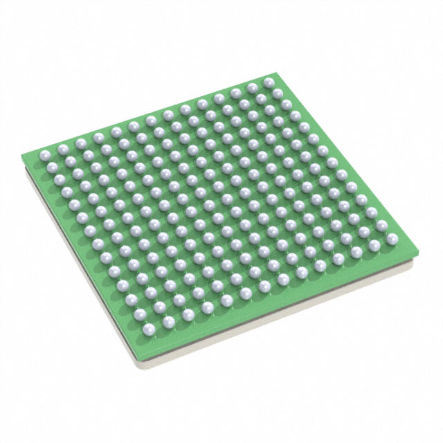
15-mm × 15-mm, 196-Pin FCBGA Package
Operating Temp Range : –10°C to +85°C
Typical Application Diagram
Each channel of the DS110DF1610 independently
locks to serial data at 8.5 to 11.3 Gbps and any
supported sub-multiple. A simple external oscillator
(±100ppm) that is synchronous or asynchronous with
the incoming data stream can be used as a reference
clock to speed up the lock process. Integrated 4x4
cross point switches allow for full non-blocking routing
or broadcasting within each quad of the
DS110DF1610.
Programmable transmit FIR filter offers control of the
pre-cursor, main tap and post-cursor for transmit
equalization. The fully adaptive receive equalization
(CTLE and DFE) enables longer distance
transmission in lossy copper interconnects and
backplanes with multiple connectors.
A non-disruptive mission mode eye-monitor feature
allows link monitoring internal to the receiver. The
built-in PRBS generator and checker compliment the
internal diagnostic features to complete standalone
BERT measurements. Built-in JTAG enables
manufacturing tests.
Device Information(1)
PART NUMBER
DS110DF1610
PACKAGE
FCBGA (196)
BODY SIZE (NOM)
15.00 mm × 15.00 mm
(1) For all available packages, see the orderable addendum at
the end of the data sheet.
Copyright © 2017, Texas Instruments Incorporated
1
An IMPORTANT NOTICE at the end of this data sheet addresses availability, warranty, changes, use in safety-critical applications,
intellectual property matters and other important disclaimers. PRODUCTION DATA.
�DS110DF1610
SNLS472A – JANUARY 2014 – REVISED JUNE 2017
www.ti.com
Table of Contents
1
2
3
4
5
6
Features ..................................................................
Description .............................................................
Revision History.....................................................
Pin Configuration and Functions .........................
Specifications.........................................................
1
1
2
3
8
5.1
5.2
5.3
5.4
8
8
8
9
Absolute Maximum Ratings (DS110DF1610) ..........
Recommended Operating Conditions.......................
Thermal Characteristics ............................................
Electrical Characteristics...........................................
Detailed Description ............................................ 12
6.1
6.2
6.3
6.4
6.5
6.6
7
Overview .................................................................
Functional Block Diagrams .....................................
Feature Description.................................................
Device Functional Modes........................................
Programming ..........................................................
Register Maps .........................................................
12
12
13
21
22
23
Application and Implementation ........................ 66
7.1 Typical Applications ................................................ 66
7.2 Initialization Setup ................................................... 67
8
Power Supply Recommendations...................... 71
8.1 Power Supply Filtering ............................................ 71
3 Revision History
NOTE: Page numbers for previous revisions may differ from page numbers in the current version.
Changes from Original (January 2014) to Revision A
•
2
Page
Changed device status from PRODUCT PREVIEW to PRODUCTION DATA ...................................................................... 1
Submit Documentation Feedback
Copyright © 2014–2017, Texas Instruments Incorporated
Product Folder Links: DS110DF1610
�DS110DF1610
www.ti.com
SNLS472A – JANUARY 2014 – REVISED JUNE 2017
4 Pin Configuration and Functions
P
N
M
L
01
02
TX_6B_N
TX_6B_P
GND
GND
GND
GND
TX_5B_N
03
04
05
06
TX_7A_N
TX_7A_P
GND
07
08
09
10
REF_CLK
_P
11
12
13
14
K
J
H
G
F
E
D
C
B
A
TX_4B_N
TX_4B_P
GND
GND
TX_3A_N
TX_3A_P
GND
GND
TX_1A_N
TX_1A_P
TX_5B_P
GND
GND
TX_4A_N
TX_4A_P
GND
GND
TX_2A_N
TX_2A_P
GND
GND
GND
GND
TX_5A_N
TX_5A_P
GND
GND
TX_2B_N
TX_2B_P
GND
GND
TX_0B_N
TX_0B_P
GND
TX_6A_N
TX_6A_P
GND
GND
TX_3B_N
TX_3B_P
GND
GND
TX_1B_N
TX_1B_P
GND
GND
TX_7B_N
TX_7B_P
GND
ALL_DON
E
VDD
VDD
GND
READ_E
N
VDD
VDD
ADDR1
GND
TX_0A_N
TX_0A_P
GND
GND
N/C
SCL_IO
VDD
GND
VDD
GND
VDD
GND
TCK_IO
N/C
ADDR0
GND
TMS_IO
CLK_MO
N_P
N/C
SDA_IO
N/C
REF_CLK
_N
EN_SMB
INTERR#
_IO
RESET#_
IO
VDD
GND
VDD
GND
VDD
GND
N/C
TRST_IO
N/C
CLK_MO
N_N
GND
GND
N/C
N/C
GND
VDD
GND
VDD
GND
VDD
N/C
N/C
GND
GND
RX_7B_N
RX_7B_P
GND
GND
VDD
VDD
GND
GND
VDD
VDD
GND
GND
RX_0A_N
RX_0A_P
GND
GND
RX_6A_N
RX_6A_P
GND
GND
RX_3B_N
RX_3B_P
GND
GND
RX_1B_N
RX_1B_P
GND
GND
RX_7A_N
RX_7A_P
GND
GND
RX_5A_N
RX_5A_P
GND
GND
RX_2B_N
RX_2B_P
GND
GND
RX_0B_N
RX_0B_P
GND
GND
RX_5B_N
RX_5B_P
GND
GND
RX_4A_N
RX_4A_P
GND
GND
RX_2A_N
RX_2A_P
GND
GND
RX_6B_N
RX_6B_P
GND
GND
RX_4B_N
RX_4B_P
GND
GND
RX_3A_N
RX_3A_P
GND
GND
RX_1A_N
RX_1A_P
P
N
J
H
G
F
E
D
C
B
A
M
L
GND
VDD
K
GND
VDD
GND
VDD
TDI_IO
TDO_IO
01
02
03
04
05
06
07
08
09
10
11
12
13
14
(TOP VIEW)
Pin Descriptions
DS110DF1610,
DS125DF1610 PIN NAME
DS150DF1610 PIN
NAME
NO.
I/O TYPE
DESCRIPTION
HIGH-SPEED DIFFERENTIAL I/Os
RX_1A_P
RX_1A_N
RX_0_0P
RX_0_0N
A14
B14
I, CML
Inverting and non-inverting CMLcompatible, AC coupled differential
inputs. An on-chip 100 Ohm differential
termination resistor connects these
inputs.
RX_0B_P
Rx_0B_N
RX_0_1P
RX_0_1N
A12
B12
I, CML
Inverting and non-inverting CMLcompatible, AC coupled differential
inputs. An on-chip 100 Ohm differential
termination resistor connects these
inputs.
RX_0A_P
RX_0A_N
RX_0_2P
RX_0_2N
A10
B10
I, CML
Inverting and non-inverting CMLcompatible, AC coupled differential
inputs. An on-chip 100 Ohm differential
termination resistor connects these
inputs.
RX_2A_P
RX_2A_N
RX_0_3P
RX_0_3N
C13
D13
I, CML
Inverting and non-inverting CMLcompatible, AC coupled differential
inputs. An on-chip 100 Ohm differential
termination resistor connects these
inputs.
RX_1B_P
RX_1B_N
RX_0_4P
RX_0_4N
C11
D11
I, CML
Inverting and non-inverting CMLcompatible, AC coupled differential
inputs. An on-chip 100 Ohm differential
termination resistor connects these
inputs.
Submit Documentation Feedback
Copyright © 2014–2017, Texas Instruments Incorporated
Product Folder Links: DS110DF1610
3
�DS110DF1610
SNLS472A – JANUARY 2014 – REVISED JUNE 2017
www.ti.com
Pin Descriptions (continued)
DS110DF1610,
DS125DF1610 PIN NAME
DS150DF1610 PIN
NAME
NO.
I/O TYPE
DESCRIPTION
RX_3A_P
RX_3A_N
RX_0_5P
RX_0_5N
E14
F14
I, CML
Inverting and non-inverting CMLcompatible, AC coupled differential
inputs. An on-chip 100 Ohm differential
termination resistor connects these
inputs.
RX_2B_P
RX_2B_N
RX_0_6P
RX_0_6N
E12
F12
I, CML
Inverting and non-inverting CMLcompatible, AC coupled differential
inputs. An on-chip 100 Ohm differential
termination resistor connects these
inputs.
RX_4A_P
RX_4A_N
RX_0_7P
RX_0_7N
G13
H13
I, CML
Inverting and non-inverting CMLcompatible, AC coupled differential
inputs. An on-chip 100 Ohm differential
termination resistor connects these
inputs.
RX_3B_P
RX_3B_N
RX_1_0P
RX_1_0N
G11
H11
I, CML
Inverting and non-inverting CMLcompatible, AC coupled differential
inputs. An on-chip 100 Ohm differential
termination resistor connects these
inputs.
RX_4B_P
Rx_4B_N
RX_1_1P
RX_1_1N
J14
K14
I, CML
Inverting and non-inverting CMLcompatible, AC coupled differential
inputs. An on-chip 100 Ohm differential
termination resistor connects these
inputs.
RX_5A_P
RX_5A_N
RX_1_2P
RX_1_2N
J12
K12
I, CML
Inverting and non-inverting CMLcompatible, AC coupled differential
inputs. An on-chip 100 Ohm differential
termination resistor connects these
inputs.
RX_5B_P
RX_5B_N
RX_1_3P
RX_1_3N
L13
M13
I, CML
Inverting and non-inverting CMLcompatible, AC coupled differential
inputs. An on-chip 100 Ohm differential
termination resistor connects these
inputs.
RX_6A_P
RX_6A_N
RX_1_4P
RX_1_4N
L11
M11
I, CML
Inverting and non-inverting CMLcompatible, AC coupled differential
inputs. An on-chip 100 Ohm differential
termination resistor connects these
inputs.
RX_6B_P
RX_6B_N
RX_1_5P
RX_1_5N
N14
P14
I, CML
Inverting and non-inverting CMLcompatible, AC coupled differential
inputs. An on-chip 100 Ohm differential
termination resistor connects these
inputs.
RX_7A_P
RX_7A_N
RX_1_6P
RX_1_6N
N12
P12
I, CML
Inverting and non-inverting CMLcompatible, AC coupled differential
inputs. An on-chip 100 Ohm differential
termination resistor connects these
inputs.
RX_7B_P
RX_7B_N
RX_1_7P
RX_1_7N
N10
P10
I, CML
Inverting and non-inverting CMLcompatible, AC coupled differential
inputs. An on-chip 100 Ohm differential
termination resistor connects these
inputs.
TX_1A_P
TX_1A_N
TX_0_0P
TX_0_0N
A1
B1
O, CML
Inverting and non-inverting CMLcompatible differential outputs. Driver
presents an output impedance of 100
ohms between these outputs when
switching.
4
Submit Documentation Feedback
Copyright © 2014–2017, Texas Instruments Incorporated
Product Folder Links: DS110DF1610
�DS110DF1610
www.ti.com
SNLS472A – JANUARY 2014 – REVISED JUNE 2017
Pin Descriptions (continued)
DS110DF1610,
DS125DF1610 PIN NAME
DS150DF1610 PIN
NAME
NO.
I/O TYPE
DESCRIPTION
TX_0B_P
TX_0B_N
TX_0_1P
TX_0_1N
A3
B3
O, CML
Inverting and non-inverting CMLcompatible differential outputs. Driver
presents an output impedance of 100
ohms between these outputs when
switching.
TX_0A_P
TX_0A_N
TX_0_2P
TX_0_2N
A5
B5
O, CML
Inverting and non-inverting CMLcompatible differential outputs. Driver
presents an output impedance of 100
ohms between these outputs when
switching.
TX_2A_P
TX_2A_N
TX_0_3P
TX_0_3N
C2
D2
O, CML
Inverting and non-inverting CMLcompatible differential outputs. Driver
presents an output impedance of 100
ohms between these outputs when
switching.
TX_1B_P
TX_1B_N
TX_0_4P
TX_0_4N
C4
D4
O, CML
Inverting and non-inverting CMLcompatible differential outputs. Driver
presents an output impedance of 100
ohms between these outputs when
switching.
TX_3A_P
TX_3A_N
TX_0_5P
TX_0_5N
E1
F1
O, CML
Inverting and non-inverting CMLcompatible differential outputs. Driver
presents an output impedance of 100
ohms between these outputs when
switching.
TX_2B_P
TX_2B_N
TX_0_6P
TX_0_6N
E3
F3
O, CML
Inverting and non-inverting CMLcompatible differential outputs. Driver
presents an output impedance of 100
ohms between these outputs when
switching.
TX_4A_P
TX_4A_N
TX_0_7P
TX_0_7N
G2
H2
O, CML
Inverting and non-inverting CMLcompatible differential outputs. Driver
presents an output impedance of 100
ohms between these outputs when
switching.
TX_3B_P
TX_3B_N
TX_1_0P
TX_1_0N
G4
H4
O, CML
Inverting and non-inverting CMLcompatible differential outputs. Driver
presents an output impedance of 100
ohms between these outputs when
switching.
TX_4B_P
TX_4B_N
TX_1_1P
TX_1_1N
J1
K1
O, CML
Inverting and non-inverting CMLcompatible differential outputs. Driver
presents an output impedance of 100
ohms between these outputs when
switching.
TX_5A_P
TX_5A_N
TX_1_2P
TX_1_2N
J3
K3
O, CML
Inverting and non-inverting CMLcompatible differential outputs. Driver
presents an output impedance of 100
ohms between these outputs when
switching.
TX_5B_P
TX_5B_N
TX_1_3P
TX_1_3N
L2
M2
O, CML
Inverting and non-inverting CMLcompatible differential outputs. Driver
presents an output impedance of 100
ohms between these outputs when
switching.
TX_6A_P
TX_6A_N
TX_1_4P
TX_1_4N
L4
M4
O, CML
Inverting and non-inverting CMLcompatible differential outputs. Driver
presents an output impedance of 100
ohms between these outputs when
switching.
Submit Documentation Feedback
Copyright © 2014–2017, Texas Instruments Incorporated
Product Folder Links: DS110DF1610
5
�DS110DF1610
SNLS472A – JANUARY 2014 – REVISED JUNE 2017
www.ti.com
Pin Descriptions (continued)
DS110DF1610,
DS125DF1610 PIN NAME
DS150DF1610 PIN
NAME
NO.
I/O TYPE
DESCRIPTION
TX_6B_P
TX_6B_N
TX_1_5P
TX_1_5N
N1
P1
O, CML
Inverting and non-inverting CMLcompatible differential outputs. Driver
presents an output impedance of 100
ohms between these outputs when
switching.
TX_7A_P
TX_7A_N
TX_1_6P
TX_1_6N
N3
P3
O, CML
Inverting and non-inverting CMLcompatible differential outputs. Driver
presents an output impedance of 100
ohms between these outputs when
switching.
TX_7B_P
TX_7B_N
TX_1_7P
TX_1_7N
N5
P5
O, CML
Inverting and non-inverting CMLcompatible differential outputs. Driver
presents an output impedance of 100
ohms between these outputs when
switching.
CLOCK PINS
REF_CLK_P
REF_CLK_N
P7
P8
I, LVDS/LVCMOS Inverting and non-inverting
CML-compatible differential inputs for
25 MHz, 125 MHz, or 312.5 MHz
clock.
When configured for single-ended
input operation, apply LVCMOS ref
clock to REF_CLK_P and float
REF_CLK_N. Single-ended signals
should be DC coupled.
CLK_MON_P
CLK_MON_N
A7
A8
O, LVDS
SDA_IO
M7
I/O, Open Drain
Data Input / Open Drain Output
External pull-up resistor is required.
Pin is 3.3 V LVCMOS tolerant.
SCL_IO
L6
I/O, Open Drain
Clock input/output, Pin is 3.3 V
LVCMOS Tolerant
EEPROM configuration (SMBus
Master mode)
will be available in final silicon
TMS_IO
B7
I, LVCMOS
JTAG Test Mode Select, internal pullup
TDO_IO
C7
O, LVCMOS
JTAG Test Data Out
TRST_IO
C8
I, LVCMOS
JTAG Test Reset, internal pull-up
TCK_IO
D6
I, LVCMOS
JTAG Test clock, internal pull-up
TDI_IO
D7
I, LVCMOS
JTAG Test Data Input, internal pull-up
RESET_IO
L8
I, LVCMOS
Resets registers and state machines
on rising edge. Expected pulse of
10µs.
INTERR_IO
M8
O, Open Drain
Active Low interrupt signal. Pin goes
low when an interrupt event occurs.
Interrupts must be enabled via SMBus.
ADDR0 (GPIO0)
B6
I/O, LVCMOS
4 level input strap pin for SMBus
address code LSB. Standard LVCMOS
output.
Inverting and non-inverting
CML-compatible differential outputs to
monitor system differential clock.
When daisy chaining to another retimer
the output frequency should be set to
25 MHz or 125 MHz.
SMBUS INTERFACE
JTAG INTERFACE
OTHER PINS
6
Submit Documentation Feedback
Copyright © 2014–2017, Texas Instruments Incorporated
Product Folder Links: DS110DF1610
�DS110DF1610
www.ti.com
SNLS472A – JANUARY 2014 – REVISED JUNE 2017
Pin Descriptions (continued)
DS110DF1610,
DS125DF1610 PIN NAME
DS150DF1610 PIN
NAME
NO.
I/O TYPE
DESCRIPTION
ADDR1(GPIO1)
D5
I/O, LVCMOS
4 level input strap pin for SMBus
address code MSB. Standard
LVCMOS output.
READ_EN (GPIO2)
G5
I/O, LVCMOS
Tie low for SMBus slave mode
operation. Pin has internal pull down.
ALL_DONE (GPIO3)
L5
I/O, LVCMOS
EEPROM load status. Pin goes LOW
when EEPROM load is complete.
EN_SMB
(SCAN_MODE)
N8
I, LVCMOS
VDD
E5, E7, E9, E10,
F5, F6, F8, F10,
G7, G9, H6, H8,
J5, J7, J9, J10, K5,
K6, K8, K10
Power
VDD = 2.5 V +/- 5%
GND
A2, A4, A6, A9,
A11, A13, B2, B4,
B9, B11, B13, C1,
C3, C5, C10, C12,
C14, D1, D3, D10,
D12, D14, E2, E4,
E6, E8, E11, E13,
F2, F4, F7, F9,
F11, F13, G1, G3,
G6, G8, G10, G12,
G14, H1, H3, H5,
H7, H9, H10, H12,
H14, J2, J4, J6, J8,
J11, J13, K2, K4,
K7, K9, K11, K13,
L1, L3, L10, L12,
L14, M1, M3, M5,
M10, M12, M14,
N2, N4, N6, N9,
N11, N13, P2, P4,
P6, P9, P11, P13
Power
Ground reference
N/C
B8, C6, C9, D8,
D9, L7, L9, M6,
M9, N7
Connect to GND through ≤1kΩ resistor
for SMBus slave operation.
Connect to VDD through ≤1kΩ resistor
for EEPROM configuration
POWER
No Connect, leave floating
Submit Documentation Feedback
Copyright © 2014–2017, Texas Instruments Incorporated
Product Folder Links: DS110DF1610
7
�DS110DF1610
SNLS472A – JANUARY 2014 – REVISED JUNE 2017
www.ti.com
5 Specifications
5.1 Absolute Maximum Ratings (DS110DF1610)
Over operating free-air temperature range (unless otherwise noted) (1) (2)
MIN
MAX
UNIT
Supply voltage (VDD)
–0.5
2.75
V
LVCMOS input/output voltage
–0.5
2.75
V
Open-drain I/O supply voltage
–0.5
4
V
CML input voltage
–0.5
VDD + 0.5
V
CML input current
–30
30
mA
Storage temperature, Tstg
–40
150
°C
Human Body Model (HBM) - JESD22-A114F
>4
kV
Charged Device Model (CDM) - JESD22-A114F
>1
kV
ESD Ratings
(1)
(2)
Stresses beyond those listed under Absolute Maximum Ratings may cause permanent damage to the device. These are stress ratings
only, which do not imply functional operation of the device at these or any other conditions beyond those indicated under Recommended
Operating Conditions. Exposure to absolute-maximum-rated conditions for extended periods may affect device reliability.
If Military/Aerospace specified devices are required, please contact the Texas Instruments Sales Office/ Distributors for availability and
specifications
5.2 Recommended Operating Conditions
Over operating free-air temperature range (unless otherwise noted)
Supply voltage
Ambient temperature
MIN
TYP
MAX
2.375
2.5
2.625
V
–10
25
85
°C
2.5
3.6
V
SMBus (SDA, SCL), INTERR_IO
UNIT
5.3 Thermal Characteristics
over operating free-air temperature range (unless otherwise noted) (1)
θ JA (°C / W)
Ψ JT (°C / W)
Ψ JB (°C / W)
JEDEC
BOARD
18.2
0.7
5.4
8x6 inches 10 layer
7.2
0.3
3.2
8x6 inches 20 layer
6.4
0.3
3.2
8x6 inches 30 layer
6.3
0.3
3.2
(1)
8
For soldering specifications: See product folder at www.ti.com
Submit Documentation Feedback
Copyright © 2014–2017, Texas Instruments Incorporated
Product Folder Links: DS110DF1610
�DS110DF1610
www.ti.com
SNLS472A – JANUARY 2014 – REVISED JUNE 2017
5.4 Electrical Characteristics
Over operating free-air temperature range (unless otherwise noted)
PARAMETER
R_baud
Input Data Rate
TEST CONDITIONS
MIN
TYP
MAX
Full Rate
8.5
Half Rate
4.25
5.65
Quarter Rate
2.125
2.825
Eighth Rate
1.0625
1.4125
UNIT
11.3
Gbps
POWER SUPPLY
W
Power Consumption per
Active Channel
CTLE only, 800mVp-p VOD, per channel,
CDR locked
210
CDR Locking with CTLE only, 800mVp-p
VOD,
per channel
342.8
CTLE and DFE, 800mVp-p VOD, per
channel,
CDR locked
235
CDR Locking with CTLE and DFE,
800mVp-p VOD
367.8
PRBS Checker
57
PRBS Generator
WSTATIC
Static Power consumption
mW
83
Power applied,
no signals present
300
mW
LVCMOS
V IH
High level input voltage
1.75
VDD
V
VIL
Low level input voltage
GND
0.7
V
VOH
High level output voltage
IOH = 4mA
VOL
Low level output voltage
IOL = –4mA
0.4
Vinput = VDD,
Open Drain pins
+30
Vinput = VDD,
JTAG pins, Ref_CLK pins
+25
Vinput = VDD,
CLK_MON pin
+50
IIH
Input High Leakage
current
2
V
Vinput = VDD,
GPIO pins, EN_SMB pin
IIL
Input Low Leakage
current
V
mA
+75
Vinput = 0V,
Open Drain pins
–15
Vinput = 0V,
JTAG pins, Ref_CLK pins
–45
Vinput = 0V,
CLK_MON pin
–50
mA
Vinput = 0V,
GPIO pins, EN_SMB pin
–120
RX INPUTS
RRD
DC Input Resistance
VRX-IN
Input Differential Voltage
Vcm-RX
Input common mode
80
Internal coupling cap
100
120
Ω
1600
mVPP
VDD – (VRXIN/ 4)
VRX-IN / 4
V
TX OUTPUTS
VOD
Output Differential Voltage
ΔVOD
Step Size for drv_sel_vod
Control
drv_sel_vod[5:0] = 31, DEM, C0 = default
825
1000
1200
drv_sel_vod[5:0] = 15, DEM, C0 = default
400
525
675
Default DEM, and FIR settings
32
mVPP
mVPP
Submit Documentation Feedback
Copyright © 2014–2017, Texas Instruments Incorporated
Product Folder Links: DS110DF1610
9
�DS110DF1610
SNLS472A – JANUARY 2014 – REVISED JUNE 2017
www.ti.com
Electrical Characteristics (continued)
Over operating free-air temperature range (unless otherwise noted)
PARAMETER
TEST CONDITIONS
MIN
TYP
MAX
UNIT
ΔVODVT
Change in Output
Differentential Voltage due
to Change in Temperature
and Voltage
4
–16
mA
PRBS-7 pattern, measured to 1e-12
10.3125 Gbps data rate
8.6
(89)
PRBS-7 pattern, measured to 1e-12
8.625 Gbps data rate
9.35
(80.6)
PRBS-7 pattern, measured to 1e-12
10.3125 Gbps data rate
400
(4.125)
PRBS-7 pattern, measured to 1e-12
8.625 Gbps data rate
439
(3.78)
RETIMER JITTER SPECS
JTJ
Total Output Jitter
JRJ
Output Random Jitter
PRBS-7
10.3125 Gbps data rate
ps
(mUI)
fs-rms
(mUI-rms)
3.15
(33)
ps
(mUI)
JDJ
Output Deterministic Jitter
JTRANS
Jitter Transfer
–6
dB
JPEAK
Jitter Peaking


 工商网监
湘ICP备2023018690号
工商网监
湘ICP备2023018690号
