3.125 Gbps LVDS Buffers
with
Pre-emphasis and Equalization
(DS25BR100/110/120)
Evaluation Kit
USER MANUAL
Part Number: DS25BR100EVK
For the latest documents concerning these products and evaluation kit, visit lvds.national.com. Schematics
and gerber files are also available at lvds.national.com.
March 2007
Rev. 0.1
�DS25BR100EVK User Manual
Table of Contents
Table of Contents ................................................................................................................................... 2
Overview ................................................................................................................................................ 3
DS25BR100EVK Description................................................................................................................ 4
DS25BR100 (U1) Evaluation................................................................................................................. 5
DS25BR110 (U2) Evaluation................................................................................................................. 6
DS25BR120 (U3) Evaluation................................................................................................................. 7
Typical Performance .............................................................................................................................. 8
Page 2 of 8
�DS25BR100EVK User Manual
Overview
The DS25BR100EVK is an evaluation kit designed for demonstrating performance of the 3.125 Gbps
LVDS Single Channel Buffers with Transmit Pre-emphasis and Receive Equalization family (DS25BR100,
DS25BR110 and DS25BR120). The evaluation kit provides all three devices on a single board and three
FR4 striplines (14 (~35), 28 (~75) and 42 (~105) inches (cm) in length) for exercising devices’ signal
conditioning features (pre-emphasis and equalization).
The purpose of this document is to: familiarize you with the DS25BR100EVK, suggest the test setup
procedures and instrumentation, and guide you through some typical measurements that demonstrate
performance of the chipset in typical applications.
Page 3 of 8
�DS25BR100EVK User Manual
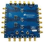
DS25BR100EVK Description
Figure 1 shows the top layer drawing of the PCB with the silkscreen annotations. It is a 4.5 by 4.5 inch
eight-layer PCB that has a three-device layout capable of demonstrating performance and all features of the
DS25BR100, DS25BR110 and DS25BR120. In addition, three microstrips allow easy evaluation of
transmit pre-emphasis and receive equalization.
Figure 1. Driver Board
Connector
CON1, CON2
CON3, CON4
CON5, CON6
Device
U1
U2
U3
Function
Select PE or EQ Level
Select EQ Level
Select PE Level
Table 1. Driver Board Connector-Device-Function Cross Reference
Page 4 of 8
�DS25BR100EVK User Manual
DS25BR100 (U1) Evaluation
The DS25BR100 is a 3.125 Gbps LVDS buffer featuring two levels of transmit pre-emphasis (Off and
Medium) and two levels of receive equalization (Low and Medium). The following is a recommended test
setup procedure for the device evaluation. Figure 2 depicts a typical setup and instrumentation used for the
device evaluation.
1.
Apply the power to the device (3.3V typical) between VDD and VSS banana plug receptacles.
2.
Connect desired STRIPLINE(s) to the input and / or output of the device using short 50-ohm
coaxial cables (e.g. PE-SR402-AL from www.pasternack.com).
3.
Connect a signal source (i.e. signal generator or an LVDS driver) to the IN1 inputs on the board
and adjust the signal parameters (VOH, VOL, VCM) so that they comply with the device input
recommendations.
4.
Select equalization level by setting the EQ pin (CON2) to L (for Low setting) or H (for Medium
setting).
5.
If a STRIPLINE is connected to the device outputs, select pre-emphasis level by setting the PE pin
(CON1) to L (for Off setting) or H (for Medium setting)
6.
Connect the OUT1 outputs to an oscilloscope and view the output signals with an oscilloscope
with the bandwidth of at least 5 GHz.
Figure 2. DS25BR100 Test Setup Example
Page 5 of 8
�DS25BR100EVK User Manual
DS25BR110 (U2) Evaluation
The DS25BR110 is a 3.125 Gbps LVDS buffer featuring four levels of receive equalization (Off, Low,
Medium and High). The following is a recommended test setup procedure for the device evaluation. Figure
3 depicts a typical setup and instrumentation used for the device evaluation.
1.
Apply the power to the device (3.3V typical) between VDD and VSS banana plug receptacles.
2.
Connect desired STRIPLINE to the input of the device using short 50-ohm coaxial cables (e.g.
PE-SR402-AL from www.pasternack.com).
3.
Connect a signal source (i.e. signal generator or an LVDS driver) to the IN2 inputs on the board
and adjust the signal parameters (VOH, VOL, VCM) so that they comply with the device input
recommendations.
4.
Select equalization level by setting the EQ0 (CON4) and EQ1 (CON3) pins to L or H. Refer to
Table 2.
EQ1
0
0
1
1
EQ0
0
1
0
1
Equalization Level
Off
Low
Medium
High
Table 2. Equalization Level Selection
5.
Connect the OUT2 outputs to an oscilloscope and view the output signals with an oscilloscope
with the bandwidth of at least 5 GHz.
Figure 3. DS25BR110 Test Setup Example
Page 6 of 8
�DS25BR100EVK User Manual
DS25BR120 (U3) Evaluation
The DS25BR120 is a 3.125 Gbps LVDS buffer featuring four levels of transmit pre-emphasis (Off, Low,
Medium and High). The following is a recommended test setup procedure for the device evaluation. Figure
4 depicts a typical setup and instrumentation used for the device evaluation.
1.
Apply the power to the device (3.3V typical) between VDD and VSS banana plug receptacles.
2.
Connect desired STRIPLINE to the output of the device using short 50-ohm coaxial cables (e.g.
PE-SR402-AL from www.pasternack.com).
3.
Connect a signal source (i.e. signal generator or an LVDS driver) to the IN3 inputs on the board
and adjust the signal parameters (VOH, VOL, VCM) so that they comply with the device input
recommendations.
4.
Select pre-emphasis level by setting the PE0 (CON5) and PE1 (CON6) pins to L or H. Refer to
Table 3.
PE1
0
0
1
1
PE0
0
1
0
1
Pre-emphasis Level
Off
Low
Medium
High
Table 3. Pre-emphasis Level Selection
5.
Connect the OUT3 outputs to an oscilloscope and view the output signals with an oscilloscope
with the bandwidth of at least 5 GHz.
Figure 4. DS25BR120 Test Setup Example
Page 7 of 8
�DS25BR100EVK User Manual
Typical Performance
This section of the User Manual shows typical eye diagrams you can expect to see when evaluating the
DS25BR100EVK.
The DS25BRxxx 3.125 Gbps PRBS-7 output eye
diagram without any STRIPLINE connected and with
PE/EQ = Off
The DS25BRxxx 3.125 Gbps PRBS-7 output eye
diagram after the STRIPLINE 3 and with PE/EQ =
Off
The DS25BR120 3.125 Gbps PRBS-7 output eye
diagram after the STRIPLINE 3 and with PE = High.
See Figure 4 for the Setup used.
The DS25BR110 3.125 Gbps PRBS-7 output eye
diagram after the STRIPLINE 3 and with EQ = High.
See Figure 3 for the Setup used.
Page 8 of 8
�ENERCON -
BILL OF MATERIALS
TITLE:
Main Product:
NATIONAL SEMICONDUCTOR
DS25BR100EVK ROHS
PCBA, DS20BR100-EVK,
Rev: Rev By: Rev Date:
PL Number:
Z3016-01 2
BJ
Responsible Eng/Mgr:
PCBA, DS25BR100EVK
DS20BR100-EVK, ROHS
Item Part Type
1 PCB
Part Number/Value
Mfg
P-05479R0
NoSub
Description
DS25BR100: 4.50x4.50x.062in, 8 layer
Qty
PL Status:
3/1/2007
Creation Date:
Arlene Fox
10/26/2006
Ref Des
SMT
1
Released
Creator:
Notes
Rev
Bd: (114.30x
114.30mm)
Panel: (
4.50x13.70in)
(114.30x
347.98mm) 3
bds/panel
0
2
3 IC
DS25BR100TSD
NAT
1
X
U1
Customer
Supplied
0
4 IC
DS25BR110TSD
NAT
1
X
U2
Customer
Supplied
0
5 IC
DS25BR120TSD
NAT
1
X
U3
Customer
Supplied
0
06035C103KAT
AVX
.01µF, 50V, ±10%, 0603, Ceramic, X7R,
Pb-Free
3
X
C2,6,8
0
C0603C103K5RAC
KEMET
.01µF, 50V, ±10%, 0603, Ceramic, X7R,
Pb-Free
ECJ-1VB1H103K
PANA
.01µF, 50V, ±10%, 0603, Ceramic, X7R,
Pb-Free
0603YC104KAT
AVX
.1µF, 16V, ±10%, 0603, Ceramic, X7R, PbFree
3
X
C3,5,7
0
C0603C104K3RAC
KEMET
.1µF, 25V, ±10%, 0603, Ceramic, X7R, PbFree
C0603C104K4RAC
KEMET
.1µF, 16V, ±10%, 0603, Ceramic, X7R, PbFree
ECJ-1VB1C104K
PANA
.1µF, 16V, ±10%, 0603, Ceramic, X7R, PbFree
ECJ-1VB1E104K
PANA
.1µF, 25V, ±10%, 0603, Ceramic, X7R, PbFree
TAJA106K016
AVX
10µF, 16V, ±10%, A-Case, Tantalum, PbFree
1
X
C1
0
T491A106K016AT
KEMET
10µF, 16V, ±10%, A-Case, Tantalum, PbFree
6
7
8 CAP
9 CAP
10 CAP
11
1:21:12 PM, 3/9/2007
Confidential and Proprietary. This document is considered uncontrolled unless stamped otherwise.
Page
1 of 2
�ENERCON -
BILL OF MATERIALS
TITLE:
Main Product:
NATIONAL SEMICONDUCTOR
DS25BR100EVK ROHS
PCBA, DS20BR100-EVK,
PL Number:
Rev: Rev By: Rev Date:
Z3016-01 2
BJ
Responsible Eng/Mgr:
PCBA, DS25BR100EVK
DS20BR100-EVK, ROHS
Item Part Type
Part Number/Value
Mfg
Description
NoSub
Qty
24
PL Status:
3/1/2007
Creation Date:
Arlene Fox
10/26/2006
Ref Des
SMT
Released
Creator:
Notes
Rev
12 CONN
142-0701-851
EMERSON
SMA, Jack Receptacle, 50 OHM, Pb-Free
SMA1-24
0
13 CONN
3267
POMONA
Banana, 1p, Female, Pb-Free
2
CON10,11
0
14 CONN
TSW-103-07-G-S
SAMTEC
Header, 3p, Male, .100"sp, Gold, Pb-Free
6
CON1-6
0
T-05481R0
ENERCON
STENCIL FABRICATION, DS25BR100-EVK, ROHS
1
18 REF
C-05480R0
ENERCON
FABRICATION DWG, DS25BR100-EVK, ROHS
0
19 REF
S-05475R0
ENERCON
SCHEMATIC,
DS25BR100-EVK, ROHS
0
20 REF
C-05491R0
ENERCON
PALLET DWG, DS25BR100-EVK, ROHS
0
15
16 STENCL
0
17
Notes:
Do Not Stuff Resistors R1, R2, and R3
1:21:12 PM, 3/9/2007
Confidential and Proprietary. This document is considered uncontrolled unless stamped otherwise.
Page
2 of 2
�DS25BR100EVK
�����IMPORTANT NOTICE
Texas Instruments Incorporated and its subsidiaries (TI) reserve the right to make corrections, modifications, enhancements, improvements,
and other changes to its products and services at any time and to discontinue any product or service without notice. Customers should
obtain the latest relevant information before placing orders and should verify that such information is current and complete. All products are
sold subject to TI’s terms and conditions of sale supplied at the time of order acknowledgment.
TI warrants performance of its hardware products to the specifications applicable at the time of sale in accordance with TI’s standard
warranty. Testing and other quality control techniques are used to the extent TI deems necessary to support this warranty. Except where
mandated by government requirements, testing of all parameters of each product is not necessarily performed.
TI assumes no liability for applications assistance or customer product design. Customers are responsible for their products and
applications using TI components. To minimize the risks associated with customer products and applications, customers should provide
adequate design and operating safeguards.
TI does not warrant or represent that any license, either express or implied, is granted under any TI patent right, copyright, mask work right,
or other TI intellectual property right relating to any combination, machine, or process in which TI products or services are used. Information
published by TI regarding third-party products or services does not constitute a license from TI to use such products or services or a
warranty or endorsement thereof. Use of such information may require a license from a third party under the patents or other intellectual
property of the third party, or a license from TI under the patents or other intellectual property of TI.
Reproduction of TI information in TI data books or data sheets is permissible only if reproduction is without alteration and is accompanied
by all associated warranties, conditions, limitations, and notices. Reproduction of this information with alteration is an unfair and deceptive
business practice. TI is not responsible or liable for such altered documentation. Information of third parties may be subject to additional
restrictions.
Resale of TI products or services with statements different from or beyond the parameters stated by TI for that product or service voids all
express and any implied warranties for the associated TI product or service and is an unfair and deceptive business practice. TI is not
responsible or liable for any such statements.
TI products are not authorized for use in safety-critical applications (such as life support) where a failure of the TI product would reasonably
be expected to cause severe personal injury or death, unless officers of the parties have executed an agreement specifically governing
such use. Buyers represent that they have all necessary expertise in the safety and regulatory ramifications of their applications, and
acknowledge and agree that they are solely responsible for all legal, regulatory and safety-related requirements concerning their products
and any use of TI products in such safety-critical applications, notwithstanding any applications-related information or support that may be
provided by TI. Further, Buyers must fully indemnify TI and its representatives against any damages arising out of the use of TI products in
such safety-critical applications.
TI products are neither designed nor intended for use in military/aerospace applications or environments unless the TI products are
specifically designated by TI as military-grade or "enhanced plastic." Only products designated by TI as military-grade meet military
specifications. Buyers acknowledge and agree that any such use of TI products which TI has not designated as military-grade is solely at
the Buyer's risk, and that they are solely responsible for compliance with all legal and regulatory requirements in connection with such use.
TI products are neither designed nor intended for use in automotive applications or environments unless the specific TI products are
designated by TI as compliant with ISO/TS 16949 requirements. Buyers acknowledge and agree that, if they use any non-designated
products in automotive applications, TI will not be responsible for any failure to meet such requirements.
Following are URLs where you can obtain information on other Texas Instruments products and application solutions:
Products
Applications
Audio
www.ti.com/audio
Automotive and Transportation www.ti.com/automotive
Amplifiers
amplifier.ti.com
Communications and Telecom www.ti.com/communications
Data Converters
dataconverter.ti.com
Computers and Peripherals
www.ti.com/computers
DLP® Products
www.dlp.com
Consumer Electronics
www.ti.com/consumer-apps
DSP
dsp.ti.com
Energy and Lighting
www.ti.com/energy
Clocks and Timers
www.ti.com/clocks
Industrial
www.ti.com/industrial
Interface
interface.ti.com
Medical
www.ti.com/medical
Logic
logic.ti.com
Security
www.ti.com/security
Power Mgmt
power.ti.com
Space, Avionics and Defense
www.ti.com/space-avionics-defense
Microcontrollers
microcontroller.ti.com
Video and Imaging
www.ti.com/video
RFID
www.ti-rfid.com
OMAP Mobile Processors
www.ti.com/omap
Wireless Connectivity
www.ti.com/wirelessconnectivity
TI E2E Community Home Page
e2e.ti.com
Mailing Address: Texas Instruments, Post Office Box 655303, Dallas, Texas 75265
Copyright © 2012, Texas Instruments Incorporated
�


 工商网监
湘ICP备2023018690号
工商网监
湘ICP备2023018690号
