DS3658
www.ti.com
SNLS365B – MARCH 1995 – REVISED APRIL 2013
DS3658 Quad High Current Peripheral Driver
Check for Samples: DS3658
FEATURES
DESCRIPTION
•
•
•
•
The DS3658 quad peripheral driver is designed for
those applications where low operating power, high
breakdown voltage, high output current and low
output ON voltage are required. A unique input circuit
combines TTL compatibility with high impedance. In
fact, its extreme low input current allows it to be
driven directly by a CMOS device.
1
2
•
•
•
•
•
•
•
•
•
•
•
•
•
Single Saturated Transistor Outputs
Low Standby Power, 10 mW Typical
High Impedance TTL Compatible Inputs
Outputs May Be Tied Together for Increased
Current Capacity
High Output Current
– 600 mA Per Output
– 2.4A Per Package
No Output Latch-up at 35V
Low Output ON Voltage (350 mV typ @ 600
mA)
High Breakdown Voltage (70V)
Open Collector Outputs
Output Clamp Diodes for Inductive Fly Back
Protection
NPN Inputs for Minimal Input Currents (1 µA
Typical)
Low Operating Power
Standard 5V Power Supply
Power Up/Down Protection
Fail Safe Operation
2W Power Package
Pin-for-Pin Compatible with SN75437
The outputs are capable of sinking 600 mA each and
offer a 70V breakdown. However, for inductive loads
the output should be clamped to 35V or less to avoid
latch-up during turn off (inductive fly back
protection—refer to AN-213 'SNOA610'). An on-chip
clamp diode capable of handling 800 mA is provided
at each output for this purpose. In addition, the
DS3658 incorporates circuitry that specifies glitchfree power up or down operation and a fail-safe
feature which puts the output in a high impedance
state when the input is open.
The PDIP package is specifically constructed to allow
increased power dissipation over conventional
packages. The four ground pins are directly
connected to the device chip with a special cooper
lead frame. When the quad driver is soldered into a
PC board, the power rating of the device improves
significantly.
APPLICATIONS
•
•
•
•
•
•
•
•
•
•
Relay Drivers
Lamp Drivers
Solenoid Drivers
Hammer Drivers
Stepping Motor Drivers
Triac Drivers
LED Drivers
High Current, High Voltage Drivers
Level Translators
Fiber Optic LED Drivers
1
2
Please be aware that an important notice concerning availability, standard warranty, and use in critical applications of
Texas Instruments semiconductor products and disclaimers thereto appears at the end of this data sheet.
All trademarks are the property of their respective owners.
PRODUCTION DATA information is current as of publication date.
Products conform to specifications per the terms of the Texas
Instruments standard warranty. Production processing does not
necessarily include testing of all parameters.
Copyright © 1995–2013, Texas Instruments Incorporated
�DS3658
SNLS365B – MARCH 1995 – REVISED APRIL 2013
www.ti.com
Connection Diagram
Figure 1. PDIP- Top View
See Package Number NFG0016E
These devices have limited built-in ESD protection. The leads should be shorted together or the device placed in conductive foam
during storage or handling to prevent electrostatic damage to the MOS gates.
Absolute Maximum Ratings
(1) (2)
Supply Voltage
7V
Input Voltage
15V
Output Voltage
70V
Output Current
Continuous Power Dissipation @ 25°C Free-Air
1.5A
(3)
2075 mW
−65°C to +150°C
Storage Temperature Range
Lead Temperature (Soldering, 4 sec.)
(1)
(2)
(3)
260°C
“Absolute Maximum Ratings” are those values beyond which the safety of the device cannot be specified. They are not meant to imply
that the device should be operated at these limits. Electrical Characteristics provides conditions for actual device operation.
If Military/Aerospace specified devices are required, please contact the Texas Instruments Sales Office/ Distributors for availability and
specifications.
For operation over 25° free-air temperature, derate linearly to 1328 mW @ 70°C @ the rate of 16.6 mW/°C.
Operating Conditions
Supply Voltage
Ambient Temperature
2
Min
Max
4.75
5.25
V
0
70
°C
Submit Documentation Feedback
Units
Copyright © 1995–2013, Texas Instruments Incorporated
Product Folder Links: DS3658
�DS3658
www.ti.com
SNLS365B – MARCH 1995 – REVISED APRIL 2013
Electrical Characteristics (1) (2)
Symbol
Parameter
Conditions
VIH
Input High Voltage
VIL
Input Low Voltage
IIH
Input High Current
VIN = 5.25V, VCC = 5.25V
IIL
Input Low Current
VIN = 0.4V
VIK
Input Clamp Voltage
VOL
Output Low Voltage
Min
Typ
Max
Units
2.0
V
0.8
V
1.0
1.0
µA
±10
µA
II = −12 mA
−0.8
−1.5
V
IL = 300 mA
0.2
0.4
V
IL = 600 mA
(3)
0.35
0.7
V
100
µA
1.6
V
ICEX
Output Leakage Current
VCE = 70V, VIN = 0.8V
VF
Diode Forward Voltage
IF = 800 mA
IR
Diode Leakage Current
VR = 70V
100
µA
ICC
Supply Current
All Inputs High
60
85
mA
All Inputs Low
2
4
mA
(1)
1.0
Unless otherwise specified, min/max limits apply across the 0°C to +70°C temperature range and the 4.75V to 5.25V power supply
range. All typical values are for TA = 25°C and VCC = 5.0V.
All currents into device pins are shown as positive, all currents out of device pins are shown as negative, all voltages are referenced to
ground, unless otherwise specified. All values shown as max or min are so classified on absolute value basis.
All sections of this quad circuit may conduct rated current simultaneously, however, power dissipation averaged over a short interval of
time must fall within specified continuous dissipation ratings.
(2)
(3)
Switching Characteristics (1)
Typ
Max
Units
tPHL
Symbol
Turn On Delay
RL = 60Ω, VL = 30V
226
500
ns
tPLH
Turn Off Delay
RL = 60Ω, VL = 30V
2430
8000
ns
(1)
Parameter
Conditions
Min
Unless otherwise specified, min/max limits apply across the 0°C to +70°C temperature range and the 4.75V to 5.25V power supply
range. All typical values are for TA = 25°C and VCC = 5.0V.
Truth Table (1)
(1)
IN
EN
OUT
H
H
L
L
H
Z
H
L
Z
L
L
Z
H = High state
L = Low state
Z = High impedance state
Submit Documentation Feedback
Copyright © 1995–2013, Texas Instruments Incorporated
Product Folder Links: DS3658
3
�DS3658
SNLS365B – MARCH 1995 – REVISED APRIL 2013
www.ti.com
AC Test Circuit
Figure 2.
Switching Waveforms
Figure 3.
Typical Applications
Figure 4. Stepping Motor Driver
4
Submit Documentation Feedback
Figure 5. Lamp Driver
Copyright © 1995–2013, Texas Instruments Incorporated
Product Folder Links: DS3658
�DS3658
www.ti.com
SNLS365B – MARCH 1995 – REVISED APRIL 2013
REVISION HISTORY
Changes from Revision A (April 2013) to Revision B
•
Page
Changed layout of National Data Sheet to TI format ............................................................................................................ 4
Submit Documentation Feedback
Copyright © 1995–2013, Texas Instruments Incorporated
Product Folder Links: DS3658
5
�PACKAGE OPTION ADDENDUM
www.ti.com
16-Nov-2017
PACKAGING INFORMATION
Orderable Device
Status
(1)
Package Type Package Pins Package
Drawing
Qty
Eco Plan
Lead/Ball Finish
MSL Peak Temp
(2)
(6)
(3)
Op Temp (°C)
Device Marking
(4/5)
DS3658N
LIFEBUY
PDIP
NFG
16
25
TBD
Call TI
Call TI
0 to 70
DS3658N
DS3658N/NOPB
LIFEBUY
PDIP
NFG
16
25
Green (RoHS
& no Sb/Br)
CU SN
Level-1-NA-UNLIM
0 to 70
DS3658N
(1)
The marketing status values are defined as follows:
ACTIVE: Product device recommended for new designs.
LIFEBUY: TI has announced that the device will be discontinued, and a lifetime-buy period is in effect.
NRND: Not recommended for new designs. Device is in production to support existing customers, but TI does not recommend using this part in a new design.
PREVIEW: Device has been announced but is not in production. Samples may or may not be available.
OBSOLETE: TI has discontinued the production of the device.
(2)
RoHS: TI defines "RoHS" to mean semiconductor products that are compliant with the current EU RoHS requirements for all 10 RoHS substances, including the requirement that RoHS substance
do not exceed 0.1% by weight in homogeneous materials. Where designed to be soldered at high temperatures, "RoHS" products are suitable for use in specified lead-free processes. TI may
reference these types of products as "Pb-Free".
RoHS Exempt: TI defines "RoHS Exempt" to mean products that contain lead but are compliant with EU RoHS pursuant to a specific EU RoHS exemption.
Green: TI defines "Green" to mean the content of Chlorine (Cl) and Bromine (Br) based flame retardants meet JS709B low halogen requirements of
很抱歉,暂时无法提供与“DS3658N/NOPB”相匹配的价格&库存,您可以联系我们找货
免费人工找货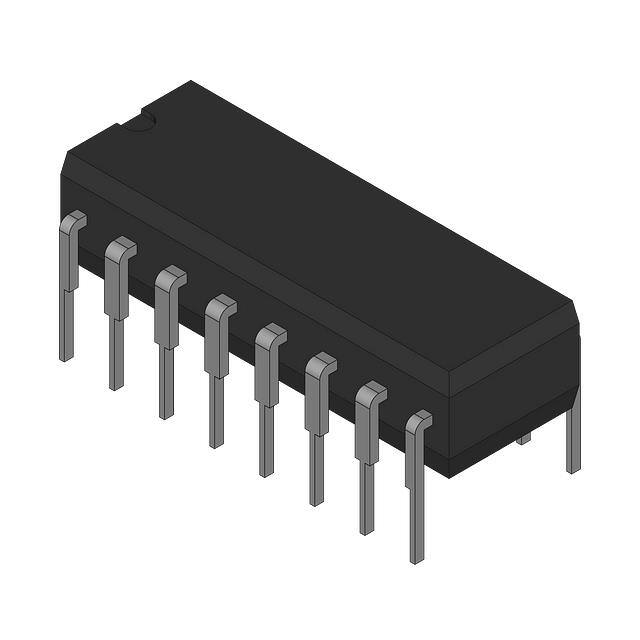


 工商网监
湘ICP备2023018690号
工商网监
湘ICP备2023018690号
