Sample &
Buy
Product
Folder
Support &
Community
Tools &
Software
Technical
Documents
DS90UB927Q-Q1
SNLS416D – JUNE 2012 – REVISED JANUARY 2015
DS90UB927Q-Q1 5-MHz to 85-MHz 24-bit Color FPD-Link III Serializer
With Bidirectional Control Channel
1 Features
•
1
•
•
•
•
•
•
•
•
•
•
•
•
•
•
•
3 Description
The DS90UB927Q-Q1 serializer, in conjunction with a
DS90UB928Q-Q1 or DS90UB926Q-Q1 deserializer,
provides a complete digital interface for concurrent
transmission of high-speed video, audio, and control
data for automotive display and image sensing
applications.
2
Bidirectional Control Channel Interface with I Ccompatible Serial Control Bus
Low EMI FPD-Link Video Input
Supports High Definition (720p) Digital Video
Format
5-MHz to 85-MHz PCLK Supported
RGB888 + VS, HS, DE and I2S Audio Supported
Up to 4 I2S Digital Audio Inputs for Surround
Sound Applications
4 Bidirectional GPIO Channels with 2 Dedicated
Pins
Single 3.3-V Supply with 1.8-V or 3.3-V
Compatible LVCMOS I/O Interface
AC-Coupled STP Interconnect Up to 10 Meters
DC-Balanced and Scrambled Data With
Embedded Clock
Supports Repeater Application
Internal Pattern Generation
Low Power Modes Minimize Power Dissipation
Automotive Grade Product: AEC-Q100 Grade 2
Qualified
>8-kV HBM and ISO 10605 ESD Rating
Backward Compatible Modes
The chipset is ideally suited for automotive video
display systens with HD formats and automotive
vision systems with megapixel resolutions. The
DS90UB927Q-Q1
incorporates
an
embedded
bidirectional control channel and low latency GPIO
controls. This device translates a FPD-Link video
interface into a single-pair high-speed serialized
interface. The FPD-Link III serial bus scheme
supports full duplex, high speed forward channel data
transmission
and
low-speed
back
channel
communication over a single differential link.
Consolidation of audio, video, and control data over a
single differential pair reduces the interconnect size
and weight, while also eliminating skew issues and
simplifying system design.
The DS90UB927Q-Q1 serializer embeds the clock
and level shifts the signals to high-speed differential
signaling. Up to 24 RGB data bits are serialized along
with three video control signals, and up to four I2S
data inputs.
The FPD-Link data interface allows for easy
interfacing with data sources while also minimizing
EMI and bus width. EMI on the high-speed FPD-Link
III bus is minimized using low voltage differential
signaling, data scrambling and randomization, and
DC-balancing.
2 Applications
•
•
•
•
Automotive Displays for Navigation
Rear Seat Entertainment Systems
Automotive Driver Assistance
Automotive Megapixel Camera Systems
Device Information(1)
PART NUMBER
DS90UB927Q-Q1
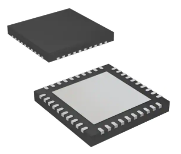
PACKAGE
WQFN (40)
BODY SIZE (NOM)
6.00 mm x 6.00 mm
(1) For all available packages, see the orderable addendum at
the end of the datasheet.
Application Diagram
FPD-Link
FPD-Link
VDDIO
VDD33
(3.3V) (1.8V or 3.3V)
HOST
Graphics
Processor
FPD-Link Display Interface
VDD33
VDDIO
(1.8V or 3.3V) (3.3V)
RxIN3+/-
RxIN1+/RxIN0+/RxCLKIN+/-
TxOUT2+/-
DOUT+
RIN+
DOUT-
RIN100Q STP Cable
DS90UB927Q-Q1
Serializer
PDB
INTB
I2S 6
SCL
SDA
IDx
TxOUT3+/-
FPD-Link III
1 Pair/AC Coupled
RxIN2+/-
MAPSEL
LFMODE
REPEAT
BKWD
OEN
OSS_SEL
PDB
MAPSEL
LFMODE
BISTEN
MODE_SEL
DS90UB928Q-Q1
Deserializer
TxOUT1+/TxOUT0+/-
RGB Display
720p
24-bit Color Depth
TxCLKOUT+/INTB_IN
LOCK
PASS
6
I2S
MCLK
SCL
SDA
IDx
1
An IMPORTANT NOTICE at the end of this data sheet addresses availability, warranty, changes, use in safety-critical applications,
intellectual property matters and other important disclaimers. PRODUCTION DATA.
�DS90UB927Q-Q1
SNLS416D – JUNE 2012 – REVISED JANUARY 2015
www.ti.com
Table of Contents
1
2
3
4
5
6
Features ..................................................................
Applications ...........................................................
Description .............................................................
Revision History.....................................................
Pin Configuration and Functions .........................
Specifications.........................................................
1
1
1
2
3
5
6.1
6.2
6.3
6.4
6.5
6.6
6.7
Absolute Maximum Ratings ...................................... 5
ESD Ratings.............................................................. 5
Recommended Operating Conditions....................... 6
Thermal Information .................................................. 6
DC Electrical Characteristics .................................... 7
AC Electrical Characteristics..................................... 9
Electrical Characteristics: DC and AC Serial Control
Bus ........................................................................... 10
6.8 Timing Requirements for the Serial Control Bus .... 11
6.9 Timing Requirements - DC and AC Serial Control
Bus Characteristics .................................................. 11
6.10 Typical Characteristics .......................................... 14
7
Detailed Description ............................................ 15
7.1 Overview ................................................................. 15
7.2
7.3
7.4
7.5
7.6
8
Functional Block Diagram .......................................
Feature Description.................................................
Device Functional Modes........................................
Programming...........................................................
Register Maps .........................................................
15
16
23
29
31
Application and Implementation ........................ 44
8.1 Application Information............................................ 44
8.2 Typical Application .................................................. 44
8.3 System Examples ................................................... 46
9 Power Supply Recommendations...................... 48
10 Layout................................................................... 48
10.1 Layout Guidelines ................................................. 48
10.2 Layout Example .................................................... 49
11 Device and Documentation Support ................. 51
11.1
11.2
11.3
11.4
Documentation Support ........................................
Trademarks ...........................................................
Electrostatic Discharge Caution ............................
Glossary ................................................................
51
51
51
51
12 Mechanical, Packaging, and Orderable
Information ........................................................... 51
4 Revision History
NOTE: Page numbers for previous revisions may differ from page numbers in the current version.
Changes from Revision C (October 2012) to Revision D
•
Added ESD Ratings table, Feature Description section, Device Functional Modes, Application and Implementation
section, Power Supply Recommendations section, Layout section, Device and Documentation Support section, and
Mechanical, Packaging, and Orderable Information section .................................................................................................. 1
Changes from Revision B (June 2012) to Revision C
•
2
Page
Page
Changed layout of National data sheet to tI format.............................................................................................................. 49
Submit Documentation Feedback
Copyright © 2012–2015, Texas Instruments Incorporated
Product Folder Links: DS90UB927Q-Q1
�DS90UB927Q-Q1
www.ti.com
SNLS416D – JUNE 2012 – REVISED JANUARY 2015
5 Pin Configuration and Functions
RxIN1-
RxIN0-
CAPLVD12
INTB
VDD33_B
LFMODE
VDDIO
MAPSEL
BKWD
REPEAT
29
28
27
26
25
24
23
22
21
30
RxIN0+
RTA Package
40-Pin WQFN With Exposed Thermal Pad
Top View
31
DAP = GND
20
CMF
19
VDD33_A
RxIN1+
32
RxIN2-
33
18
PDB
RxIN2+
34
17
DOUT+
RxCLKIN-
35
16
DOUT-
RxCLKIN+
36
15
RES1
RxIN3-
37
14
CAPHS12
RxIN3+
38
13
RES0
GPIO0
39
12
CAPP12
GPIO1
40
11
IDx
5
6
7
8
9
10
I2S_DC/GPI02
I2S_DD/GPI03
VDDIO
CAPL12
SCL
SDA
3
I2S_DA/GPIO_REG6
4
2
I2S_CLK/GPIO_REG8
I2S_DB/GPIO_REG5
1
I2S_WC/GPIO_REG7
DS90UB927Q-Q1
Pin Functions
PIN
NAME
I/O
NO.
DESCRIPTION
FPD-LINK INPUT INTERFACE
RxCLKIN-
35
I, LVDS
Inverting LVDS Clock Input
The pair requires external 100-Ω differential termination for standard LVDS levels
RxCLKIN+
36
I, LVDS
True LVDS Clock Input
The pair requires external 100-Ω differential termination for standard LVDS levels
RxIN[3:0]-
37, 33,
31, 29
I, LVDS
Inverting LVDS Data Inputs
Each pair requires external 100-Ω differential termination for standard LVDS levels
RxIN[3:0]+
38, 34,
32, 30
I, LVDS
True LVDS Data Inputs
Each pair requires external 100-Ω differential termination for standard LVDS levels
LVCMOS PARALLEL INTERFACE
BKWD
GPIO[1:0]
22
40, 39
Backward Compatible Mode Select
I, LVCMOS BKWD = 0, interfacing to DS90UH926/8Q-Q1 (Default)
with pulldown BKWD = 1, interfacing to DS90UR906/8Q-Q1, DS90UR916Q
Requires a 10-kΩ pullup if set HIGH
I/O, LVCMOS General Purpose I/O
with pulldown See Table 1
I2S_DA
I2S_DB
I2S_DC
I2S_DD
3
4
5
6
I, LVCMOS Digital Audio Interface I2S Data Inputs
with pulldown Shared with GPIO_REG6, GPIO_REG5, GPIO2, GPIO3
I2S_WC
I2S_CLK
1
2
I, LVCMOS Digital Audio Interface I2S Word Clock and I2S Bit Clock Inputs
with pulldown Shared with GPIO_REG7 and GPIO_REG8 (Table 3)
Submit Documentation Feedback
Copyright © 2012–2015, Texas Instruments Incorporated
Product Folder Links: DS90UB927Q-Q1
3
�DS90UB927Q-Q1
SNLS416D – JUNE 2012 – REVISED JANUARY 2015
www.ti.com
Pin Functions (continued)
PIN
NAME
I/O
NO.
DESCRIPTION
25
Low Frequency Mode Select
I, LVCMOS LFMODE = 0, 15 MHz ≤ RxCLKIN ≤ 85 MHz (Default)
with pulldown LFMODE = 1, 5 MHz ≤ RxCLKIN < 15 MHz
Requires a 10-kΩ pullup if set HIGH
MAPSEL
23
FPD-Link Input Map Select
MAPSEL = 0, LSBs on RxIN3± (Default)
I, LVCMOS
MAPSEL = 1, MSBs on RxIN3±
with pulldown
See Figure 19 and Figure 20
Requires a 10-kΩ pullup if set HIGH
REPEAT
21
Repeater Mode Select
I, LVCMOS REPEAT = 0, Repeater Mode disabled (Default)
with pulldown REPEAT = 1, Repeater Mode enabled
Requires a 10-kΩ pullup if set HIGH
LFMODE
OPTIONAL PARALLEL INTERFACE
GPIO[3:2]
GPIO_REG
[8:5]
6, 5
2, 1, 3, 4
I/O, LVCMOS General Purpose I/O
with pulldown Shared with I2S_DD and I2S_DC (See Table 1)
I/O, LVCMOS Register-Only General Purpose I/O
with pulldown Shared with I2S_CLK, I2S_WC, I2S_DA, I2S_DB (See Table 2)
CONTROL AND CONFIGURATION
IDx
11
I, Analog
I2C Address Select
External pullup to VDD33 is required under all conditions. DO NOT FLOAT.
Connect to external pullup to VDD33 and pulldown to GND to create a voltage divider.
See Figure 25 and Table 4
PDB
18
Power-down Mode Input Pin
Must be driven or pulled up to VDD33. Refer to Power Supply Recommendations.
I, LVCMOS PDB = H, device is enabled (normal operation)
with pulldown PDB = L, device is powered down.
When the device is in the powered down state, the Driver Outputs are both HIGH, the PLL is
shutdown, and IDD is minimized. Control Registers are RESET.
SCL
9
I2C Clock Input / Output Interface
I/O, LVCMOS
Must have an external pullup to VDD33. DO NOT FLOAT.
Open Drain
Recommended pullup: 4.7 kΩ.
10
I2C Data Input / Output Interface
I/O, LVCMOS
Must have an external pullup to VDD33. DO NOT FLOAT.
Open Drain
Recommended pullup: 4.7 kΩ.
27
O, LVCMOS
Open Drain
SDA
STATUS
INTB
Interrupt
INTB = H, normal
INTB = L, Interrupt request
Recommended pullup: 4.7 kΩ to VDDIO. DO NOT FLOAT.
FPD-LINK III SERIAL INTERFACE
Common Mode Filter.
Connect 0.1 µF to GND (required)
CMF
20
Analog
DOUT-
16
I/O, LVDS
Inverting Output
The output must be AC-coupled with a 0.1-µF capacitor.
DOUT+
17
I/O, LVDS
True Output
The output must be AC-coupled with a 0.1-µF capacitor.
4
Submit Documentation Feedback
Copyright © 2012–2015, Texas Instruments Incorporated
Product Folder Links: DS90UB927Q-Q1
�DS90UB927Q-Q1
www.ti.com
SNLS416D – JUNE 2012 – REVISED JANUARY 2015
Pin Functions (continued)
PIN
NAME
NO.
I/O
DESCRIPTION
POWER (1) AND GROUND
GND
VDD33_A
VDD33_B
VDDIO
DAP
Ground
Large metal contact at the bottom center of the device package Connect to the ground
plane (GND) with at least 9 vias.
19
26
Power
Power to on-chip regulator 3.0 V - 3.6 V. Each pin requires a 4.7-µF capacitor to GND
7, 24
Power
LVCMOS I/O Power 1.8 V ±5% OR 3.0 V - 3.6 V. Each pin requires 4.7-µF capacitor to GND
REGULATOR CAPACITOR
CAPL12
8
CAP
Decoupling capacitor connection for on-chip regulator
Requires two 4.7-µF decoupling capacitors to GND
CAPP12
CAPHS12
CAPLVD12
12
14
28
CAP
Decoupling capacitor connection for on-chip regulator
Each requires a 4.7-µF decoupling capacitor to GND.
15, 13
GND
Reserved
Connect to GND.
OTHER
RES[1:0]
(1)
The VDD (VDD33 and VDDIO) supply ramp should be faster than 1.5 ms with a monotonic rise.
6 Specifications
6.1 Absolute Maximum Ratings (1) (2) (3)
MIN
MAX
UNIT
Supply Voltage – VDD33
−0.3
4.0
V
Supply Voltage – VDDIO
−0.3
4.0
V
LVCMOS I/O Voltage
−0.3
VDDIO + 0.3
V
Serializer Output Voltage
−0.3
2.75
V
150
°C
150
°C
Junction Temperature
−65
Storage Temperature, Tstg
(1)
(2)
(3)
For soldering specifications: see product folder at www.ti.com and SNOA549.
Stresses beyond those listed under Absolute Maximum Ratings may cause permanent damage to the device. These are stress ratings
only, which do not imply functional operation of the device at these or any other conditions beyond those indicated under Recommended
Operating Conditions. Exposure to absolute-maximum-rated conditions for extended periods may affect device reliability.
If Military/Aerospace specified devices are required, please contact the Texas Instruments Sales Office/Distributors for availability and
specifications.
6.2 ESD Ratings
VALUE
V(ESD)
Electrostatic
discharge
Human body model (HBM), per AEC Q100-002 (1)
±8000
Charged device model (CDM), per AEC Q100-011
±1250
Machine model (MM)
±250
(IEC 61000-4-2, powered-up only)
RD = 330 Ω, CS = 150 pF
(ISO 10605)
RD = 330 Ω, CS = 150 pF/330 pF
RD = 2 kΩ, CS = 150 pF/330 pF
(1)
Air Discharge
(Pin 16 and 17)
±15000
Contact Discharge
(Pin 16 and 17)
±8000
Air Discharge
(Pin 16 and 17)
±15000
Contact Discharge
(Pin 16 and 17)
±8000
UNIT
V
AEC Q100-002 indicates HBM stressing is done in accordance with the ANSI/ESDA/JEDEC JS-001 specification.
Submit Documentation Feedback
Copyright © 2012–2015, Texas Instruments Incorporated
Product Folder Links: DS90UB927Q-Q1
5
�DS90UB927Q-Q1
SNLS416D – JUNE 2012 – REVISED JANUARY 2015
www.ti.com
6.3 Recommended Operating Conditions
over operating free-air temperature range (unless otherwise noted)
Supply Voltage (VDD33)
LVCMOS Supply Voltage (VDDIO) (1)
MIN
NOM
MAX
3.0
3.3
3.6
Connect VDDIO to 3.3 V and use 3.3-V IOs
3.0
3.3
3.6
Connect VDDIO to 1.8 V and use 1.8-V IOs
1.71
1.8
1.89
−40
+25
+105
Operating Free Air Temperature (TA)
PCLK Frequency
5
Supply Noise (2)
(1)
(2)
UNIT
V
V
°C
85
MHz
100
mVP-P
VDDIO < VDD33 + 0.3 V
Supply noise testing was done with minimum capacitors on the PCB. A sinusoidal signal is AC coupled to the VDD33 and VDDIO supplies
with amplitude = 100 mVp-p measured at the device VDD33 and VDDIO pins. Bit error rate testing of input to the Ser and output of the
Des with 10 meter cable shows no error when the noise frequency on the Ser is less than 50 MHz. The Des on the other hand shows no
error when the noise frequency is less than 50 MHz.
6.4 Thermal Information
DS90UB927Q-Q1
THERMAL METRIC (1)
RTA (WQFN)
UNIT
40 PINS
RθJA
Junction-to-ambient thermal resistance
29.0
RθJC(top)
Junction-to-case (top) thermal resistance
14.4
RθJB
Junction-to-board thermal resistance
5.1
ψJT
Junction-to-top characterization parameter
0.2
ψJB
Junction-to-board characterization parameter
5.1
RθJC(bot)
Junction-to-case (bottom) thermal resistance
1.4
(1)
6
°C/W
For more information about traditional and new thermal metrics, see the IC Package Thermal Metrics application report, SPRA953.
Submit Documentation Feedback
Copyright © 2012–2015, Texas Instruments Incorporated
Product Folder Links: DS90UB927Q-Q1
�DS90UB927Q-Q1
www.ti.com
SNLS416D – JUNE 2012 – REVISED JANUARY 2015
6.5 DC Electrical Characteristics
Over recommended operating supply and temperature ranges unless otherwise specified. (1) (2) (3)
PARAMETER
TEST CONDITIONS
PIN / FREQ
MIN
NOM
MAX
UNIT
2.0
VDDIO
V
GND
0.8
V
LVCMOS I/O
VIH
High Level Input
Voltage
VDDIO = 3.0 V to 3.6 V (4)
VIL
Low Level Input
Voltage
VDDIO = 3.0 V to 3.6 V (4)
IIN
Input Current
VIN = 0 V or VDDIO = 3.0 V to 3.6 V (4)
−15
+15
μA
High Level Input
Voltage
VDDIO = 3.0 V to 3.6 V
2.0
VDDIO
V
0.65*VDDIO
VDDIO
V
GND
0.8
V
GND
0.35*
VDDIO
V
VIH
VDDIO = 1.71 V to 1.89 V
VDDIO = 3.0 V to 3.6 V
VIL
Low Level Input
Voltage
IIN
Input Current
VOH
High Level Output
IOH = −4 mA
Voltage
VOL
Low Level Output
Voltage
IOS
Output Short
Circuit Current
VOUT = 0 V
IOZ
Tri-state Output
Current
VOUT = 0 V or VDDIO, PDB = L
(1)
(2)
(3)
(4)
VDDIO = 1.71 V to 1.89 V
VDDIO = 3.0 V to 3.6 V
VIN = 0 V or VDDIO VDDIO = 1.71 V to 1.89
V
IOL = +4 mA
PDB
GPIO[1:0]
I2S_CLK
I2S_WC
I2S_D[A,B,C,D]
LFMODE
MAPSEL
BKWD
REPEAT
±1
−15
±1
+15
μA
−15
±1
+15
μA
VDDIO = 3.0 V to 3.6 V
2.4
VDDIO
V
VDDIO = 1.71 V to 1.89
V
VDDIO 0.45
VDDIO
V
GND
0.4
V
GND
0.45
V
VDDIO = 3.0 V to 3.6 V
VDDIO = 1.71 V to 1.89
V
GPIO[3:0],
GPO_REG[8:5]
−55
−15
mA
+15
μA
The Electrical Characteristics tables list verified specifications under the listed Recommended Operating Conditions except as otherwise
modified or specified by the Electrical Characteristics conditions and/or notes. Typical specifications are estimations only and are not
verified.
Typical values represent most likely parametric norms at VDD33 = 3.3 V, VDDIO = 1.8 V or 3.3 V, TA = 25°C, and at the Recommended
Operating Conditions at the time of product characterization and are not verified.
Current into device pins is defined as positive. Current out of a device pin is defined as negative. Voltages are referenced to ground
except VOD and ΔVOD, which are differential voltages. Supply noise testing was done with minimum capacitors on the PCB. A sinusoidal
signal is AC coupled to the supply pins with amplitude = 100 mVp-p measured at the device VDD33 and VDDIO pins. Bit error rate testing
of input to the serializer and output of the deserializer with 10 meter cable shows no error when the noise frequency is less than 50
MHz.
PDB is specified to 3.3 V LVCMOS only and must be driven or pulled up to VDD33 or to VDDIO ≥ 3.0 V
Submit Documentation Feedback
Copyright © 2012–2015, Texas Instruments Incorporated
Product Folder Links: DS90UB927Q-Q1
7
�DS90UB927Q-Q1
SNLS416D – JUNE 2012 – REVISED JANUARY 2015
www.ti.com
DC Electrical Characteristics (continued)
Over recommended operating supply and temperature ranges unless otherwise specified.(1)(2)(3)
PARAMETER
TEST CONDITIONS
PIN / FREQ
MIN
NOM
MAX
UNIT
+100
mV
FPD-LINK LVDS RECEIVER
VTH
Threshold High
Voltage
VTL
Threshold Low
Voltage
|VID|
Differential Input
Voltage Swing
VCM
Common Mode
Voltage
IIN
Input Current
mV
−100
VCM = 1.2 V
RxCLKIN±
RxIN[3:0]±
200
0
600
mV
2.4
V
+10
μA
1000
1200
mVp-p
1
50
1.2
−10
FPD-LINK III CML DRIVER
Differential Output
VODp-p Voltage (DOUT+) RL = 100 Ω (Figure 1)
– (DOUT-)
ΔVOD
Output Voltage
Unbalance
VOS
Offset Voltage –
Single-ended
800
2.5-0.25*
VODp-p
RL = 100 Ω (Figure 1)
mV
V
(TYP)
ΔVOS
Offset Voltage
Unbalance
Single-ended
IOS
Output Short
Circuit Current
RT
Internal
Termination
Resistance Differential
DOUT±
1
DOUT+/- = 0 V, PDB = L or H (5)
50
−30
mV
mA
100
120
Ω
VDD33= 3.6 V
135
160
mA
VDDIO = 3.6 V
100
500
μA
VDDIO = 1.89 V
200
600
VDD33= 3.6 V
133
mA
VDDIO = 3.6 V
100
μA
VDDIO = 1.89 V
100
VDD33 = 3.6 V
1.2
2.4
mA
VDDIO = 3.6 V
4
30
μA
VDDIO = 1.89 V
5
30
μA
VDD33 = 3.6 V
1
2.2
mA
VDDIO = 3.6 V
8
20
μA
VDDIO = 1.89 V
4
20
μA
80
SUPPLY CURRENT
IDD1
IDDIO1
IDD2
Checkerboard Pattern (Figure 8)
Supply Current
RL = 100 Ω,
PCLK = 85 MHz
IDDIO2
IDDS
IDDIOS
Supply Current –
Remote Auto
Power Down
Random Pattern
PRBS7
reg_0x01[7]=1, Back channel Idle
IDDZ
IDDIOZ
(5)
8
Supply Current –
Power Down
PDB = 0 V, All other LVCMOS inputs = 0 V
μA
μA
IOS is not specified for an indefinite period of time. Do not hold in short circuit for more than 500 ms or part damage may result
Submit Documentation Feedback
Copyright © 2012–2015, Texas Instruments Incorporated
Product Folder Links: DS90UB927Q-Q1
�DS90UB927Q-Q1
www.ti.com
SNLS416D – JUNE 2012 – REVISED JANUARY 2015
6.6 AC Electrical Characteristics
over operating free-air temperature range (unless otherwise noted) (1) (2) (3)
PARAMETER
TEST CONDITIONS
PIN / FREQ
MIN
TYP
MAX
UNIT
RxCLKIN±,
RXIN[3:0]±
0.25
0.5
0.75
UI
100
140
ps
100
140
ps
5
ms
FPD-LINK LVDS INPUT
tRSP
Receiver Strobe Position
See Figure 4
AC ELECTRICAL CHARACTERISTICS - FPD-LINK III CML IO
tLHT
CML Output Low-to-High
Transition Time
See Figure 3
tHLT
CML Output High-to-Low
Transition Time
tPLD
Serializer PLL
Lock Time
See Figure 5 (4)
tSD
Delay — Latency
See Figure 6
tTJIT
Output Total Jitter,
Bit Error Rate ≤1E-9
Figure 7 (5) (6) (7) (8) (9)
tIJIT
Input Jitter Tolerance, Bit
Error Rate ≤1E-9 (6) (10)
Checkerboard Pattern
PCLK=5 MHz, Figure 8
Checkerboard Pattern
PCLK=85 MHz, Figure 8
f/40 < Jitter Freq < f/20,
DES = DS90UB926Q-Q1
f/40 < Jitter Freq < f/20,
DES = DS90UB928Q-Q1
DOUT+, DOUT-
PCLK = 5MHz
to 85MHz
146*T
ns
0.17
0.2
UI
0.26
0.29
UI
RxCLKIN±
RxCLKIN±,
f = 78 MHz
0.6
UI
0.5
UI
>4/PCLK
or >77
ns
AC ELECTRICAL CHARACTERISTICS - I2S RECEIVER
TI2S
THC
TLC
I2S Clock Period
(5) (11)
RxCLKIN± f=5 MHz to 85
MHz
I2S Clock High Time
(11)
I2S Clock Low Time
(11)
I2S_CLK,
PCLK = 5 MHz to 85
MHz
I2S_CLK
0.35
TI2S
I2S_CLK
0.35
TI2S
tsr
I2S Set-up Time
I2S_WC
I2S_D[A,B,C,D]
0.2
TI2S
thtr
I2S Hold Time
I2S_WC
I2S_D[A,B,C,D]
0.2
TI2S
AC ELECTRICAL CHARACTERISTICS - OTHER I/O
tGPIO,FC
GPIO Pulse Width, Forward
Channel
tGPIO,BC
GPIO Pulse Width, Back
Channel
GPIO[3:0],
PCLK = 5 MHz to 85
MHz
GPIO[3:0]
>2/PCLK
s
20
µs
(1)
The Electrical Characteristics tables list verified specifications under the listed Recommended Operating Conditions except as otherwise
modified or specified by the Electrical Characteristics conditions and/or notes. Typical specifications are estimations only and are not
verified.
(2) Typical values represent most likely parametric norms at VDD33 = 3.3 V, VDDIO = 1.8 V or 3.3 V, TA = 25°C, and at the Recommended
Operating Conditions at the time of product characterization and are not verified.
(3) Current into device pins is defined as positive. Current out of a device pin is defined as negative. Voltages are referenced to ground
except VOD and ΔVOD, which are differential voltages. Supply noise testing was done with minimum capacitors on the PCB. A sinusoidal
signal is AC coupled to the supply pins with amplitude = 100 mVp-p measured at the device VDD33 and VDDIO pins. Bit error rate testing
of input to the serializer and output of the deserializer with 10 meter cable shows no error when the noise frequency is less than 50
MHz.
(4) tPLD is the time required by the device to obtain lock when exiting power-down state with an active PCLK.
(5) Specification is verified by design and is not tested in production
(6) Specification is verified by characterization and is not tested in production
(7) UI – Unit Interval is equivalent to one ideal serialized bit width. The UI scales with PCLK frequency.
(8) Output jitter specs are dependent upon the input clock jitter at the SER
(9) tTJIT (@BER of 1E-9) specifies the allowable jitter on RxCLKIN±.
(10) Jitter Frequency is specified in conjunction with DS90UB928Q-Q1 PLL bandwidth.
(11) I2S specifications for tLC and tHC pulses must each be greater than 2 PCLK periods to verify sampling and supersedes the 0.35*TI2S_CLK
requirement. tLC and tHC must be longer than the greater of either 0.35*TI2S_CLK or 2*PCLK
Submit Documentation Feedback
Copyright © 2012–2015, Texas Instruments Incorporated
Product Folder Links: DS90UB927Q-Q1
9
�DS90UB927Q-Q1
SNLS416D – JUNE 2012 – REVISED JANUARY 2015
www.ti.com
AC Electrical Characteristics (continued)
over operating free-air temperature range (unless otherwise noted)(1)(2)(3)
PARAMETER
TEST CONDITIONS
PIN / FREQ
MIN
TYP
MAX
UNIT
DC AND AC SERIAL CONTROL BUS CHARACTERISTICS
tR
SDA RiseTime – READ
tF
SDA Fall Time – READ
SDA, RPU = 10 kΩ, Cb ≤ 400
pF, Figure 9
430
ns
20
ns
6.7 Electrical Characteristics: DC and AC Serial Control Bus
Over 3.3-V supply and temperature ranges unless otherwise specified. (1) (2) (3)
PARAMETER
TEST CONDITIONS
MIN
TYP
MAX
UNIT
V
VIH
Input High Level
SDA and SCL
0.7*VDDIO
VDD33
VIL
Input Low Level Voltage
SDA and SCL
GND
0.3*VDD33
VHY
Input Hysteresis
VOL
SDA or SCL, IOL = 1.25 mA
Iin
Cin
(1)
(2)
(3)
10
>50
SDA or SCL, Vin = VDDIO or GND
Input Capacitance
SDA or SCL
0
-10


 工商网监
湘ICP备2023018690号
工商网监
湘ICP备2023018690号
