Product
Folder
Order
Now
Tools &
Software
Technical
Documents
Support &
Community
DS92LV040A
SNOS521E – JANUARY 2001 – REVISED JANUARY 2018
DS92LV040A 4 Channel Bus LVDS Transceiver
1 Features
•
•
1
•
•
•
•
•
•
•
•
•
•
•
•
Bus LVDS Signaling
Propagation Delay: Driver 2.3 ns Max, Receiver
3.2 ns Max
Low power CMOS Design
100% Transition Time 1 ns Driver Typical, 1.3 ns
Receiver Typical
High Signaling Rate Capability (above 155 Mbps)
0.1 V to 2.3 V Common Mode Range for
VID = 200 mV
70 mV Receiver Sensitivity
Supports Open and Terminated Failsafe on Port
Pins
3.3-V Operation
Glitch Free Power up/down (Driver & Receiver
Disabled)
Light Bus Loading (5 pF Typical) per Bus LVDS
Load
Balanced Output Impedance
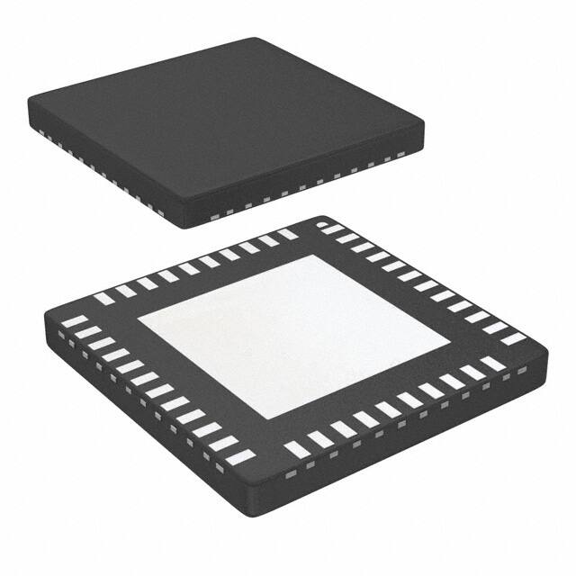
Product Offered in 44 Pin WQFN Package
High Impedance Bus Pins on Power Off
(VCC = 0 V)
2 Applications
The driver translates 3-V LVTTL levels (single-ended)
to differential Bus LVDS (BLVDS) output levels. This
allows for high speed operation while consuming
minimal power and reducing EMI. In addition, the
differential signaling provides common mode noise
rejection greater than ±1 V.
The receiver threshold is less than +0/−70 mV. The
receiver translates the differential Bus LVDS to
standard (LVTTL/LVCMOS) levels. (See the
Application Information Section for more details.)
Device Information(1)
PART NUMBER
DS92LV040A
PACKAGE
WQFN (44)
BODY SIZE (NOM)
7.00 mm x 7.00 mm
(1) For all available packages, see the orderable addendum at
the end of the data sheet.
Simplified Functional Diagram
DO1+/RI1+
DIN1
DO1-/RI1DE1
RO1
RE1
DO2+/RI2+
DIN2
DO2-/RI2-
Designed for Double Termination Applications
RO2
3 Description
The DS92LV040A is one in a series of Bus LVDS
transceivers designed specifically for high speed, low
power backplane or cable interfaces. The device
operates from a single 3.3-V power supply and
includes four differential line drivers and four
receivers. To minimize bus loading, the driver outputs
and receiver inputs are internally connected. The
device also features a flow through pin out which
allows easy PCB routing for short stubs between its
pins and the connector.
DO3+/RI3+
DIN3
DO3-/RI3DE2
RO3
RE2
DO4+/RI4+
DIN4
DO4-/RI4-
RO4
Copyright © 2018, Texas Instruments Incorporated
1
An IMPORTANT NOTICE at the end of this data sheet addresses availability, warranty, changes, use in safety-critical applications,
intellectual property matters and other important disclaimers. PRODUCTION DATA.
�DS92LV040A
SNOS521E – JANUARY 2001 – REVISED JANUARY 2018
www.ti.com
Table of Contents
1
2
3
4
5
6
Features ..................................................................
Applications ...........................................................
Description .............................................................
Revision History.....................................................
Pin Configuration and Functions .........................
Specifications.........................................................
1
1
1
2
3
4
6.1
6.2
6.3
6.4
6.5
6.6
4
4
4
4
5
6
Absolute Maximum Ratings ......................................
ESD Ratings..............................................................
Recommended Operating Conditions.......................
Thermal Information ..................................................
DC Electrical Characteristics ....................................
AC Electrical Characteristics.....................................
7
Parameter Measurement Information .................. 6
8
Detailed Description .............................................. 9
7.1 Test Circuits and Timing Waveforms ........................ 6
8.1 Overview ................................................................... 9
8.2 Functional Block Diagram ......................................... 9
8.3 Feature Description................................................... 9
8.4 Device Functional Modes........................................ 10
9
Application and Implementation ........................ 11
9.1 Application Information............................................ 11
9.2 Typical Application ................................................. 11
10 Power Supply Recommendations ..................... 13
11 Layout................................................................... 14
11.1 Layout Guidelines ................................................. 14
11.2 Layout Example .................................................... 17
12 Device and Documentation Support ................. 19
12.1
12.2
12.3
12.4
12.5
12.6
Documentation Support ........................................
Receiving Notification of Documentation Updates
Community Resources..........................................
Trademarks ...........................................................
Electrostatic Discharge Caution ............................
Glossary ................................................................
19
19
19
19
19
19
13 Mechanical, Packaging, and Orderable
Information ........................................................... 19
4 Revision History
NOTE: Page numbers for previous revisions may differ from page numbers in the current version.
Changes from Revision D (April 2013) to Revision E
Page
•
Added Device Information table, ESD Ratings table, Feature Description section, Device Functional Modes,
Application and Implementation section, Power Supply Recommendations section, Layout section, Device and
Documentation Support section, and Mechanical, Packaging, and Orderable Information section ..................................... 1
•
Added "Driver Short Circuit Current Duration" to the Absolute Maximum Ratings ................................................................ 4
•
Deleted Note 4: "Only one output at a time should be shorted..." from the DC Electrical Characteristics table.................... 5
Changes from Revision C (April 2013) to Revision D
•
2
Page
Changed layout of National Data Sheet to TI format ............................................................................................................. 3
Submit Documentation Feedback
Copyright © 2001–2018, Texas Instruments Incorporated
Product Folder Links: DS92LV040A
�DS92LV040A
www.ti.com
SNOS521E – JANUARY 2001 – REVISED JANUARY 2018
5 Pin Configuration and Functions
NC
11
NC
12
NC
RO4
DIN4
RO3
DIN3
GND
RO2
DIN2
RO1
DIN1
43
42
41
40
39
38
37
36
35
22
10
AVCC
AVCC
21
9
DO1+/RI1+
AGND
20
8
DO1í RI1í
DE34
19
7
DO2+/RI2+
AVCC
18
6
DO2í RI2í
VCC
17
5
AGND
RE34
16
4
DO3+/RI3+
GND
15
3
DO3í RI3í
VCC
14
2
DO4+/RI4+
NC
13
1
DO4í RI4í
NC
44
NJN Package
WQFN (44 Pin)
Top View
34
NC
33
NC
32
NC
31
GND
30
VCC
29
RE12
28
GND
27
AVCC
26
DE12
25
AGND
24
NC
23
NC
Not to scale
Pin Functions
PIN NAME
PIN #
INPUT/
OUTPUT
DO+/RI+
14, 16, 19, 21
I/O
True Bus LVDS Driver Outputs and Receiver Inputs.
DO−/RI−
13, 15, 18, 20
I/O
Complimentary Bus LVDS Driver Outputs and Receiver Inputs.
DIN
35, 37, 40, 42
I
LVTTL Driver Input. No pull up or pull down is attached to this pin
RO
36, 38, 41, 43
O
LVTTL Receiver Output.
RE12
29
I
Receiver Enable LVTTL Input (Active Low). This pin, when low, configures receiver outputs, RO1 and
RO2 active. When this pin is high, RO1 and RO2 are TRI-STATE. If this pin is floating, a weak current
source to VCC causes RO1 and RO2 to be TRI-STATE
RE34
5
I
Receiver Enable LVTTL Input (Active Low). This pin, when low, configures receiver outputs, RO3 and
RO4 active. When this pin is high, RO3 and RO4 are TRI-STATE. If this pin is floating, a weak current
source to VCC causes RO3 and RO4 to be TRI-STATE
DE12
26
I
Driver Enable LVTTL Input (Active High). This pin, when high, configures driver outputs, DO1+/RIN1+,
DO1−/RIN1− and DO2+/RIN2+, DO2−/RIN2− active. When this pin is low, driver outputs 1 and 2 are
TRI-STATE. If this pin is floating, a weak current source to VCC causes driver outputs 1 and 2 to be
active
DE34
8
I
Driver Enable LVTTL Input (Active High). This pin, when high, configures driver outputs, DO3+/RIN3+,
DO3−/RIN3− and DO4+/RIN4+, DO4−/RIN4− active. When this pin is low, driver outputs 3 and 4 are
TRI-STATE. If this pin is floating, a weak current source to VCC causes driver outputs 3 and 4 to be
active
GND
4, 28, 31, 39
Ground
Ground for digital circuitry (must connect to GND on PC board). These pins connected internally.
VCC
3, 6, 30
Power
VCC for digital circuitry (must connect to VCC on PC board). These pins connected internally.
AGND
9, 17, 25
Ground
Ground for analog circuitry (must connect to GND on PC board). These pins connected internally.
AVCC
7, 10, 22, 27
Power
Analog VCC (must connect to VCC on PC board). These pins connected internally.
NC
1, 2, 11, 12, 23, 24,
32, 33, 34, 44
N/A
Reserved for future use, leave open circuit.
GND
Must connect to GND plane through vias to achieve the theta ja specified under Absolute Maximum
Ratings. The DAP (die attach pad) is the heat transfer material that is centered on the bottom of the
WQFN package. Refer to application note AN-1187 () for attachment details.
DAP
DESCRIPTIONS
Submit Documentation Feedback
Copyright © 2001–2018, Texas Instruments Incorporated
Product Folder Links: DS92LV040A
3
�DS92LV040A
SNOS521E – JANUARY 2001 – REVISED JANUARY 2018
www.ti.com
6 Specifications
6.1 Absolute Maximum Ratings
over operating free-air temperature range (unless otherwise noted) (1) (2)ccr (3)
MIN
MAX
UNIT
4
V
Supply Voltage, VCC
Enable Input Voltage (DE, RE)
−0.3
VCC +0.3 V
V
Driver Input Voltage (DIN)
−0.3
VCC +0.3 V
V
Driver Short Circuit Current Duration
Continuous
Receiver Output Voltage ( ROUT)
−0.3
VCC +0.3 V
Bus Pin Voltage (DO±/RI±)
−0.3
3.9
V
Storage temperature, Tstg
−65
150
°C
(1)
(2)
(3)
V
Stresses beyond those listed under Absolute Maximum Ratings may cause permanent damage to the device. These are stress ratings
only, which do not imply functional operation of the device at these or any other conditions beyond those indicated under Recommended
Operating Conditions. Exposure to absolute-maximum-rated conditions for extended periods may affect device reliability.
If Military/Aerospace specified devices are required, please contact the Texas Instruments Sales Office/ Distributors for availability and
specifications.
All currents into device pins are positive; all currents out of device pins are negative. All voltages are referenced to ground unless
otherwise specified except VOD, ΔVOD and VID.
6.2 ESD Ratings
VALUE
Electrostatic discharge (1) (2)
V(ESD)
(1)
(2)
(3)
(4)
Human-body model (HBM), per ANSI/ESDA/JEDEC JS-001 (3)
±2000
Charged-device model (CDM), per JEDEC specification JESD22C101 (4)
±1000
UNIT
V
All typicals are given for VCC = +3.3 V and TA = +25°C, unless otherwise stated.
ESD Rating: HBM (1.5 kΩ, 100 pF) > 4 kV EIAJ (0 Ω, 200 pF) > 250.
JEDEC document JEP155 states that 500-V HBM allows safe manufacturing with a standard ESD control process.
JEDEC document JEP157 states that 250-V CDM allows safe manufacturing with a standard ESD control process.
6.3 Recommended Operating Conditions
over operating free-air temperature range (unless otherwise noted)
MIN
VCC
TA
MAX
UNIT
Supply Voltage
3
3.6
Receiver Input Voltage
0
2.4
V
−40
85
°C
Data
1
ns/V
Control
3
ns/V
Ambient Free Air Temperature
Slowest Input Edge Rate, Δt/ΔV
(20% to 80%) (1)
(1)
NOM
V
Generator waveforms for all tests unless otherwise specified: f = 25 MHz, ZO = 50 Ω, tr, tf =
Typical 12-Layer PCB
Figure 17. Low Inductance, High-Capacitance Power Connection
Bypass capacitors should be placed close to VDD pins. They can be placed conveniently near the corners or
underneath the package to minimize the loop area. This extends the useful frequency range of the added
capacitance. Small-physical-size capacitors, such as 0402, 0201, or X7R surface-mount capacitors should be
used to minimize body inductance of capacitors. Each bypass capacitor is connected to the power and ground
plane through vias tangent to the pads of the capacitor as shown in Figure 18(a).
16
Submit Documentation Feedback
Copyright © 2001–2018, Texas Instruments Incorporated
Product Folder Links: DS92LV040A
�DS92LV040A
www.ti.com
SNOS521E – JANUARY 2001 – REVISED JANUARY 2018
Layout Guidelines (continued)
An X7R surface-mount capacitor of size 0402 has about 0.5 nH of body inductance. At frequencies above 30
MHz or so, X7R capacitors behave as low-impedance inductors. To extend the operating frequency range to a
few hundred MHz, an array of different capacitor values like 100 pF, 1 nF, 0.03 μF, and 0.1 μF are commonly
used in parallel. The most effective bypass capacitor can be built using sandwiched layers of power and ground
at a separation of 2 to 3 mils. With a 2-mil FR4 dielectric, there is approximately 500 pF per square inch of PCB.
Many high-speed devices provide a low-inductance GND connection on the backside of the package. This center
pad must be connected to a ground plane through an array of vias. The via array reduces the effective
inductance to ground and enhances the thermal performance of the small Surface Mount Technology (SMT)
package. Placing vias around the perimeter of the pad connection ensures proper heat spreading and the lowest
possible die temperature. Placing high-performance devices on opposing sides of the PCB using two GND
planes creates multiple paths for heat transfer. Often thermal PCB issues are the result of one device adding
heat to another, resulting in a very high local temperature. Multiple paths for heat transfer minimize this
possibility. In many cases the GND pad makes the optimal decoupling layout impossible to achieve due to
insufficient pad-to-pad spacing as shown in Figure 18(b). When this occurs, placing the decoupling capacitor on
the backside of the board keeps the extra inductance to a minimum. It is important to place the VDD via as close
to the device pin as possible while still allowing for sufficient solder mask coverage. If the via is left open, solder
may flow from the pad and into the via barrel. This results in a poor solder connection.
(a)
(b)
VDD
0402
IN±
IN+
0402
Figure 18. Typical Decoupling Capacitor Layouts
11.2 Layout Example
At least two or three times the width of an individual trace should separate single-ended traces and differential
pairs to minimize the potential for crosstalk. Single-ended traces that run in parallel for less than the wavelength
of the rise or fall times usually have negligible crosstalk. Increase the spacing between signal paths for long
parallel runs to reduce crosstalk. Boards with limited real estate can benefit from the staggered trace layout, as
shown in Figure 19.
Layer 1
Layer 6
Figure 19. Staggered Trace Layout
Submit Documentation Feedback
Copyright © 2001–2018, Texas Instruments Incorporated
Product Folder Links: DS92LV040A
17
�DS92LV040A
SNOS521E – JANUARY 2001 – REVISED JANUARY 2018
www.ti.com
Layout Example (continued)
This configuration lays out alternating signal traces on different layers; thus, the horizontal separation between
traces can be less than 2 or 3 times the width of individual traces. To ensure continuity in the ground signal path,
TI recommends having an adjacent ground via for every signal via, as shown in Figure 20. Note that vias create
additional capacitance. For example, a typical via has a lumped capacitance effect of 1/2 pF to 1 pF in FR4.
Signal Via
Signal Trace
Uninterrupted Ground Plane
Signal Trace
Uninterrupted Ground Plane
Ground Via
Figure 20. Ground Via Location (Side View)
Short and low-impedance connection of the device ground pins to the PCB ground plane reduces ground
bounce. Holes and cutouts in the ground planes can adversely affect current return paths if they create
discontinuities that increase returning current loop areas.
To minimize EMI problems, TI recommends avoiding discontinuities below a trace (for example, holes, slits, and
so on) and keeping traces as short as possible. Zoning the board wisely by placing all similar functions in the
same area, as opposed to mixing them together, helps reduce susceptibility issues.
18
Submit Documentation Feedback
Copyright © 2001–2018, Texas Instruments Incorporated
Product Folder Links: DS92LV040A
�DS92LV040A
www.ti.com
SNOS521E – JANUARY 2001 – REVISED JANUARY 2018
12 Device and Documentation Support
12.1 Documentation Support
12.1.1 Related Documentation
General application guidelines and hints may be found in the following application notes: ), A).
For related documentation see the following:
• AN-808 (SNLA028)
• AN-977 (SNLA166
• AN-971 (SNLA165)
• AN-903 (SNLA034
12.2 Receiving Notification of Documentation Updates
To receive notification of documentation updates, navigate to the device product folder on ti.com. In the upper
right corner, click on Alert me to register and receive a weekly digest of any product information that has
changed. For change details, review the revision history included in any revised document.
12.3 Community Resources
The following links connect to TI community resources. Linked contents are provided "AS IS" by the respective
contributors. They do not constitute TI specifications and do not necessarily reflect TI's views; see TI's Terms of
Use.
TI E2E™ Online Community TI's Engineer-to-Engineer (E2E) Community. Created to foster collaboration
among engineers. At e2e.ti.com, you can ask questions, share knowledge, explore ideas and help
solve problems with fellow engineers.
Design Support TI's Design Support Quickly find helpful E2E forums along with design support tools and
contact information for technical support.
12.4 Trademarks
E2E is a trademark of Texas Instruments.
Rogers is a trademark of Rogers Corporation.
All other trademarks are the property of their respective owners.
12.5 Electrostatic Discharge Caution
This integrated circuit can be damaged by ESD. Texas Instruments recommends that all integrated circuits be handled with
appropriate precautions. Failure to observe proper handling and installation procedures can cause damage.
ESD damage can range from subtle performance degradation to complete device failure. Precision integrated circuits may be more
susceptible to damage because very small parametric changes could cause the device not to meet its published specifications.
12.6 Glossary
SLYZ022 — TI Glossary.
This glossary lists and explains terms, acronyms, and definitions.
13 Mechanical, Packaging, and Orderable Information
The following pages include mechanical, packaging, and orderable information. This information is the most
current data available for the designated devices. This data is subject to change without notice and revision of
this document. For browser-based versions of this data sheet, refer to the left-hand navigation.
Submit Documentation Feedback
Copyright © 2001–2018, Texas Instruments Incorporated
Product Folder Links: DS92LV040A
19
�PACKAGE OPTION ADDENDUM
www.ti.com
10-Dec-2020
PACKAGING INFORMATION
Orderable Device
Status
(1)
Package Type Package Pins Package
Drawing
Qty
Eco Plan
(2)
Lead finish/
Ball material
MSL Peak Temp
Op Temp (°C)
Device Marking
(3)
(4/5)
(6)
DS92LV040ATLQA/NOPB
ACTIVE
WQFN
NJN
44
250
RoHS & Green
SN
Level-2-260C-1 YEAR
-40 to 85
LV040A
DS92LV040ATLQAX/NOPB
ACTIVE
WQFN
NJN
44
2500
RoHS & Green
SN
Level-2-260C-1 YEAR
-40 to 85
LV040A
(1)
The marketing status values are defined as follows:
ACTIVE: Product device recommended for new designs.
LIFEBUY: TI has announced that the device will be discontinued, and a lifetime-buy period is in effect.
NRND: Not recommended for new designs. Device is in production to support existing customers, but TI does not recommend using this part in a new design.
PREVIEW: Device has been announced but is not in production. Samples may or may not be available.
OBSOLETE: TI has discontinued the production of the device.
(2)
RoHS: TI defines "RoHS" to mean semiconductor products that are compliant with the current EU RoHS requirements for all 10 RoHS substances, including the requirement that RoHS substance
do not exceed 0.1% by weight in homogeneous materials. Where designed to be soldered at high temperatures, "RoHS" products are suitable for use in specified lead-free processes. TI may
reference these types of products as "Pb-Free".
RoHS Exempt: TI defines "RoHS Exempt" to mean products that contain lead but are compliant with EU RoHS pursuant to a specific EU RoHS exemption.
Green: TI defines "Green" to mean the content of Chlorine (Cl) and Bromine (Br) based flame retardants meet JS709B low halogen requirements of


 工商网监
湘ICP备2023018690号
工商网监
湘ICP备2023018690号
