July 2004
FPD87346BXA
Low EMI, Low Dynamic Power (SVGA) XGA/WXGA
TFT-LCD Timing Controller with Reduced Swing
Differential Signaling (RSDS™) Outputs
General Description
Features
The FPD87346BXA is a timing controller that combines an
LVDS single pixel input interface with National’s Reduced
Swing Differential Signaling (RSDS™) output driver interface
for (SVGA) XGA and Wide XGA resolutions. It resides on the
TFT-LCD panel and provides the data buffering and control
signal generation for (SVGA) XGA, and Wide XGA graphic
modes. The RSDS™ path to the column driver contributes
toward lowering radiated EMI and reducing system dynamic
power consumption.
This single RSDS™ bus conveys the 8-bit color data for
(SVGA) XGA, and Wide XGA panels at 170 Mb/s when using
VESA 60 Hz standard timing.
n Reduced Swing Differential Signalling (RSDS™) digital
bus reduces dynamic power, EMI and bus width from
the timing controller
n LVDS single pixel input interface system
n Input clock range from 40 MHz to 85 MHz
n Drives RSDS™ Column Drivers at 170 Mb/s with an
85 MHz clock (Max.)
n Virtual 8 bit color depth in FRC/Dithering mode
n Single narrow 9-bit differential Source Driver bus
minimizes width of Source PCB
n Ability to drive (SVGA) XGA and Wide XGA TFT-LCD
Systems
n Failure detect function in DE mode (Bonding Option)
n CMOS circuitry operates from a 3.0V–3.6V supply
System Diagram
20101601
FIGURE 1. Block Diagram of the LCD Module
RSDS™ is a trademark of National Semiconductor Corporation
© 2004 National Semiconductor Corporation
DS201016
www.national.com
FPD87346BXA Low EMI, Low Dynamic Power (SVGA) XGA/WXGA TFT-LCD Timing Controller
with Reduced Swing Differential Signaling (RSDS™) Outputs
PRELIMINARY
�FPD87346BXA
Block Diagram
20101620
FIGURE 2. Block Diagram
Functional Description
DATAPATH BLOCK AND RSDS™ TRANSMITTER
6(8)-bit video data (RGB) is input to the Datapath Block
supports up to an 85 MHz pixel rate. The data is delayed to
align the Column Driver Start Pulse with the Column Driver
data. The data bus (RSR[2:0]P/N, RSG[2:0]P/N, RSB[2:0]P/
N) outputs at a 170 MHz rate on 9 differential output channels. The clock is output on the RSCKP/N differential pair.
The RSDS Column Drivers latch data on both positive and
negative edges of the clock. The RSDS™ output setup/hold
timings are also adjustable through the RSDS[2:0] input
pins.
FPD-LINK RECEIVER
The FPD87346BXA is TFT-LCD Timing Controller (TCON)
that is based on National Semiconductor’s Embedded Logic
Array family of TCON devices. The logic architecture is
implemented using standard and default timing controller
functionality based on an Embedded Gate Array. In it’s standard configuration the Gate Driver Control, Column Driver
Control signals, and Logic Functions of the device are preset. Customization of control signal timing and other logic
functions of the device are reconfigurable through customer
supplied Verilog/RTL Code or User-defined specifications.
The combination of Embedded Logic Array and National
Semiconductor’s world class Mixed-signal Analog functional
blocks such as LVDS and RSDS™ provides a flexible platform to meet the needs of TFT-LCD Manufacturers.
TIMING CONTROL FUNCTION
The Timing Controller Functional Block generates all the
necessary control signals to the Column Driver (TP, STH,
and REV) and Gate Drivers (STV, CPV, and OE) to interface
with a TFT-LCD panel.
SPREAD SPECTRUM SUPPORT
The FPD-Link receiver supports graphics controllers with
Spread Spectrum interfaces for reducing EMI. The Spread
Spectrum methods supported are center and down spread.
A maximum of deviation of ± 2% center spread or -4% down
spread is supported at a frequency modulation of 100 kHz
maximum.
RSDS OUTPUT VOLTAGE CONTROL
The RSDS™ output voltage swing is controlled through an
external load resistor connected to the RPI pin. The RSDS™
output signal levels can be adjusted to suit the particular
application. This is dependent on overall LCD module design
characteristics such as trace impedance, termination, etc.
The RSDS™ output voltage is inversely related to the RPI
value. Lower RPI values will increase the RSDS™ output
voltage swing and consequently overall power consumption
will also increase.
8-6 BIT TRANSLATOR
8-bit data is reduced to a 6-bit data path via a time multiplexed dithering technique or simple truncation of the LSBs.
This function is enabled via the input control pins.
www.national.com
2
�ESD Rating:
(CZAP = 120 pF,
If Military/Aerospace specified devices are required,
please contact the National Semiconductor Sales Office/
Distributors for availability and specifications.
Supply Voltage (VDD)
−0.3V to (VDD + 0.3V)
DC Output Voltage (VOUT)
−0.3V to (VDD + 0.3V)
Junction Temperature
Operating Conditions
Supply Voltage (VDD)
+150˚C
Storage Temperature Range
(TSTG)
MM = 200V,
HBM = 2000V
−0.3V to +4.0V
DC TTL Input Voltage (VIN)
RZAP = 1500Ω)
Operating Temp Range (TA)
Min
Max
3.0
3.6
V
0
70
˚C
200
mVPP
Supply Noise Voltage (VDD)
−65˚C to +150˚C
Units
Spread Spectrum Support, LVDS
Lead Temperature (TL)
(Soldering 10 sec.)
260˚C
Spreading Range
± 2.0
%
Modulation Rate
100
kHz
85
MHz
Operating Frequency (f)
40
DC Electrical Characteristics
TA = 0˚C to 70˚C, VDD = 3.3V ± 0.3V, IPI = 100 µA (Unless otherwise specified).
TTL DC ELECTRICAL CHARACTERISTICS
Symbol
VOH
VOL
Parameter
Minimum High Level Output
Voltage
Maximum Low Level Output
Voltage
Conditions
STV, CPV, OE
Min
Typ
Max
Units
IOH = -6 mA
TP, REV
IOH = -8 mA
STH
IOH = -24 mA
STV, CPV, OE
IOL = +6 mA
TP, REV
IOL = +8 mA
STH
IOL = +24 mA
VIH
Minimum High Level Input Voltage
VIL
Maximum Low Level Input Voltage
IIN
Input Current
VIN = VDD, GND
IDD
Average Supply Current
f = 85 MHz
VDD = 3.6V, CL(TTL) = 15 pF,
IPI = 100 µA (Typically PI pin
connected to 13 kΩ to ground)
RL(RSDS) = 100Ω and
CL(RSDS) = 5 pF
(jig & test fixture capacitance),
See Figure 3 for input conditions
2.4
V
0.4
2.0
V
V
–10
85
0.8
V
+10
µA
150
mA
Note 1: “Absolute Maximum Rating” are those values beyond which the safety of the device cannot be guaranteed. They are not meant to imply that the devices
should be operated at these limits. The table of “Electrical Characteristics” specifies conditions of device operation.
3
www.national.com
FPD87346BXA
Absolute Maximum Ratings (Note 1)
�FPD87346BXA
DC Electrical Characteristics
TA = 0˚C to 70˚C, VDD = 3.3V ± 0.3V, IPI = 100 µA (Unless otherwise specified). (Continued)
FPD-Link Receiver Input Pattern Used to Measure IDD
20101602
FIGURE 3. FPD-Link Receiver IDD Pattern
FPD-Link (LVDS) RECEIVER INPUT (RxCLK+/-, RxIN[y]+/-; y = 0, 1, 2, 3)
Symbol
Parameter
Conditions
Min
Typ
Max
Units
+100
mV
LVDS RECEIVER DC SPECIFICATIONS (Note 2)
VTHLVDS
Differential Input High Threshold
Voltage
VTLLVDS
Differential Input Low Threshold
Voltage
IIN
Input Current
VIN
Input Voltage Range (Single-ended)
|VID|
Differential Input Voltage
VCM
Common Mode Voltage Offset
VCM = 1.2V
–100
mV
VIN = 2.4V, VDD = 3.6V
–10
+10
µA
VIN = 0V, VDD = 3.6V
–10
+10
µA
0
2.4
V
0.100
0.600
V
0+|VID|/2
2.4−|VID|/2
V
Note 2: LVDS Receiver DC parameters are measured under static and steady state conditions which may not reflect the actual performance in the end application.
|VID| and VCM Definitions Using Single-End Signals
20101603
FIGURE 4. |VID| and VCM Allowable Operating Range
www.national.com
4
�TA = 0˚C to 70˚C, VDD = 3.3V ± 0.3V, IPI = 100 µA (Unless otherwise specified). (Continued)
RSDS TRANSMITTER OUTPUT (RSCKP/N, RSx[y]P/N; x = R, G, B y = 0, 1, 2)
Symbol
VODRSDS
VOSRSDS
Parameter
Conditions
Differential Output Voltage
Min
Typ
Max
Units
± 200
RL = 100Ω
RPI = 13 kΩ
(Note 3) and
(Figure 5)
Offset Voltage
1.1
1.3
mV
1.5
V
Note 3: VOSRSDS = (V(F&B)CLKP + V(F&B)CLKN)/2 or VOSRSDS = (V(F&B)XYP + V(F&B)XYN)/2.
VODRSDS = V(F&B)CLKP − V(F&B)CLKN or VODRSDS = V(F&B)XYP − V(F&B)XYN.
The load between the positive and negative output is 100Ω.
20101604
FIGURE 5. RSDS Waveform - Single Ended and Differential
20101619
FIGURE 6. Typical RSDSVOD vs. RPI Response Curve
5
www.national.com
FPD87346BXA
DC Electrical Characteristics
�FPD87346BXA
AC Electrical Characteristics
TA = 0˚C to 70˚C, VDD = 3.3V ± 0.3V, IPI = 100 µA (Unless otherwise specified).
LVDS Data Input
Symbol
Parameter
Conditions
RSCLKOUTDLY
FPD-Link Receiver Phase Lock Loop Wake-up
Time
Figure 9
RSKM
RxIN Skew Margin (Note 4) and (Figure 7)
f = 85 MHz, VDD = 3.3V
Min
Max
Units
10
ms
220
ps
Note 4: Receiver Skew Margin is defined as the valid data sampling region at the receiver inputs.
This margin takes into account transmitter pulse positions (min and max) and the receiver input setup and hold time (internal data sampling window: RSPOS). This
margin allows for LVDS interconnect skew, inter-symbol interference (both dependent on type and length of cable, and source clock (FPD-Link Transmitter TxCLK
IN) jitter (less than 190 ps). The specified RSKM minimum assumes a TPPOS max of 200 ps.
RSKM = cable skew (type, length) + source clock jitter (cycle to cycle) + remaining margin for data sampling (≥0)
This parameter is guaranteed by design. The limits are based on statistical analysis of the device performance over PVT (Process, Voltage, Temperature) range.
20101605
FIGURE 7. FPD87346BXA (FPD-Link Receiver) Input Skew Margin
www.national.com
6
�FPD87346BXA
AC Electrical Characteristics
TA = 0˚C to 70˚C, VDD = 3.3V ± 0.3V, IPI = 100 µA (Unless otherwise specified). (Continued)
20101606
Note 5: R/G/B[7]s are MSBs and R/G/B/[0]s are LSBs
FIGURE 8. FPD87346BXA (FPD-Link Receiver) Input Data Mapping
20101607
FIGURE 9. FPD87346BXA (FPD-Link Receiver) Phase Lock Loop Wake-up Time
7
www.national.com
�FPD87346BXA
AC Electrical Characteristics
TA = 0˚C to 70˚C, VDD = 3.3V ± 0.3V, IPI = 100 µA (Unless otherwise specified). (Continued)
Output Timing
Symbol
TO1
Parameter
Conditions
Min
Typ
Max
Units
0.0
11.25
ns
0.0
11.25
ns
TTL Output Rising from RSCLK
Rising
CL(TTL) = 15 pF, RT = 100Ω,
CL(RSDS) = 5 pF, IPI = 100 µA,
f = 85 MHz
TTL Output Falling from RSCK
Rising
CL(TTL) = 15 pF, RT = 100Ω,
CL(RSDS) = 5 pF, IPI = 100 µA,
f = 85 MHz
RCHP
RSDS Clock (RSCK) High Period
RT = 100Ω, CL(RSDS) = 5 pF,
IPI = 100 µA, f = 85 MHz
5.7
ns
RCLP
RSDS Clock (RSCK) Low Period
RT = 100Ω, CL(RSDS) = 5 pF,
IPI = 100 µA, f = 85 MHz
5.8
ns
RSTU
RS(R,G,B) Setup to Falling or
Rising Edge of RSCK
RT = 100Ω, CL(RSDS) = 5 pF,
IPI = 100 µA, f = 85 MHz,
RSDS[2:0] = [000]
3.2
ns
RS(R,G,B) Hold from Falling or
Rising Edge of RSCK
RT = 100Ω, CL(RSDS) = 5 pF,
IPI = 100 µA, f = 85 MHz,
RSDS[2:0] = [000]
1.8
ns
SPSTU
STH Rising to RSCK Falling
RT = 100Ω, CL(RSDS) = 5 pF,
IPI = 100 µA, f = 85 MHz
5.0
ns
SPHLD
STH Falling to RSCK Falling
RT = 100Ω, CL(RSDS) = 5 pF,
IPI = 100 µA, f = 85 MHz
4.0
ns
TO2
RHLD
TABLE 1.
Typical Simulation Results of RSDS Skew Control Values* (VDD = 3.3V; RT = 100ohms; IPI = 100 µA; 25˚C)
RSDS[2:0]
f = 65 MHz
f = 85 MHz
RSTU
RHLD
RSTU
RHLD
000
5.03
1.83
3.23
1.83
001
5.26
1.31
3.75
1.31
010
6.03
0.83
4.23
0.83
011
6.53
0.33
4.73
0.33
100
3.01
3.77
1.21
3.77
101
3.49
3.33
1.69
3.33
110
4.00
2.86
2.20
2.86
111
4.50
2.36
2.70
2.36
Unit
ns
ns
*The skew control value in the table are only sampling values of a specific condition and is not a parametric value. Typical values on this table are measured under
Static and Steady state conditions which may not be reflective of its performance in the end application.
www.national.com
8
�FPD87346BXA
AC Electrical Characteristics
TA = 0˚C to 70˚C, VDD = 3.3V ± 0.3V, IPI = 100 µA (Unless otherwise specified). (Continued)
20101608
20101610
20101609
FIGURE 10. FPD87346BXA RSDS and TTL Output Timing Diagram
9
www.national.com
�FPD87346BXA
AC Electrical Characteristics
TA = 0˚C to 70˚C, VDD = 3.3V ± 0.3V, IPI = 100 µA (Unless otherwise specified). (Continued)
20101611
Note: RSCKP/N, RSR[2:0]P/N, RSG[2:0]P/N and RSB[2:0]P/N are differential outputs, STH is a single ended TTL output.
FIGURE 11. FPD87346BXA RSDS Output Data Mapping
www.national.com
10
�TA = 0˚C to 70˚C, VDD = 3.3V ± 0.3V, IPI = 100 µA (Unless otherwise specified). (Continued)
FPD87346BXA Failure Detect (Internal Bonding Option)
This function is valid in DE mode. As shown in Figure 12, invalid external DE pulse will not affect the internal operation during
failure zone.
20101612
FIGURE 12. FPD87346BXA Failure Detection
11
www.national.com
FPD87346BXA
AC Electrical Characteristics
�FPD87346BXA
Input Signal Timing
Signal
Item
Symbol
Clock Frequency
1/Tclk
f
Total
Tv
Vertical Timing
Active
Tvact
Total
Th
Horizontal Timing
Active
Thact
SVGA
(800 x 600)
XGA
(1024 x 768)
WXGA I
(1280 x 768)
WXGA II
(1280 x 800)
Unit
MHz
typ
40
65
82
69
min
620
772
772
804
typ
628
806
806
816
max
664
850
850
900
min
–
–
–
–
typ
600
768
768
800
max
–
–
–
–
min
1050
1050
1320
1320
typ
1056
1344
1688
1408
max
1056
1800
2000
2000
min
–
–
–
–
typ
800
1024
1280
1280
max
–
–
–
–
Th
Tclk
Output Timing—TTL
DE (Data Enable) Mode Only
Display Mode WIDE(0/1) (Pin 57)
Parameter
Comments
SVGA
(WIDE=0)
XGA
(WIDE=0)
WXGA
(WIDE=1)
Remarks/
Unit
RxCLKP/N
t1
STH Rising to Active Data
2
2
2
t2
High Duration of STH
1
1
1
RxCLKP/N
t3
STH Rising to TP
1031
1031
1285
RxCLKP/N
t4
High Duration of TP
8
8
10
RxCLKP/N
t5
STH Rising to OE
904
904
1147
RxCLKP/N
t6
High Duration of OE
159
159
180
RxCLKP/N
t7
STH Rising to CPV
1031
1031
1283
RxCLKP/N
t8
High Duration of CPV
684
684
724
RxCLKP/N
t9
STH Rising to STV
368
368
565
RxCLKP/N
H Line (Note 6)
t10
High Duration of STV
t11
STH Rising to REV (1HRVS)
t12
High/Low Duration of REV (1HRVS)
t13
STH Rising to REV (2HRVS)
t14
High/Low Duration of REV (2HRVS)
Note 6: H Line: Hsync Cycle
www.national.com
12
1
1
1
390
390
567
RxCLKP/N
1
1
1
H Line (Note 6)
371
371
567
RxCLKP/N
2
2
2
H Line (Note 6)
�FPD87346BXA
Output Timing—TTL
(Continued)
20101613
FIGURE 13. FPD87346BXA TTL Output Timing Diagram
13
www.national.com
�FPD87346BXA
Output Timing—TTL
(Continued)
20101614
FIGURE 14. FPD87346BXA TTL Output Timing Diagram (continued)
www.national.com
14
�(Continued)
TABLE 2.
ROn (Sn) Configuration (TA = 25˚C; XGA: RxCLKP/N = 65 MHz; WXGA: RxCLKP/N = 85 MHz)
OE
RO2
(S2)
RO1
(S1)
RO0
(S0)
REV
0
0
0
1HRVS
0
0
1
2HRVS
0
1
0
2HRVS
0
1
1
1HRVS
1
0
0
2HRVS
1
0
1
1
1
0
1
1
1
2HRVS
TP
XGA
(Front)
WXGA
(Back)
2.4
2.1
XGA
WXGA
0.12
0.12
0.12
0.12
0.25
0.50
0.12
0.12
0.12
0.12
2HRVS
0.25
0.50
1HRVS
0.25
0.50
0.25
0.50
2.9
3.4
2.6
3.1
Unit
µs
20101616
20101617
FIGURE 15. FPD87346BXA ROn (Sn) Configuration Timing Diagrams
15
www.national.com
FPD87346BXA
Output Timing—TTL
�FPD87346BXA
Pin Connection
20101618
FIGURE 16. Pinout Assignments
Pin Description
System Interface
Symbol
Pin
Type
Function
RxIN[0]P/N
3, 4
LVDSI
FPD-Link Data Differential Pair 0 Input
RxIN[1]P/N
5, 6
LVDSI
FPD-Link Data Differential Pair 1 Input
RxIN[2]P/N
7, 8
LVDSI
FPD-Link Data Differential Pair 2 Input
RxIN[3]P/N
11, 12
LVDSI
FPD-Link Data Differential Pair 3 Input
RxCLKP/N
9, 10
LVDSI
PFD-Link Clock Differential Pair Input
Sub-Total
10
Pin Count
Column Driver Interface
Pin
Type
R[2:0]P/N
Symbol
26–31
RSO
Red Reduced Swing Differential Outputs to Column Drivers
G[2:0]P/N
36–41
RSO
Green Reduced Swing Differential Outputs to Column Drivers
B[2:0]P/N
42–47
RSO
Blue Reduced Swing Differential Outputs to Column Drivers
CLKP/N
34, 35
RSO
TP
50
TO, 8mA
Line Latch Signal Output to Column Drivers
STH
52
TO, 24mA
Horizontal Start Signal Output to Column Drivers
REV
51
TO, 8mA
Alternative Signal Output for each 1 or 2 Horizontal Line to Column Drivers
and LC Control
www.national.com
Function
Clock Reduced Swing Differential Outputs to Column Drivers
16
�FPD87346BXA
Pin Description
(Continued)
Column Driver Interface
Symbol
Pin
Type
Function
Sub-Total
23
Pin Count
Row Driver Interface
Pin
Type
STV
Symbol
53
TO, 6mA
Row Driver Start Pulse
CPV
54
TO, 6mA
Row Driver Shift Clock
OE
55
TO, 6mA
Control TFT Gate Pulse Width to Row Drivers
Sub-Total
Pin Count
Control Pins
3
Symbol
Function
Pin
Type
56
I
Data Dithering Option:
0: 8-Bit Input, Dithering (FRC)
1: 6-Bit Input, Non Dithering (No FRC)
20–22
I
RSDS Skew/Timing Control (See Table 1)
57
I
0: SVGA (800 x 600)
0: XGA (1024 x 768)
1: WXGA (1280 x 768/800)
60–62
I
Alternate each 1 Horizontal/2 Horizontal on REV with OE Timing
(See Table 2 and Figure 15)
RES
59
I
Reserved pin, tie to high (VDD)
TEST
23
I
0: Normal Operation
1: Test Mode
Sub-Total
Pin Count
Power Supply
10
FRC
RSDS[2:0]
WIDE
RO[2:0]
Symbol
Pin
Function
Type
Function
VDD
17
P
Digital Power for Logic Core and LVDS Deserializer
VSS
63
G
Digital Ground for Logic Core and LVDS Deserializer
VDDIO
18, 32, 48,
49
P
Digital I/O Power and RSDS Outputs
VSSIO
16, 25, 33,
64
G
Digital I/O Ground and RSDS Outputs
VDDA
1
P
Power for LVDS PLL and Analog Bandgap
VDDD
2
P
Digital Power for LVDS Input Buffer
VSSD
13
G
Digital Ground for LVDS Input Buffer
VSSP
15
G
Ground for LVDS PLL and Analog Bandgap
VSSA
14
G
Ground for LVDS PLL and Analog Bandgap
Sub-Total
Pin Count
15
17
www.national.com
�FPD87346BXA
Pin Description
(Continued)
Other
Pin
Type
PI
Symbol
24
I
Reference for Reduced Swing Differential Outputs
Function
RSTZ
19
I
System Reset; Active Low
NC
58
I
No Connect
Sub-Total
Pin Count
3
Total
Pin Count
64
System Interface = 10
Column Driver = 23
Row Driver = 3
Control Pins = 10
Power Supply = 15
Other = 3
Bonding Options (B/O)
Symbol
FAIL_ON
Pin
Type
B/O
PD
Function
Failure Detect Function ON/OFF
Low : OFF (Default)
High : ON
Pin Types
I
TO
LVDSI
RSO
P
G
B/O
-Input (LVTTL-Compatible)
-TTL Output (LVTTL-Compatible)
-Low Voltage Differential Signal Input
-Reduced Swing Differential Output
-Power
-Ground
-Bonding Option
PD
PU
-Internal Pull-Down
-Internal Pull-Up
www.national.com
18
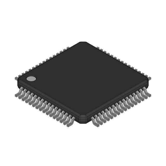
�inches (millimeters) unless otherwise noted
64-pin TQFP Package
Order Number FPD87346BXAVS
NS Package Number VEC-64A
LIFE SUPPORT POLICY
NATIONAL’S PRODUCTS ARE NOT AUTHORIZED FOR USE AS CRITICAL COMPONENTS IN LIFE SUPPORT
DEVICES OR SYSTEMS WITHOUT THE EXPRESS WRITTEN APPROVAL OF THE PRESIDENT AND GENERAL
COUNSEL OF NATIONAL SEMICONDUCTOR CORPORATION. As used herein:
1. Life support devices or systems are devices or
systems which, (a) are intended for surgical implant
into the body, or (b) support or sustain life, and
whose failure to perform when properly used in
accordance with instructions for use provided in the
labeling, can be reasonably expected to result in a
significant injury to the user.
2. A critical component is any component of a life
support device or system whose failure to perform
can be reasonably expected to cause the failure of
the life support device or system, or to affect its
safety or effectiveness.
BANNED SUBSTANCE COMPLIANCE
National Semiconductor certifies that the products and packing materials meet the provisions of the Customer Products
Stewardship Specification (CSP-9-111C2) and the Banned Substances and Materials of Interest Specification
(CSP-9-111S2) and contain no ‘‘Banned Substances’’ as defined in CSP-9-111S2.
National Semiconductor
Americas Customer
Support Center
Email: new.feedback@nsc.com
Tel: 1-800-272-9959
www.national.com
National Semiconductor
Europe Customer Support Center
Fax: +49 (0) 180-530 85 86
Email: europe.support@nsc.com
Deutsch Tel: +49 (0) 69 9508 6208
English Tel: +44 (0) 870 24 0 2171
Français Tel: +33 (0) 1 41 91 8790
National Semiconductor
Asia Pacific Customer
Support Center
Email: ap.support@nsc.com
National Semiconductor
Japan Customer Support Center
Fax: 81-3-5639-7507
Email: jpn.feedback@nsc.com
Tel: 81-3-5639-7560
National does not assume any responsibility for use of any circuitry described, no circuit patent licenses are implied and National reserves the right at any time without notice to change said circuitry and specifications.
FPD87346BXA Low EMI, Low Dynamic Power (SVGA) XGA/WXGA TFT-LCD Timing Controller
with Reduced Swing Differential Signaling (RSDS™) Outputs
Physical Dimensions
�


 工商网监
湘ICP备2023018690号
工商网监
湘ICP备2023018690号
