®
INA101
High Accuracy
INSTRUMENTATION AMPLIFIER
FEATURES
●
●
●
●
●
●
●
APPLICATIONS
LOW DRIFT: 0.25µV/°C max
LOW OFFSET VOLTAGE: 25µV max
LOW NONLINEARITY: 0.002%
LOW NOISE: 13nV/√Hz
HIGH CMR: 106dB AT 60Hz
HIGH INPUT IMPEDANCE: 1010Ω
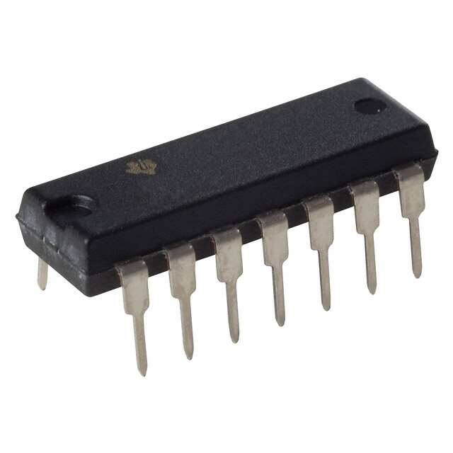
14-PIN PLASTIC, CERAMIC DIP,
SOL-16, AND TO-100 PACKAGES
●
●
●
●
●
●
STRAIN GAGES
THERMOCOUPLES
RTDs
REMOTE TRANSDUCERS
LOW-LEVEL SIGNALS
MEDICAL INSTRUMENTATION
DESCRIPTION
The INA101 is a high accuracy instrumentation amplifier designed for low-level signal amplification and
general purpose data acquisition. Three precision op
amps and laser-trimmed metal film resistors are integrated on a single monolithic integrated circuit.
The INA101 is packaged in TO-100 metal, 14-pin
plastic and ceramic DIP, and SOL-16 surface-mount
packages. Commercial, industrial and military temperature range models are available.
Offset
Adj.
2
Offset
Adj.
TO-100 PACKAGE
3
6
INA101
–Input
–Input
10
1kΩ
10kΩ
Gain Sense 1
20kΩ
Output
A3
RG
4
8
Gain Set 1
RG
Gain Set 2
20kΩ
DIP PACKAGE
8
INA101
A1
1kΩ
10kΩ
A1 Output
3
A1
1
7
10kΩ
4
10kΩ
20kΩ
5
Output
A3
10
11
1
20kΩ
Gain Sense 2
Common
1kΩ
A2
5
10kΩ
10kΩ
7
Common
1kΩ
+Input
A2
12
10kΩ
10kΩ
14
+Input
9
2
6
+VCC –VCC
13
+VCC –VCC
9
A2 Output
International Airport Industrial Park • Mailing Address: PO Box 11400, Tucson, AZ 85734 • Street Address: 6730 S. Tucson Blvd., Tucson, AZ 85706 • Tel: (520) 746-1111 • Twx: 910-952-1111
Internet: http://www.burr-brown.com/ • FAXLine: (800) 548-6133 (US/Canada Only) • Cable: BBRCORP • Telex: 066-6491 • FAX: (520) 889-1510 • Immediate Product Info: (800) 548-6132
©1981 Burr-Brown Corporation
SBOS133
PDS-454K
Printed in U.S.A. July, 1998
�SPECIFICATIONS
ELECTRICAL
At +25°C with ±15VDC power supply and in circuit of Figure 1, unless otherwise noted.
INA101AM, AG
PARAMETER
MIN
GAIN
Range of Gain
Gain Equation
Error from Equation, DC(1)
MAX
MIN
1000
*
G = 1 + (40k/RG)
±(0.04 + 0.00016G
–0.02/G)
±(0.1 + 0.0003G
–0.05/G)
2
20
22
22
±(0.002 + 10–5 G)
5
100
110
110
±(0.005 + 2 x 10⁻⁵ G)
1
Gain Temp. Coefficient(3)
G=1
G = 10
G = 100
G = 1000
Nonlinearity, DC(2)
RATED OUTPUT
Voltage
Current
Output Impedance
Capacitive Load
±10
±5
INPUT OFFSET VOLTAGE
Initial Offset at +25°C
INA101SM, SG
TYP
±12.5
±10
0.2
1000
±(25 + 200/G)
*
*
±(50 + 400/G)
±(1 + 20/G)
±(1 + 20/G)
vs Supply
vs Time
INPUT BIAS CURRENT
Initial Bias Current
(each input)
vs Temperature
vs Supply
Initial Offset Current
vs Temperature
±15
±0.2
±0.1
±15
±0.5
INPUT IMPEDANCE
Differential
Common-mode
MIN
*
*
*
*
*
*
*
*
*
*
*
±(0.001
+10–5 G)
*
*
*
*
±(0.002
+10–5 G)
*
10
11
11
±(0.001
+10–5 G)
*
*
*
*
±(0.002
+10–5 G)
*
*
*
*
*
*
±(25
+200/G)
±(0.75
+ 10/G)
±30
±(10+
100/G)
*
*
±(25 +
200/G)
±(0.25 +
10/G)
±5
*
*
±5
*
*
*
*
*
MAX
UNITS
*
*
±(0.1 +
0.00015G)
–0.05/G
±(0.3 +
0.0002G)
–0.10/G
V/V
V/V
%
*
*
*
*
*
*
*
*
*
*
*
*
*
*
±(125 +
450/G)
±(2 + 20/G)
*
*
±10
*
*
±10
*
±30
*
*
*
*
TYP
V
mA
Ω
pF
±(250 +
900/G)
*
*
*
*
*
±20
*
*
µV
µV/°C
µV/V
µV/mo
*
*
±20
ppm/°C
ppm/°C
ppm/°C
ppm/°C
% of p-p FS
*
*
nA
nA/°C
nA/V
nA
nA/°C
*
*
Ω || pF
Ω || pF
*
*
*
*
*
*
V
80
96
106
90
106
110
*
*
*
*
*
*
*
*
*
*
*
*
65
90
100
85
95
105
dB
dB
dB
±5
TEMPERATURE RANGE(5)
Specification
Operation
Storage
MAX
±12
0.2
POWER SUPPLY
Rated Voltage
Voltage Range
Current, Quiescent(2)
*
*
*
INA101HP, KU
TYP
±10
INPUT NOISE
Input Voltage Noise
fB = 0.01Hz to 10Hz
Density, G = 1000
fO = 10Hz
fO = 100Hz
fO = 1kHz
Input Current Noise
fB = 0.01Hz to 10Hz
Density
fO = 10Hz
fO = 100Hz
fO = 1kHz
DYNAMIC RESPONSE
Small Signal, ±3dB Flatness
G=1
G = 10
G = 100
G = 1000
Small Signal, ±1% Flatness
G=1
G = 10
G = 100
G = 1000
Full Power, G = 1 to 100
Slew Rate, G = 1 to 100
Settling Time (0.1%)
G=1
G = 100
G = 1000
Settling Time (0.01%)
G=1
G = 100
G = 1000
MIN
*
*
1010 || 3
1010 || 3
INPUT VOLTAGE RANGE
Range, Linear Response
CMR with 1kΩ Source Imbalance
DC to 60Hz, G = 1
DC to 60Hz, G = 10
DC to 60Hz, G = 100 to 1000
MAX
±10+
100/G)
±(2 + 20/G)
vs Temperature
INA101CM, CG
TYP
0.8
*
*
*
µV, p-p
18
15
13
*
*
*
*
*
*
*
*
*
nV/√Hz
nV/√Hz
nV/√Hz
50
*
*
*
pA, p-p
0.8
0.46
0.35
*
*
*
*
*
*
*
*
*
pA/√Hz
pA/√Hz
pA/√Hz
300
140
25
2.5
*
*
*
*
*
*
*
*
*
*
*
*
kHz
kHz
kHz
kHz
20
10
1
200
6.4
0.4
*
*
*
*
*
*
*
*
*
*
*
*
*
*
*
*
*
*
kHz
kHz
kHz
Hz
kHz
V/µs
*
*
*
30
40
350
40
55
470
*
*
*
*
*
*
*
*
*
*
*
*
*
*
*
*
*
*
µs
µs
µs
30
50
500
45
70
650
*
*
*
*
*
*
*
*
*
*
*
*
*
*
*
*
*
*
µs
µs
µs
*
*
V
V
mA
+70
+85
+85
°C
°C
°C
±15
±6.7
–25
–55
–65
*
±20
±8.5
*
+85
+125
+150
–55
*
*
*
*
*
*
*
+125
*
*
*
*
*
*
*
*
*
*
*
*
*
0
–25
–40
*
* Specifications same as for INA101AM, AG.
NOTES: (1) Typically the tolerance of RG will be the major source of gain error. (2) Nonlinearity is the maximum peak deviation from the best straight-line as a percentage of peak-to-peak full scale output. (3) Not including the TCR of RG. (4) Adjustable
to zero at any one gain. (5) θJC output stage = 113°C/W, θJC quiescent circuitry = 19°C/W, θCA = 83°C/W.
®
INA101
2
�PIN CONFIGURATIONS
Top View
DIP
G and P Package
TO-100
M Package
–In
Gain Set
10
1
9
+VCC
Offset
Adjust
2
8
Output
Offset
Adjust
3
7
Common
Gain
Set
6
4
5
–VCC
+In
SOIC
U Package
Output
1
14 Common
+VCC
2
13 –VCC
–Input
3
12 +Input
Gain Sense 1
4
11 Gain Sense 2
Gain Set 1
5
10 Gain Set 2
Output
1
16 Common
Offset Adj.
6
9
A2 Output
+VCC
2
15 –VCC
Offset Adj.
7
8
A1 Output
–Input
3
14 +Input
Gain Sense 1
4
13 Gain Sense 2
Gain Set 1
5
12 Gain Set 2
Offset Adj.
6
11 A2 Output
Offset Adj.
7
10 A1 Output
NC
8
9
ORDERING INFORMATION
NC
ABSOLUTE MAXIMUM RATINGS
PRODUCT
PACKAGE
TEMPERATURE RANGE
INA101AM
INA101CM
INA101AG
INA101CG
INA101HP
INA101KU
INA101SG
INA101SM
10-Pin Metal TO-100
10-Pin Metal TO-100
14-Pin Ceramic DIP
14-Pin Ceramic DIP
14-Pin Plastic DIP
SOL-16 Surface-Mount
14-Pin Ceramic DIP
10-Pin Metal TO-100
–25°C to +85°C
–25°C to +85°C
–25°C to +85°C
–25°C to +85°C
0°C to +70°C
0°C to +70°C
–55°C to +125°C
–55°C to +125°C
Supply Voltage ................................................................................... ±20V
Power Dissipation .......................................................................... 600mW
Input Voltage Range .......................................................................... ±VCC
Output Short Circuit (to ground) ............................................... Continuous
Operating Temperature M, G Package ........................... –55°C to +125°C
P, U Package ................................................................. –25°C to +85°C
Storage Temperature M, G Package .............................. –65°C to +150°C
P, U Package ................................................................. –40°C to +85°C
Lead Temperature (soldering, 10s) M, G, P Package ................... +300°C
Lead Temperature (wave soldering, 3s) U Package ...................... +260°C
ELECTROSTATIC
DISCHARGE SENSITIVITY
PACKAGE INFORMATION
PRODUCT
PACKAGE
PACKAGE DRAWING
NUMBER(1)
INA101AM
INA101CM
INA101AG
INA101CG
INA101HP
INA101KU
INA101SG
INA101SM
10-Pin Metal TO-100
10-Pin Metal TO-100
14-Pin Ceramic DIP
14-Pin Ceramic DIP
14-Pin Plastic DIP
SOL-16 Surface-Mount
14-Pin Ceramic DIP
10-Pin Metal TO-100
007
007
169
169
010
211
169
007
This integrated circuit can be damaged by ESD. Burr-Brown
recommends that all integrated circuits be handled with appropriate precautions. Failure to observe proper handling and
installation procedures can cause damage.
ESD damage can range from subtle performance degradation
to complete device failure. Precision integrated circuits may
be more susceptible to damage because very small parametric
changes could cause the device not to meet its published
specifications.
NOTE: (1) For detailed drawing and dimension table, please see end of data
sheet, or Appendix D of Burr-Brown IC Data Book.
The information provided herein is believed to be reliable; however, BURR-BROWN assumes no responsibility for inaccuracies or omissions. BURR-BROWN assumes
no responsibility for the use of this information, and all use of such information shall be entirely at the user’s own risk. Prices and specifications are subject to change
without notice. No patent rights or licenses to any of the circuits described herein are implied or granted to any third party. BURR-BROWN does not authorize or warrant
any BURR-BROWN product for use in life support devices and/or systems.
®
3
INA101
�TYPICAL PERFORMANCE CURVES
At +25°C, VCC = ±15V unless otherwise noted.
GAIN NONLINEARITY vs GAIN
GAIN vs FREQUENCY
Gain Nonlinearity (% p-p, FS)
0.01
G = 1000
60
0.003
Gain (dB)
Max
Typ
G = 100
40
G = 10
20
0.001
1% Error
G=1
0
0.0003
1
10
100
1000
100
1k
10k
Gain (V/V)
1M
WARM-UP DRIFT vs TIME
CMR vs FREQUENCY
10
120
Change in Input Offset Voltage (µV)
G = 100, 1000
G = 10
100
CMR (dB)
100k
Frequency (Hz)
G=1
80
Balanced
Source
60
8
6
4
2
0
10
1
100
1k
0
10k
1
2
3
4
Frequency (Hz)
Time (Minutes)
QUIESCENT CURRENT vs SUPPLY
STEP RESPONSE
5
G=1
+10
±8
Output (V)
Quiescent Current (mA)
±9
±7
G = 1000
+5
0
–5
±6
–10
±5
0
±5
±10
±15
0
±20
Supply Voltage (V)
200
300
Time (µs)
®
INA101
100
4
400
500
600
�TYPICAL PERFORMANCE CURVES
(CONT)
At +25°C, VCC = ±15V unless otherwise noted.
OUTPUT NOISE vs GAIN
SETTLING TIME vs GAIN
1000
Settling Time (µs)
RL = 2kΩ
CL = 1000pF
Output Noise Voltage (mV, rms)
30
0.01%
0.1%
100
1%
10
20
RS = 1MΩ
10
RS = 1000kΩ
RS = 10kΩ
RS = 0
0
1
10
100
0
1000
10
100
1000
Gain (V/V)
Gain (V/V)
INPUT NOISE VOLTAGE
vs FREQUENCY (100 ≤ GAIN ≤ 1000)
Input Noise Voltage (nV/√Hz)
1000
100
10
1
0
10
100
1000
Frequency (Hz)
APPLICATION INFORMATION
Figure 1 shows the basic connections required for operation
of the INA101. (Pin numbers shown are for the TO-100
metal package.) Applications with noisy or high impedance
power supplies may require decoupling capacitors close to
the device pins as shown.
The 40kΩ term in equation (1) comes from the sum of the
two internal feedback resistors. These are on-chip metal film
resistors which are laser trimmed to accurate absolute values. The accuracy and temperature coefficient of these
resistors are included in the gain accuracy and drift specifications of the INA101.
The output is referred to the output Common terminal which
is normally grounded. This must be a low-impedance connection to assure good common-mode rejection. A resistance greater than 0.1Ω in series with the Common pin will
cause common-mode rejection to fall below 106dB.
The stability and temperature drift of the external gain
setting resistor, RG, also affects gain. RG’s contribution to
gain accuracy and drift can be directly inferred from the gain
equation (1). Low resistor values required for high gain can
make wiring resistance important. Sockets add to the wiring
resistance which will contribute additional gain error (possibly an unstable gain error) in gains of approximately 100 or
greater. The gain sense connections on the DIP and SOL-16
packages (see Figure 2) reduce the gain error produced by
wiring or socket resistance.
SETTING THE GAIN
Gain of the INA101 is set by connecting a single external
resistor, RG:
G = 1 + 40kΩ
RG
(1)
®
5
INA101
�OFFSET TRIMMING
The INA101 is laser trimmed for low offset voltage and
drift. Most applications require no external offset adjustment. Figure 2 shows connection of an optional potentiometer connected to the Offset Adjust pins for trimming the
input offset voltage. (Pin numbers shown are for the DIP
package.) Use this adjustment to null the offset voltage in
high gain (G ≥ 100) with both inputs connected to ground.
Do not use this adjustment to null offset produced by the
source or other system offset since this will increase the
offset voltage drift by 0.3µV/°C per 100µV of adjusted
offset.
voltage can be adjusted with the optional trim circuit connected to the Common pin as shown in Figure 2. The voltage
applied to Common terminal is summed with the output.
Low impedance must be maintained at this node to assure
good common-mode rejection. The op amp connected as a
buffer provides low impedance.
THERMAL EFFECTS ON OFFSET VOLTAGE
To achieve lowest offset voltage and drift, prevent air
currents from circulating near the INA101. Rapid changes in
temperature will produce a thermocouple effect on the
package leads that will degrade offset voltage and drift. A
shield or cover that prevents air currents from flowing near
the INA101 will assure best performance.
Offset of the output amplifier usually dominates when the
INA101 is used in unity gain (G = 1). The output offset
No
Connection
2
TO-100 PACKAGE
3
INA101
10
E2
A1
10kΩ
1
10kΩ
20kΩ
G=1+
40kΩ
RG
4
E1
8
A3
RG
Output
VO = G (E1 – E2)
20kΩ
A2
5
10kΩ
9
Tantalum
6
10kΩ
7
Tantalum
+
+
1µF
1µF
+15V –15V
FIGURE 1. Basic Connections.
+15V
100kΩ
Input Offset Adjustment
Do not use to null source or system
offset (see text).
E2
A1 Output
6
DIP PACKAGE
7
3
INA101
A1
10kΩ
4
5
RG
G=1+
10kΩ
20kΩ
A3
10
11
40kΩ
RG
1
VO = G (E1 – E2) +VCOM
20kΩ
Common
E1
A2
12
10kΩ
2
10kΩ
Approximately
±15mV Range
+15V
13
+15V –15V
VCOM
14
1MΩ
Pinout shown
is for DIP packages.
A2 Output
OPA177
100kΩ
1kΩ
–15V
FIGURE 2. Optional Trimming of Input and Output Offset Voltage.
®
INA101
6
Output Offset
Adjustment
�PACKAGE OPTION ADDENDUM
www.ti.com
14-Oct-2022
PACKAGING INFORMATION
Orderable Device
Status
(1)
Package Type Package Pins Package
Drawing
Qty
Eco Plan
(2)
Lead finish/
Ball material
MSL Peak Temp
Op Temp (°C)
Device Marking
(3)
Samples
(4/5)
(6)
INA101AG
NRND
CDIP SB
JD
14
1
RoHS & Green
AU
N / A for Pkg Type
INA101AG
INA101AM
NRND
TO-100
LME
10
20
RoHS & Green
Call TI
N / A for Pkg Type
INA101AM
INA101CM
NRND
TO-100
LME
10
20
RoHS & Green
Call TI
N / A for Pkg Type
INA101CM
INA101HP
ACTIVE
PDIP
N
14
25
RoHS & Green
NIPDAU
N / A for Pkg Type
-55 to 125
INA101HP
Samples
INA101HPG4
ACTIVE
PDIP
N
14
25
RoHS & Green
NIPDAU
N / A for Pkg Type
-55 to 125
INA101HP
Samples
INA101KU
ACTIVE
SOIC
DW
16
40
RoHS & Green
NIPDAU
Level-3-260C-168 HR
INA101KU
Samples
INA101KU/1K
ACTIVE
SOIC
DW
16
1000
RoHS & Green
NIPDAU
Level-3-260C-168 HR
INA101KU
Samples
INA101SM
NRND
TO-100
LME
10
20
RoHS & Green
AU
N / A for Pkg Type
INA101SM
(1)
The marketing status values are defined as follows:
ACTIVE: Product device recommended for new designs.
LIFEBUY: TI has announced that the device will be discontinued, and a lifetime-buy period is in effect.
NRND: Not recommended for new designs. Device is in production to support existing customers, but TI does not recommend using this part in a new design.
PREVIEW: Device has been announced but is not in production. Samples may or may not be available.
OBSOLETE: TI has discontinued the production of the device.
(2)
RoHS: TI defines "RoHS" to mean semiconductor products that are compliant with the current EU RoHS requirements for all 10 RoHS substances, including the requirement that RoHS substance
do not exceed 0.1% by weight in homogeneous materials. Where designed to be soldered at high temperatures, "RoHS" products are suitable for use in specified lead-free processes. TI may
reference these types of products as "Pb-Free".
RoHS Exempt: TI defines "RoHS Exempt" to mean products that contain lead but are compliant with EU RoHS pursuant to a specific EU RoHS exemption.
Green: TI defines "Green" to mean the content of Chlorine (Cl) and Bromine (Br) based flame retardants meet JS709B low halogen requirements of


 工商网监
湘ICP备2023018690号
工商网监
湘ICP备2023018690号
