Product
Folder
Order
Now
Support &
Community
Tools &
Software
Technical
Documents
Reference
Design
ISO1540, ISO1541
SLLSEB6E – JULY 2012 – REVISED APRIL 2019
ISO154x Low-Power Bidirectional I2C Isolators
1 Features
•
1
•
•
•
•
•
•
•
3 Description
2
Isolated bidirectional, I C compatible,
communication
Supports up to 1-MHz operation
3-V to 5.5-V supply range
Open-drain outputs With 3.5-mA Side 1 and 35mA Side 2 sink current capability
–40°C to +125°C operating temperature
±50-kV/µs transient immunity (Typical)
HBM ESD protection of 4 kV on all pins;
8 kV on bus pins
Safety-related certifications:
– 4242-VPK isolation per DIN VDE V 088411:2017-01
– 2500-VRMS isolation for 1 minute per UL 1577
– CSA approval per IEC 60950-1 and IEC
62368-1 end equipment standards
– CQC basic insulation per GB4943.1-2011
2 Applications
•
•
•
•
•
•
Isolated I2C buses
SMBus and PMBus interfaces
Open-drain networks
Motor control systems
Battery management
I2C level shifting
The ISO1540 and ISO1541 devices are low-power,
bidirectional isolators that are compatible with I2C
interfaces. These devices have logic input and output
buffers that are separated by Texas Instruments
Capacitive Isolation technology using a silicon dioxide
(SiO2) barrier. When used with isolated power
supplies, these devices block high voltages, isolate
grounds, and prevent noise currents from entering the
local ground and interfering with or damaging
sensitive circuitry.
This isolation technology provides for function,
performance, size,
and
power
consumption
advantages when compared to optocouplers. The
ISO1540 and ISO1541 devices enable a complete
isolated I2C interface to be implemented within a
small form factor.
The ISO1540 has two isolated bidirectional channels
for clock and data lines while the ISO1541 has a
bidirectional data and a unidirectional clock channel.
The ISO1541 is useful in applications that have a
single master while the ISO1540 is suitable for multimaster applications. For applications where clock
stretching by the slave is possible, the ISO1540
device should be used.
Isolated bidirectional communication is accomplished
within these devices by offsetting the low-level output
voltage on side 1 to a value greater than the highlevel input voltage on side 1, thus preventing an
internal logic latch that otherwise would occur with
standard digital isolators.
Device Information(1)
PART NUMBER
ISO1540
ISO1541
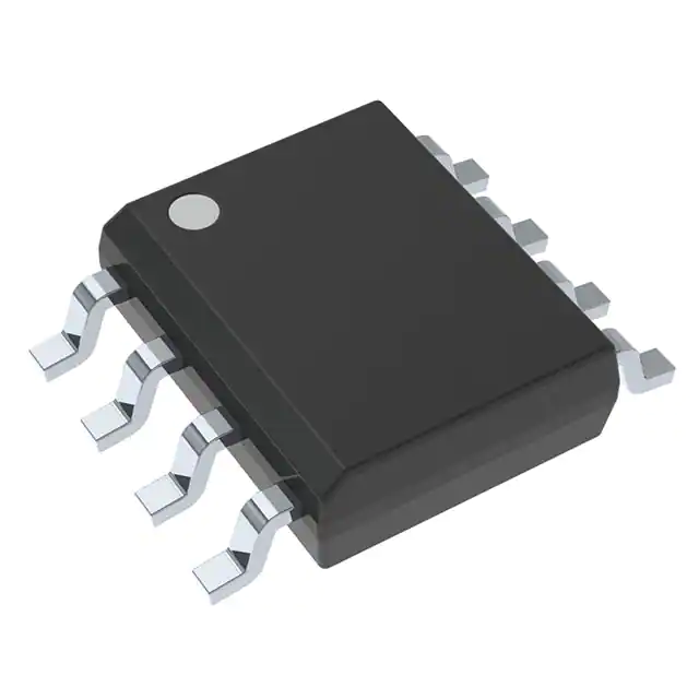
PACKAGE
SOIC (8)
BODY SIZE (NOM)
4.90 mm × 3.91 mm
(1) For all available packages, see the orderable addendum at
the end of the data sheet.
Simplified Schematic
VCC2
Isolation Capacitor
VCC1
SDA1
or SCL1
GND1
SDA2
or SCL2
GND2
VREF
1
An IMPORTANT NOTICE at the end of this data sheet addresses availability, warranty, changes, use in safety-critical applications,
intellectual property matters and other important disclaimers. PRODUCTION DATA.
�ISO1540, ISO1541
SLLSEB6E – JULY 2012 – REVISED APRIL 2019
www.ti.com
Table of Contents
1
2
3
4
5
6
Features ..................................................................
Applications ...........................................................
Description .............................................................
Revision History.....................................................
Pin Configuration and Functions .........................
Specifications.........................................................
6.1
6.2
6.3
6.4
6.5
6.6
6.7
6.8
6.9
6.10
6.11
6.12
6.13
6.14
7
8
1
1
1
2
4
5
Absolute Maximum Ratings ...................................... 5
ESD Ratings.............................................................. 6
Recommended Operating Conditions....................... 6
Thermal Information .................................................. 6
Power Ratings........................................................... 6
Insulation Specifications............................................ 7
Safety-Related Certifications..................................... 8
Safety Limiting Values .............................................. 8
Electrical Characteristics........................................... 9
Supply Current Characteristics ............................. 10
Timing Requirements ............................................ 10
Switching Characteristics ...................................... 11
Insulation Characteristics Curves ......................... 12
Typical Characteristics .......................................... 13
Parameter Measurement Information ................ 16
Detailed Description ............................................ 18
8.1
8.2
8.3
8.4
8.5
9
Overview .................................................................
Functional Block Diagrams .....................................
Feature Description.................................................
Isolator Functional Principle....................................
Device Functional Modes........................................
18
18
19
19
20
Application and Implementation ........................ 21
9.1 Application Information............................................ 21
9.2 Typical Application .................................................. 23
10 Power Supply Recommendations ..................... 25
11 Layout................................................................... 25
11.1 Layout Guidelines ................................................. 25
11.2 Layout Example .................................................... 26
12 Device and Documentation Support ................. 27
12.1
12.2
12.3
12.4
12.5
12.6
12.7
Documentation Support ........................................
Related Links ........................................................
Receiving Notification of Documentation Updates
Community Resources..........................................
Trademarks ...........................................................
Electrostatic Discharge Caution ............................
Glossary ................................................................
27
27
27
27
27
27
27
13 Mechanical, Packaging, and Orderable
Information ........................................................... 28
4 Revision History
NOTE: Page numbers for previous revisions may differ from page numbers in the current version.
Changes from Revision D (December 2016) to Revision E
Page
•
Changed VDE Standard name From: DIN V VDE V 0884-10 (VDE V 0884-10): 2006-12 To: DIN VDE V 088411:2017-01 in Features ......................................................................................................................................................... 1
•
Changed Features bullet From: CSA Component Acceptance Notice 5A, IEC 60950-1 and IEC 61010-1 End
Equipment Standards To: CSA approval per IEC 60950-1 and IEC 62368-1 end equipment standards.............................. 1
•
Updated certifications approval status, numbers, standard names, and details according to the latest agency
certificates in Safety-Related Certifications table ................................................................................................................... 8
•
Changed both bypass capacitors From: 10 µF To: 0.1 µF in Figure 31. Even though larger capacitors can be used,
0.1 µF is the minimum recommended bypass capacitor size. ............................................................................................. 24
•
Changed both bypass capacitors From: 10 µF To: 0.1 µF in Figure 32. Even though larger capacitors can be used,
0.1 µF is the minimum recommended bypass capacitor size. ............................................................................................. 24
Changes from Revision C (June 2015) to Revision D
Page
•
Deleted the Device Comparison Table; see the Features List table for device comparison ................................................ 4
•
Changed the status of CQC certification from planned to certified ....................................................................................... 8
•
Changed the Regulatory Information table to Safety-Related Certifications and updated content........................................ 8
•
Changed formatting of supply current parameters to combine device and sides. Moved parameters to separate table ... 10
•
Added the Receiving Notification of Documentation Updates section ................................................................................ 27
Changes from Revision B (May 2013) to Revision C
•
2
Page
Added Pin Configuration and Functions section, ESD Ratings table, Feature Description section, Device Functional
Modes, Application and Implementation section, Power Supply Recommendations section, Layout section, Device
and Documentation Support section, and Mechanical, Packaging, and Orderable Information section .............................. 1
Submit Documentation Feedback
Copyright © 2012–2019, Texas Instruments Incorporated
Product Folder Links: ISO1540 ISO1541
�ISO1540, ISO1541
www.ti.com
SLLSEB6E – JULY 2012 – REVISED APRIL 2019
•
VDE Standard changed to DIN V VDE V 0884-10 (VDE V 0884-10): 2006-12 .................................................................... 1
•
Changed minimum air gap (Clearance) parameter, L(I01), to external clearance, CLR, and minimum external
tracking (creepage) parameter, L(I02), to external creepage................................................................................................. 7
•
Changed values and test conditions in the Insulation Specifications table ............................................................................ 7
•
Changed the descriptions of VDE and CSA information ....................................................................................................... 8
Changes from Revision A (October 2012) to Revision B
Page
•
Change Safety Feature From: (VDE 0884 Part 2) (Pending) To: (VDE 0884 Part 2) (Approved)......................................... 1
•
Changed, VDE column From: File number: 40016131 (pending) To: File number: 40016131.............................................. 8
Changes from Original (July 2012) to Revision A
Page
•
Changed From: CSA Component Acceptance Notice 5A (Pending) To: CSA Component Acceptance Notice 5A
(Approved) .............................................................................................................................................................................. 1
•
Changed From: IEC 60950-1 and IEC 61010-1 End Equipment Standards (Pending) To: IEC 60950-1 and IEC
61010-1 End Equipment Standards (Approved)..................................................................................................................... 1
•
Changed Safety-Related Certifications, CSA column From: File number: 220991 (pending) To: File number: 220991....... 8
Submit Documentation Feedback
Copyright © 2012–2019, Texas Instruments Incorporated
Product Folder Links: ISO1540 ISO1541
3
�ISO1540, ISO1541
SLLSEB6E – JULY 2012 – REVISED APRIL 2019
www.ti.com
5 Pin Configuration and Functions
ISO1540 D Package
8-Pin SOIC
Top View
1
8
VCC2
SDA1
2
7
SDA2
SCL1
3
6
SCL2
GND1
4
5
GND2
Isolation
VCC1
Side 1
Side 2
Not to scale
Pin Functions—ISO1540
PIN
NAME
NO.
GND1
4
GND2
SCL1
I/O
DESCRIPTION
—
Ground, side 1
5
—
Ground, side 2
3
I/O
Serial clock input / output, side 1
SCL2
6
I/O
Serial clock input / output, side 2
SDA1
2
I/O
Serial data input / output, side 1
SDA2
7
I/O
Serial data input / output, side 2
VCC1
1
—
Supply voltage, side 1
VCC2
8
—
Supply voltage, side 2
4
Submit Documentation Feedback
Copyright © 2012–2019, Texas Instruments Incorporated
Product Folder Links: ISO1540 ISO1541
�ISO1540, ISO1541
www.ti.com
SLLSEB6E – JULY 2012 – REVISED APRIL 2019
ISO1541 D Package
8-Pin SOIC
Top View
1
8
VCC2
SDA1
2
7
SDA2
SCL1
3
6
SCL2
GND1
4
5
GND2
Isolation
VCC1
Side 1
Side 2
Not to scale
Pin Functions—ISO1541
PIN
I/O
DESCRIPTION
NAME
NO.
GND1
4
—
Ground, side 1
GND2
5
—
Ground, side 2
SCL1
3
I
Serial clock input, side 1
SCL2
6
O
Serial clock output, side 2
SDA1
2
I/O
Serial data input / output, side 1
SDA2
7
I/O
Serial data input / output, side 2
VCC1
1
—
Supply voltage, side 1
VCC2
8
—
Supply voltage, side 2
6 Specifications
6.1 Absolute Maximum Ratings
over operating free-air temperature range (unless otherwise noted) (1) (2)
Voltage
MIN
MAX
VCC1, VCC2
–0.5
6
SDA1, SCL1
–0.5
VCC1 + 0.5 (3)
SDA2, SCL2
–0.5
VCC2 + 0.5 (3)
SDA1, SCL1
–20
20
SDA2, SCL2
–100
100
IO
Output current
TJ(MAX)
Maximum junction temperature
Tstg
Storage temperature
(1)
(2)
(3)
–65
UNIT
V
mA
150
°C
150
°C
Stresses beyond those listed under Absolute Maximum Ratings may cause permanent damage to the device. These are stress ratings
only, which do not imply functional operation of the device at these or any other conditions beyond those indicated under Recommended
Operating Conditions. Exposure to absolute-maximum-rated conditions for extended periods may affect device reliability.
All voltage values here within are with respect to the local ground pin (GND1 or GND2) and are peak voltage values.
Maximum voltage must not exceed 6 V.
Submit Documentation Feedback
Copyright © 2012–2019, Texas Instruments Incorporated
Product Folder Links: ISO1540 ISO1541
5
�ISO1540, ISO1541
SLLSEB6E – JULY 2012 – REVISED APRIL 2019
www.ti.com
6.2 ESD Ratings
VALUE
Human body model (HBM), per ANSI/ESDA/JEDEC
JS-001 (1)
V(ESD)
(1)
(2)
Electrostatic discharge
Bus pins
±8000
All pins
±4000
Charged-device model (CDM), per JEDEC specification JESD22C101 (2)
±1500
Machine Model JEDEC JESD22-A115-A, all pins
±200
UNIT
V
JEDEC document JEP155 states that 500-V HBM allows safe manufacturing with a standard ESD control process.
JEDEC document JEP157 states that 250-V CDM allows safe manufacturing with a standard ESD control process.
6.3 Recommended Operating Conditions
MIN
MAX
VCC1, VCC2
Supply voltage
3
5.5
V
VSDA1, VSCL1
Input and output signal voltages, side 1
0
VCC1
V
VSDA2, VSCL2
Input and output signal voltages, side 2
0
VCC2
V
VIL1
Low-level input voltage, side 1
0
0.5
V
VIH1
High-level input voltage, side 1
0.7 × VCC1
VCC1
V
VIL2
Low-level input voltage, side 2
0
0.3 × VCC2
V
VIH2
High-level input voltage, side 2
0.7 × VCC2
VCC2
IOL1
Output current, side 1
0.5
3.5
mA
IOL2
Output current, side 2
0.5
35
mA
C1
Capacitive load, side 1
40
pF
C2
Capacitive load, side 2
400
pF
(1)
UNIT
V
fMAX
Operating frequency
TA
Ambient temperature
–40
125
°C
TJ
Junction temperature
–40
136
°C
TSD
Thermal shutdown
139
171
°C
(1)
1
MHz
This represents the maximum frequency with the maximum bus load (C) and the maximum current sink (IO). If the system has less bus
capacitance, then higher frequencies can be achieved.
6.4 Thermal Information
ISO154x
THERMAL METRIC (1)
D (SOIC)
UNIT
8 PINS
RθJA
Junction-to-ambient thermal resistance
114.6
°C/W
RθJC(top)
Junction-to-case (top) thermal resistance
69.6
°C/W
RθJB
Junction-to-board thermal resistance
55.3
°C/W
ψJT
Junction-to-top characterization parameter
27.2
°C/W
ψJB
Junction-to-board characterization parameter
54.7
°C/W
RθJC(bot)
Junction-to-case (bottom) thermal resistance
N/A
°C/W
(1)
For more information about traditional and new thermal metrics, see the Semiconductor and IC Package Thermal Metrics application
report (SPRA953).
6.5 Power Ratings
PARAMETER
TEST CONDITIONS
PD
Maximum power dissipation (both sides)
PD1
Maximum power dissipation (side-1)
PD2
Maximum power dissipation (side-2)
6
MIN
VCC1 = VCC2 = 5.5 V, TJ = 150 °C, C1 =
40 pF, C2 = 400 pF;
Input a 1-MHz 50% duty cycle clock signal
Submit Documentation Feedback
TYP
MAX
UNIT
85
mW
34
mW
51
mW
Copyright © 2012–2019, Texas Instruments Incorporated
Product Folder Links: ISO1540 ISO1541
�ISO1540, ISO1541
www.ti.com
SLLSEB6E – JULY 2012 – REVISED APRIL 2019
6.6 Insulation Specifications
PARAMETER
TEST CONDITIONS
VALUE
UNIT
GENERAL
External clearance (1)
Shortest terminal-to-terminal distance through air
>4
mm
CPG
External creepage (1)
Shortest terminal-to-terminal distance across the
package surface
>4
mm
DTI
Distance through the insulation
Minimum internal gap (internal clearance)
0.014
mm
CTI
Comparative tracking index
DIN EN 60112 (VDE 0303-11); IEC 60112
>400
V
Rated mains voltage ≤ 150 VRMS
I–IV
Rated mains voltage ≤ 300 VRMS
I–III
CLR
Material group
II
Overvoltage category
DIN V VDE V 0884-10 (VDE V 0884-10):2006-12
VIORM
VIOTM
Maximum repetitive peak isolation voltage AC voltage (bipolar)
Maximum transient isolation voltage
Apparent charge (3)
qpd
Barrier capacitance, input to output (4)
CIO
Isolation resistance, input to output (4)
RIO
(2)
VTEST = VIOTM
t = 60 s (qualification)
t = 1 s (100% production)
566
VPK
4242
VPK
Method a: After I/O safety test subgroup 2/3, Vini =
VIOTM, tini = 60 s; Vpd(m) = 1.2 × VIORM = 680 VPK, tm
= 10 s
109
Pollution degree
2
Climatic category
40/125/21
Ω
UL 1577
VISO
(1)
(2)
(3)
(4)
Withstand isolation voltage
VTEST = VISO = 2500 VRMS, t = 60 s (qualification);
VTEST = 1.2 × VISO = 3000 VRMS, t = 1 s (100%
production)
2500
VRMS
Creepage and clearance requirements should be applied according to the specific equipment isolation standards of an application. Care
should be taken to maintain the creepage and clearance distance of a board design to ensure that the mounting pads of the isolator on
the printed-circuit board do not reduce this distance. Creepage and clearance on a printed-circuit board become equal in certain cases.
Techniques such as inserting grooves and/or ribs on a printed circuit board are used to help increase these specifications.
This coupler is suitable for basic electrical insulation only within the maximum operating ratings. Compliance with the safety ratings shall
be ensured by means of suitable protective circuits.
Apparent charge is electrical discharge caused by a partial discharge (pd).
All pins on each side of the barrier tied together creating a two-terminal device
Submit Documentation Feedback
Copyright © 2012–2019, Texas Instruments Incorporated
Product Folder Links: ISO1540 ISO1541
7
�ISO1540, ISO1541
SLLSEB6E – JULY 2012 – REVISED APRIL 2019
www.ti.com
6.7 Safety-Related Certifications
VDE
Certified according to DIN VDE V
0884-11:2017-01 and DIN EN
61010-1 (VDE 0411-1):2011-07
CSA
UL
CQC
Certified according to CSA/IEC
60950-1 and CSA/IEC 62368-1
Recognized under UL 1577
Component Recognition
Program
Certified according to GB4943.12011
Basic Insulation
Maximum Transient Overvoltage,
4242 VPK;
Maximum Repetitive Peak Voltage,
566 VPK
2.5-kVRMS Insulation Rating;
400 VRMS Basic Insulation
working voltage per CSA 609501-07+A1+A2 and IEC 60950-1
2nd Ed.+A1+A2;
300 VRMS Basic Insulation
working voltage per CSA 623681-14 and IEC 62368-1:2014,
Single protection, 2500 VRMS
Basic Insulation, Altitude ≤ 5000
m, Tropical Climate, 250 VRMS
maximum working voltage
Certificate number: 40047657
Master contract number: 220991
File number: E181974
Certificate number:
CQC14001109540
6.8 Safety Limiting Values
Safety limiting intends to minimize potential damage to the isolation barrier upon failure of input or output circuitry. A failure of
the I/O can allow low resistance to ground or the supply and, without current limiting, dissipate sufficient power to overheat
the die and damage the isolation barrier, potentially leading to secondary system failures.
PARAMETER
IS
TS
Safety input, output, or supply
current
TEST CONDITIONS
MIN
TYP
MAX
RθJA = 114.6°C/W, VI = 5.5 V, TJ = 150°C, TA = 25°C,
see Figure 1
198
RθJA = 114.6°C/W, VI = 3.6 V, TJ = 150°C, TA = 25°C,
see Figure 1
303
Safety temperature
UNIT
mA
150
°C
The safety-limiting constraint is the maximum junction temperature specified in the data sheet. The power
dissipation and junction-to-air thermal impedance of the device installed in the application hardware determines
the junction temperature. The assumed junction-to-air thermal resistance in the Thermal Information table is that
of a device installed on a high-K test board for leaded surface-mount packages. The power is the recommended
maximum input voltage times the current. The junction temperature is then the ambient temperature plus the
power times the junction-to-air thermal resistance.
8
Submit Documentation Feedback
Copyright © 2012–2019, Texas Instruments Incorporated
Product Folder Links: ISO1540 ISO1541
�ISO1540, ISO1541
www.ti.com
SLLSEB6E – JULY 2012 – REVISED APRIL 2019
6.9 Electrical Characteristics
over recommended operating conditions, unless otherwise noted
PARAMETER
TEST CONDITIONS
MIN
TYP
MAX
UNIT
SIDE 1 (ONLY)
VILT1
Voltage input threshold low, SDA1
and SCL1
500
550
660
mV
VIHT1
Voltage input threshold high, SDA1
and SCL1
540
610
700
mV
VHYST1
Voltage input hysteresis
VIHT1 –VILT1
40
60
VOL1
Low-level output voltage, SDA1
and SCL1 (1)
0.5 mA ≤ (ISDA1 and ISCL1) ≤ 3.5 mA
650
ΔVOIT1
Low-level output voltage to highlevel input voltage threshold
difference, SDA1 and SCL1 (1) (2)
0.5 mA ≤ (ISDA1 and ISCL1) ≤ 3.5 mA
50
mV
800
mV
mV
SIDE 2 (ONLY)
VILT2
Voltage input threshold low, SDA2
and SCL2
0.3 × VCC2
0.4 × VCC2
V
VIHT2
Voltage input threshold high, SDA2
and SCL2
0.4 × VCC2
0.5 × VCC2
V
VHYST2
Voltage input hysteresis
VIHT2 – VILT2
VOL2
Low-level output voltage, SDA2
and SCL2
0.5 mA ≤ (ISDA2 and ISCL2) ≤ 35 mA
0.05 × VCC2
V
0.4
V
10
µA
BOTH SIDES
|II|
Input leakage currents, SDA1,
SCL1, SDA2, and SCL2
VSDA1, VSCL1 = VCC1;
VSDA2, VSCL2 = VCC2
CI
Input capacitance to local ground,
SDA1, SCL1, SDA2, and SCL2
VI = 0.4 × sin(2E6πt) + 2.5 V
CMTI
Common-mode transient immunity
See Figure 21
VCCUV
VCC undervoltage lockout
threshold (3)
(1)
(2)
(3)
0.01
7
pF
25
50
kV/µs
2.1
2.5
2.8
V
This parameter does not apply to the ISO1541 SCL1 line as it is unidirectional.
∆VOIT1 = VOL1 – VIHT1. This represents the minimum difference between a Low-Level Output Voltage and a High-Level Input Voltage
Threshold to prevent a permanent latch condition that would otherwise exist with bidirectional communication.
Any VCC voltages, on either side, less than the minimum will ensure device lockout. Both VCC voltages greater than the maximum will
prevent device lockout.
Submit Documentation Feedback
Copyright © 2012–2019, Texas Instruments Incorporated
Product Folder Links: ISO1540 ISO1541
9
�ISO1540, ISO1541
SLLSEB6E – JULY 2012 – REVISED APRIL 2019
www.ti.com
6.10 Supply Current Characteristics
over recommended operating conditions, unless otherwise noted. For more information, see Figure 19.
PARAMETER
TEST CONDITIONS
MIN
TYP
MAX
VSDA1, VSCL1 = GND1; VSDA2, VSCL2 = GND2;
R1, R2 = Open; C1, C2 = Open
2.4
3.6
VSDA1, VSCL1 = VCC1; VSDA2, VSCL2 = VCC2;
R1, R2 = Open; C1, C2 = Open
2.5
3.8
VSDA1, VSCL1 = GND1; VSDA2, VSCL2 = GND2;
R1, R2 = Open; C1, C2 = Open
2.1
3.3
VSDA1, VSCL1 = VCC1; VSDA2, VSCL2 = VCC2;
R1, R2 = Open; C1, C2 = Open
2.3
3.6
VSDA1, VSCL1 = GND1; VSDA2, VSCL2 = GND2;
R1, R2 = Open; C1, C2 = Open
1.7
2.7
VSDA1, VSCL1 = VCC1; VSDA2, VSCL2 = VCC2;
R1, R2 = Open; C1, C2 = Open
1.9
3.1
VSDA1, VSCL1 = GND1; VSDA2, VSCL2 = GND2;
R1,R2 = Open; C1,C2 = Open
3.1
4.7
VSDA1, VSCL1 = VCC1; VSDA2, VSCL2 = VCC2;
R1, R2 = Open; C1, C2 = Open
3.1
4.7
VSDA1, VSCL1 = GND1; VSDA2, VSCL2 = GND2;
R1, R2 = Open; C1, C2 = Open
2.8
4.4
VSDA1, VSCL1 = VCC1; VSDA2, VSCL2 = VCC2;
R1, R2 = Open; C1, C2 = Open
2.9
4.5
VSDA1, VSCL1 = GND1; VSDA2, VSCL2 = GND2;
R1, R2 = Open; C1, C2 = Open
2.3
3.7
VSDA1, VSCL1 = VCC1; VSDA2, VSCL2 = VCC2;
R1, R2 = Open; C1, C2 = Open
2.5
4
UNIT
3 V ≤ VCC1, VCC2 ≤ 3.6 V
ISO1540
ICC1
Supply current, side 1
ISO1541
ICC2
Supply current, side 2
ISO1540 and
ISO1541
mA
mA
4.5 V ≤ VCC1, VCC2 ≤ 5.5 V
ISO1540
ICC1
Supply current, side 1
ISO1541
ICC2
Supply current, side 2
ISO1540 and
ISO1541
mA
mA
6.11 Timing Requirements
tSP
Input noise filter
tUVLO
Time to recover from UVLO
10
2.7 V to 0.9 V; See Figure 22
Submit Documentation Feedback
MIN
NOM
5
12
30
50
MAX
UNIT
110
µs
ns
Copyright © 2012–2019, Texas Instruments Incorporated
Product Folder Links: ISO1540 ISO1541
�ISO1540, ISO1541
www.ti.com
SLLSEB6E – JULY 2012 – REVISED APRIL 2019
6.12 Switching Characteristics
over recommended operating conditions, unless otherwise noted
PARAMETER
TEST CONDITIONS
MIN
TYP MAX
UNIT
3 V ≤ VCC1, VCC2 ≤ 3.6 V
Output Signal Fall Time
(SDA1, SCL1)
See Figure 19
R1 = 953 Ω,
C1 = 40 pF
0.7 × VCC1 to 0.3 × VCC1
tf1
tf2
Output Signal Fall Time
(SDA2, SCL2)
See Figure 19
R2 = 95.3 Ω,
C2 = 400 pF
tpLH1-2
Low-to-High Propagation
Delay, Side 1 to Side 2
tPHL1-2
High-to-Low Propagation
Delay, Side 1 to Side 2
PWD1-2
Pulse Width Distortion
|tpHL1-2 – tpLH1-2|
tPLH2-1 (1)
Low-to-High Propagation
Delay, Side 2 to Side 1
tPHL2-1 (1)
High-to-Low Propagation
Delay, Side 2 to Side 1
PWD2-1 (1)
Pulse Width Distortion
|tpHL2-1 – tpLH2-1|
tLOOP1 (1)
Round-trip propagation
delay on Side 1
See Figure 19
R1 = 953 Ω,
R2 = 95.3 Ω,
C1, C2 = 10 pF
See Figure 20;
R1 = 953 Ω, C1 = 40 pF
R2 = 95.3 Ω, C2 = 400 pF
8
17
29
0.9 × VCC1 to 900 mV
16
29
48
0.7 × VCC2 to 0.3 × VCC2
14
23
47
0.9 × VCC2 to 400 mV
35
50
100
0.55 V to 0.7 × VCC2
33
65
ns
0.7 V to 0.4 V
90
181
ns
55
123
ns
0.4 × VCC2 to 0.7 × VCC1
47
68
ns
0.4 × VCC2 to 0.9 V
67
109
ns
20
49
ns
100
165
ns
6
11
20
0.4 V to 0.3 × VCC1
ns
ns
4.5 V ≤ VCC1, VCC2 ≤ 5.5 V
Output Signal Fall Time
(SDA1, SCL1)
See Figure 19
R1 = 1430 Ω,
C1 = 40 pF
0.7 × VCC1 to 0.3 × VCC1
tf1
0.9 × VCC1 to 900 mV
13
21
39
Output Signal Fall Time
(SDA2, SCL2)
See Figure 19
R2 = 143 Ω,
C2 = 400 pF
0.7 × VCC2 to 0.3 × VCC2
10
18
35
tf2
0.9 × VCC2 to 400 mV
28
41
76
tpLH1-2
Low-to-High Propagation
Delay, Side 1 to Side 2
0.55 V to 0.7 × VCC2
31
62
ns
tPHL1-2
High-to-Low Propagation
Delay, Side 1 to Side 2
0.7 V to 0.4 V
70
139
ns
PWD1-2
Pulse Width Distortion
|tpHL1-2 – tpLH1-2|
38
80
ns
tPLH2-1 (1)
Low-to-high propagation
delay, side 2 to side 1
0.4 × VCC2 to 0.7 × VCC1
55
80
ns
tPHL2-1 (1)
High-to-low propagation
delay, Side 2 to side 1
0.4 × VCC2 to 0.9 V
47
85
ns
PWD2-1 (1)
Pulse Width Distortion
|tpHL2-1 – tpLH2-1|
8
21
ns
tLOOP1 (1)
Round-trip propagation
delay on side 1
110
180
ns
(1)
See Figure 19
R1 = 1430 Ω,
R2 = 143 Ω,
C1,2 = 10 pF
See Figure 20;
R1 = 1430 Ω, C1 = 40 pF
R2 = 143 Ω, C2 = 400 pF
0.4 V to 0.3 × VCC1
ns
ns
This parameter does not apply to the ISO1541 SCL1 line as it is unidirectional.
Submit Documentation Feedback
Copyright © 2012–2019, Texas Instruments Incorporated
Product Folder Links: ISO1540 ISO1541
11
�ISO1540, ISO1541
SLLSEB6E – JULY 2012 – REVISED APRIL 2019
www.ti.com
6.13 Insulation Characteristics Curves
350
VCC1 = VCC2 = 3.6 V
VCC1 = VCC2 = 5.5 V
Safety Limiting Current (mA)
300
250
200
150
100
50
0
0
50
100
150
Ambient Temperature (qC)
200
Figure 1. Thermal Derating Curve for Limiting Current per VDE
12
Submit Documentation Feedback
Copyright © 2012–2019, Texas Instruments Incorporated
Product Folder Links: ISO1540 ISO1541
�ISO1540, ISO1541
www.ti.com
SLLSEB6E – JULY 2012 – REVISED APRIL 2019
6.14 Typical Characteristics
3.0
0.800
IOL1 = 3.5 mA
IOL1 = 0.5 mA
2.5
0.760
Output Current, IOL1 (mA)
Output Voltage, VOL1 (V)
0.780
0.740
0.720
0.700
0.680
0.660
0.640
2.0
1.5
1.0
0.5
0.0
0.620
-0.5
0
0.600
−40 −25 −10
5
20 35 50 65 80
Free−Air Temperature (°C)
95
0.4
0.5
0.6
20
20
18
18
16
16
14
14
12
10
8
6
0.8
0.9
R1 = 1430 :
R1 = 2.2 k:
12
10
8
6
4
R1= 953 :
R1= 2.2 k:
2
-25
-10
VCC1 = 3.3 V
5
20 35 50 65 80
Free-Air Temperature (qC)
95
2
0
-40
110 125
-25
-10
5
D001
C1 = 40 pF
Fall time measured from 70% to 30% VCC1
VCC1 = 5 V
Figure 4. Side 1: Output Fall Time vs Free-Air Temperature
25
25
Fall Time tf2 (ns)
30
20
15
10
5
20 35 50 65 80
Free-Air Temperature (qC)
95
110 125
D002
C1 = 40 pF
Fall time measured from 70% to 30% VCC1
Figure 5. Side 1: Output Fall Time vs Free-air Temperature
30
20
15
10
5
R2 = 95.3 :
R2 = 2.2 k:
0
-40
0.7
Figure 3. Side 1: Output Low Current vs SDA1 or SCL1
Applied Voltage
Fall Time, tf1 (ns)
Fall Time, tf1 (ns)
0.3
TA = 25°C
4
Fall Time tf2 (ns)
0.2
Applied Voltage, VSDA1, VSCL1 (V)
Figure 2. Side 1: Output Low Voltage vs Free-Air
Temperature
0
-40
0.1
110 125
-25
-10
VCC2 = 3.3 V
5
20 35 50 65 80
Free-Air Temperature (qC)
95
R2 = 143 :
R2 = 2.2 k:
110 125
0
-40
-25
-10
D003
C2 = 400 pF
Fall time measured from 70% to 30% VCC2
Figure 6. Side 2: Output Fall Time vs Free-Air Temperature
VCC2 = 5 V
5
20 35 50 65 80
Free-Air Temperature (qC)
95
110 125
D004
C2 = 400 pF
Fall time measured from 70% to 30% VCC2
Figure 7. Side 2: Output Fall Time vs Free-Air Temperature
Submit Documentation Feedback
Copyright © 2012–2019, Texas Instruments Incorporated
Product Folder Links: ISO1540 ISO1541
13
�ISO1540, ISO1541
SLLSEB6E – JULY 2012 – REVISED APRIL 2019
www.ti.com
Typical Characteristics (continued)
120
45
100
Propagation Delay, tPHL1-2 (ns)
Propagation Delay, t PLH1-2 (ns)
40
35
30
25
20
15
10
80
60
40
20
VCC1 and VCC2 = 3.3 V, R2 = 95.3 :
VCC1 and VCC2 = 5 V, R2 = 143 :
VCC1 and VCC2 = 3.3 V, R2 = 95.3 :
VCC1 and VCC2 = 5 V, R2 = 143 :
5
0
-40
-25
-10
5
20 35 50 65 80
Free-Air Temperature (qC)
95
0
-40
110 125
C2 = 10 pF
20 35 50 65 80
Free-Air Temperature (qC)
95
110 125
D006
90
VCC1 and VCC2 = 3.3 V
VCC1 and VCC2 = 5 V
1045
80
Propagation Delay, t PHL1-2 (ns)
Propagation Delay, tPLH1-2 (ns)
5
Figure 9. tPHL1-2 Propagation Delay vs Free-Air Temperature
1050
1040
1035
1030
1025
1020
1015
1010
70
60
50
40
30
20
VCC1 and VCC2 = 3.3 V
VCC1 and VCC2 = 5 V
10
1005
1000
-40
-25
-10
5
R2 = 2.2 kΩ
20 35 50 65 80
Free-Air Temperature (qC)
95
0
-40
110 125
C2 = 400 pF
70
Propagation Delay, t PHL2-1 (ns)
60
50
40
30
20
-10
5
20 35 50 65 80
Free-Air Temperature (qC)
95
110 125
95
110 125
D008
60
50
40
30
20
VCC1 and VCC2 = 3.3 V, R1 = 953 :
VCC1 and VCC2 = 5 V, R1 = 1430 :
0
-40
-25
-10
D009
C1 = 10 pF
20 35 50 65 80
Free-Air Temperature (qC)
C2 = 400 pF
10
VCC1 and VCC2 = 3.3 V, R1 = 953 :
VCC1 and VCC2 = 5 V, R1 = 1430 :
-25
5
Figure 11. tPHL1-2 Propagation Delay vs Free-Air
Temperature
80
0
-40
-10
R2 = 2.2 kΩ
70
10
-25
D007
Figure 10. tPLH1-2 Propagation Delay vs Free-Air
Temperature
Propagation Delay, t PHL2-1 (ns)
-10
C2 = 10 pF
Figure 8. tPLH1-2 Propagation Delay vs Free-Air Temperature
5
20 35 50 65 80
Free-Air Temperature (qC)
95
110 125
D010
C1 = 10 pF
Figure 12. tPLH2-1 Propagation Delay vs Free-Air
Temperature
14
-25
D005
Figure 13. tPHL2-1 Propagation Delay vs Free-Air
Temperature
Submit Documentation Feedback
Copyright © 2012–2019, Texas Instruments Incorporated
Product Folder Links: ISO1540 ISO1541
�ISO1540, ISO1541
www.ti.com
SLLSEB6E – JULY 2012 – REVISED APRIL 2019
148
80
146
70
Propagation Delay, t PHL2-1 (ns)
Propagation Delay, tPLH2-1 (ns)
Typical Characteristics (continued)
144
142
140
138
136
134
VCC1 and VCC2 = 3.3 V
VCC1 and VCC2 = 5 V
132
-40
-25
-10
5
R1 = 2.2 kΩ
20 35 50 65 80
Free-Air Temperature (qC)
95
60
50
40
30
20
VCC1 and VCC2 = 3.3 V
VCC1 and VCC2 = 5 V
10
0
−40 −25 −10
110 125
D011
C1 = 40 pF
R1 = 2.2 kΩ
Figure 14. tPLH2-1 Propagation Delay vs Free-Air
Temperature
5
20 35 50 65 80
Free-Air Temperature (°C)
C1 = 40 pF
95
110 125
Figure 15. tPHL2-1 Propagation Delay vs Free-Air
Temperature
600
140
120
595
tLOOP1 (ns)
tLOOP1 (ns)
100
80
60
590
585
40
580
20
VCC1 and VCC2 = 3.3 V
VCC1 and VCC2 = 5 V
VCC1 and VCC2 = 3.3 V, R1 = 953 :, R2 = 95.3 :
VCC1 and VCC2 = 5 V, R1 = 1430 :, R2 = 143 :
0
-40
-25
-10
C1 = 40 pF
5
20 35 50 65 80
Free-Air Temperature (qC)
95
110 125
575
-40
-25
C2 = 400 pF
5
20 35 50 65 80
Free-Air Temperature (qC)
C1 = 40 pF
R1 = 2.2 kΩ
Figure 16. tLOOP1 vs Free-Air Temperature
Common-Mode Transient Immunity (kV/Ps)
-10
D013
95
110 125
D014
C2 = 400 pF
R2 = 2.2 kΩ
Figure 17. tLOOP1 vs Free-Air Temperature
70
60
50
40
30
20
10
0
-40
VCC1 and VCC2 = 3.3 V
VCC1 and VCC2 = 5 V
-25
-10
5
20 35 50 65 80
Free-Air Temperature (qC)
95
110 125
D015
Figure 18. CMTI vs Free-Air Temperature
Submit Documentation Feedback
Copyright © 2012–2019, Texas Instruments Incorporated
Product Folder Links: ISO1540 ISO1541
15
�ISO1540, ISO1541
SLLSEB6E – JULY 2012 – REVISED APRIL 2019
www.ti.com
7 Parameter Measurement Information
VCC1
R1
±
+
±
+
R1
VCC2
R2
SDA1
R2
SDA2
ISO1540
ISO1541
SCL2
SCL1
C1
C1
C2
C2
Copyright © 2016, Texas Instruments Incorporated
Figure 19. Test Diagram
VCC2
VCC1
SDA1 or
SCL1
Output
R1
Isolation
VCC1
GND1
C1
tLOOP1
0.3 VCC1
SDA1
SCL1 (ISO1540 Only)
0.4 V
GND1
Copyright © 2016, Texas Instruments Incorporated
Figure 20. tLoop1 Setup and Timing Diagram
VCCx
VCCy
2k
2k
Input
Isolation
+
Output
±
GNDx
GNDy
VCMTI
Figure 21. Common-Mode Transient Immunity Test Circuit
16
Submit Documentation Feedback
Copyright © 2012–2019, Texas Instruments Incorporated
Product Folder Links: ISO1540 ISO1541
�ISO1540, ISO1541
www.ti.com
SLLSEB6E – JULY 2012 – REVISED APRIL 2019
Parameter Measurement Information (continued)
VCCy
VCCx
VCCx
Ry
SDAx or
SCLx
I solatio n
0V
Side x, Side y VCCx,VCCy
Ry
1, 2
3.3 V, 3.3 V 95.3 Ω
2, 1
3.3 V, 3.3 V 953 Ω
+
Output
GNDy
GNDx
or
VCCx
VCCy
VCCy
Ry
SDAx or
SCLx
Isola tion
0V
+
Output
GNDx
GNDy
VCCx or
VCCy
2 .7 V
t
UVLO
0 .9 V
Output
Figure 22. tUVLO Test Circuit and Timing Diagrams
Submit Documentation Feedback
Copyright © 2012–2019, Texas Instruments Incorporated
Product Folder Links: ISO1540 ISO1541
17
�ISO1540, ISO1541
SLLSEB6E – JULY 2012 – REVISED APRIL 2019
www.ti.com
8 Detailed Description
8.1 Overview
The I2C bus is used in a wide range of applications because it is simple to use. The bus consists of a two-wire
communication bus that supports bidirectional data transfer between a master device and several slave devices.
The master, or processor, controls the bus, specifically the serial clock (SCL) line. Data is transferred between
the master and slave through a serial data (SDA) line. This data can be transferred in four speeds: standard
mode (0 to 100 kbps), fast mode (0 to 400 kbps), fast-mode plus (0 to 1 Mbps), and high-speed mode (0 to 3.4
Mbps). The most common speeds are the standard and fast modes.
The I2C bus operates in bidirectional, half-duplex mode, while standard digital isolators are unidirectional devices.
To make efficient use of one technology supporting the other, external circuitry is required that separates the
bidirectional bus into two unidirectional signal paths without introducing significant propagation delay. These
devices have their logic input and output buffers separated by TI's capacitive isolation technology using a silicon
dioxide (SiO2) barrier. When used in conjunction with isolated power supplies, these devices block high voltages,
isolate grounds, and prevent noise currents from entering the local ground and interfering with or damaging
sensitive circuitry.
8.2 Functional Block Diagrams
VCC1
VCC2
SDA2
VREF
Isolation Capacitor
SDA1
SCL1
SCL2
GND1
GND2
VREF
Figure 23. ISO1540 Block Diagram
18
Submit Documentation Feedback
Copyright © 2012–2019, Texas Instruments Incorporated
Product Folder Links: ISO1540 ISO1541
�ISO1540, ISO1541
www.ti.com
SLLSEB6E – JULY 2012 – REVISED APRIL 2019
Functional Block Diagrams (continued)
VCC2
SDA1
SDA2
Isolation Capacitor
VCC1
VREF
SCL1
SCL2
GND1
GND2
Figure 24. ISO1541 Block Diagram
8.3 Feature Description
The device enables a complete isolated I2C interface to be implemented within a small form factor having the
features listed in Table 1.
Table 1. Features List
(1)
PART NUMBER
CHANNEL DIRECTION
ISO1540
Bidirectional (SCL)
Bidirectional (SDA)
ISO1541
Unidirectional (SCL)
Bidirectional (SDA)
RATED ISOLATION (1)
MAXIMUM FREQUENCY
2500 VRMS
4242 VPK
1 MHz
See Safety-Related Certifications for detailed Isolation specifications.
8.4 Isolator Functional Principle
To isolate a bidirectional signal path (SDA or SCL), the ISO1540 internally splits a bidirectional line into two
unidirectional signal lines, each of which is isolated through a single-channel digital isolator. Each channel output
is made open-drain to comply with the open-drain technology of I2C. Side 1 of the ISO1540 connects to a lowcapacitance I2C node, while side 2 is designed for connecting to a fully loaded I2C bus with up to 400 pF of
capacitance.
VCC1
VCC2
A
RPU1
B
SDA1
ISO1540
VC-out
RPU2
SDA2
40 mV
Cnode
50 mV
Cbus
C
D
GND1
VREF
VSDA1
VILT1
VIHT1
VOL1
GND2
Figure 25. SDA Channel Design and Voltage Levels at SDA1
Submit Documentation Feedback
Copyright © 2012–2019, Texas Instruments Incorporated
Product Folder Links: ISO1540 ISO1541
19
�ISO1540, ISO1541
SLLSEB6E – JULY 2012 – REVISED APRIL 2019
www.ti.com
Isolator Functional Principle (continued)
At first sight, the arrangement of the internal buffers suggests a closed signal loop that is prone to latch-up.
However, this loop is broken by implementing an output buffer (B) whose output low-level is raised by a diode
drop to approximately 0.75 V, and the input buffer (C) that consists of a comparator with defined hysteresis. The
comparator’s upper and lower input thresholds then distinguish between the proper low-potential of 0.4 V
(maximum) driven directly by SDA1 and the buffered output low-level of B.
Figure 26 demonstrate the switching behavior of the I2C isolator, ISO1540, between a master node at SDA1 and
a heavy loaded bus at SDA2.
VCC2
VOL1
SDA1
50%
SDA2
VIHT1
30%
Receive
Delay
Receive
Delay
VCC1
Receive
Delay
Transmit
Delay
VCC1
VCC2
VCC2
SDA2
50%
SDA1
VCC1
VCC1
VCC2
Transmit
Delay
VIHT2
30%
Figure 26. SDA Channel Timing in Receive and Transmit Directions
8.4.1 Receive Direction (Left Diagram of Figure 26)
When the I2C bus drives SDA2 low, SDA1 follows after a certain delay in the receive path. The output low is the
buffered output of VOL1 = 0.75 V, which is sufficiently low to be detected by Schmitt-trigger inputs with a minimum
input-low voltage of VIL = 0.9 V at 3 V supply levels.
When SDA2 is released, its voltage potential increases towards VCC2 following the time-constant formed by
RPU2 and Cbus. After the receive delay, SDA1 is released and also rises towards VCC1, following the timeconstant RPU1 × Cnode. Because of the significant lower time-constant, SDA1 may reach VCC1 before SDA2
reaches VCC2 potential.
8.4.2 Transmit Direction (Right Diagram of Figure 26)
When a master drives SDA1 low, SDA2 follows after a certain delay in the transmit direction. When SDA2 turns
low it also causes the output of buffer B to turn low but at a higher 0.75 V level. This level cannot be observed
immediately as it is overwritten by the lower low-level of the master.
However, when the master releases SDA1, the voltage potential increases and first must pass the upper input
threshold of the comparator, VIHT1, to release SDA2. SDA1 then increases further until it reaches the buffered
output level of VOL1 = 0.75 V, maintained by the receive path. When comparator C turns high, SDA2 is released
after the delay in transmit direction. It takes another receive delay until B’s output turns high and fully releases
SDA1 to move toward VCC1 potential.
8.5 Device Functional Modes
Table 2 lists the ISO154x functional modes.
Table 2. Function Table (1)
(1)
(2)
20
POWER STATE
INPUT
OUTPUT
Z
VCC1 or VCC2 < 2.1 V
X
VCC1 and VCC2 > 2.8 V
L
L
VCC1 and VCC2 > 2.8 V
H
Z
VCC1 and VCC2 > 2.8 V
Z (2)
?
H = High Level; L = Low Level; Z = High Impedance or Float; X = Irrelevant; ? = Indeterminate
Invalid input condition as an I2C system requires that a pullup resistor to VCC is connected.
Submit Documentation Feedback
Copyright © 2012–2019, Texas Instruments Incorporated
Product Folder Links: ISO1540 ISO1541
�ISO1540, ISO1541
www.ti.com
SLLSEB6E – JULY 2012 – REVISED APRIL 2019
9 Application and Implementation
NOTE
Information in the following applications sections is not part of the TI component
specification, and TI does not warrant its accuracy or completeness. TI’s customers are
responsible for determining suitability of components for their purposes. Customers should
validate and test their design implementation to confirm system functionality.
9.1 Application Information
9.1.1 I2C Bus Overview
The inter-integrated circuit (I2C) bus is a single-ended, multi-master, 2-wire bus for efficient inter-IC
communication in half-duplex mode.
I2C uses open-drain technology, requiring two lines, serial data (SDA) and serial clock (SCL), to be connected to
VDD by resistors (see Figure 27). Pulling the line to ground is considered a logic zero while letting the line float is
a logic one. This logic is used as a channel access method. Transitions of logic states must occur while the SCL
pin is low. Transitions while the SCL pin is high indicate START and STOP conditions. Typical supply voltages
are 3.3 V and 5 V, although systems with higher or lower voltages are allowed.
VDD
RPU
RPU
RPU
RPU
RPU
RPU
RPU
RPU
SDA
SCL
SDA
SCL
SDA
GND
C
Master
SCL
SDA
GND
ADC
Slave
SCL
GND
DAC
Slave
SDA
SCL
GND
C
Slave
Figure 27. I2C Bus
I2C communication uses a 7-bit address space with 16 reserved addresses, so a theoretical maximum of 112
nodes can communicate on the same bus. In praxis, however, the number of nodes is limited by the specified,
total bus capacitance of 400 pF, which restricts communication distances to a few meters.
The specified signaling rates for the ISO1540 and ISO1541 devices are 100 kbps (standard mode), 400 kbps
(fast mode), 1 Mbps (fast mode plus).
The bus has two roles for nodes: master and slave. A master node issues the clock and slave addresses, and
also initiates and ends data transactions. A slave node receives the clock and addresses and responds to
requests from the master. Figure 28 shows a typical data transfer between master and slave.
Submit Documentation Feedback
Copyright © 2012–2019, Texas Instruments Incorporated
Product Folder Links: ISO1540 ISO1541
21
�ISO1540, ISO1541
SLLSEB6E – JULY 2012 – REVISED APRIL 2019
www.ti.com
Application Information (continued)
7-bit
ADDRESS
SDA
SCL
R/W
ACK
8
9
1 -7
8-bit
DATA
8-bit
DATA
ACK
1 -8
9
ACK /
NACK
1 -8
9
S
P
START
Condition
STOP
condition
Figure 28. Timing Diagram of a Complete Data Transfer
The master initiates a transaction by creating a START condition, following by the 7-bit address of the slave it
wishes to communicate with. This is followed by a single read and write (R/W) bit, representing whether the
master wishes to write to 0, or to read from 1 the slave. The master then releases the SDA line to allow the slave
to acknowledge the receipt of data.
The slave responds with an acknowledge bit (ACK) by pulling the SDA pin low during the entire high time of the
9th clock pulse on the SCL signal, after which the master continues in either transmit or receive mode (according
to the R/W bit sent), while the slave continues in the complementary mode (receive or transmit, respectively).
The address and the 8-bit data bytes are sent most significant bit (MSB) first. The START bit is indicated by a
high-to-low transition of SDA while SCL is high. The STOP condition is created by a low-to-high transition of SDA
while SCL is high.
If the master writes to a slave, it repeatedly sends a byte with the slave sending an ACK bit. In this case, the
master is in master-transmit mode and the slave is in slave-receive mode.
If the master reads from a slave, it repeatedly receives a byte from the slave, while acknowledging (ACK) the
receipt of every byte but the last one (see Figure 29). In this situation, the master is in master-receive mode and
the slave is in slave-transmit mode.
The master ends the transmission with a STOP bit, or may send another START bit to maintain bus control for
further transfers.
S Slave Address W A
From Master to Slave
DATA
A
DATA
A P
A = acknowledge
A = not acknowledge
Master Transmitter writing to Slave Receiver
S = Start
From Slave to Master
P = Stop
S Slave Address R A
DATA
A
DATA
Master Receiver reading from Slave Transmitter
A P
R = Read
W = Write
Figure 29. Transmit or Receive Mode Changes During a Data Transfer
When writing to a slave, a master mainly operates in transmit-mode and only changes to receive-mode when
receiving acknowledgment from the slave.
When reading from a slave, the master starts in transmit-mode and then changes to receive-mode after sending
a READ request (R/W bit = 1) to the slave. The slave continues in the complementary mode until the end of a
transaction.
NOTE
The master ends a reading sequence by not acknowledging (NACK) the last byte
received. This procedure resets the slave state machine and allows the master to send
the STOP command.
22
Submit Documentation Feedback
Copyright © 2012–2019, Texas Instruments Incorporated
Product Folder Links: ISO1540 ISO1541
�ISO1540, ISO1541
www.ti.com
SLLSEB6E – JULY 2012 – REVISED APRIL 2019
9.2 Typical Application
In Figure 30, the ultra low-power microcontroller, MSP430G2132, controls the I2C data traffic of configuration
data and conversion results for the analog inputs and outputs. Low-power data converters build the analog
interface to sensors and actuators. The ISO1541 device provides the required isolation between different ground
potentials of the system controller, remote sensor, and actuator circuitry to prevent ground loop currents that
otherwise may falsify the acquired data.
The entire circuit operates from a single 3.3-V supply. A low-power push-pull converter, SN6501, drives a centertapped transformer with an output that is rectified and linearly regulated to provide a stable 5-V supply for the
data converter.
VS
3.3V
0.1 μF
2
Vcc
D2
1:2.2
3
MBR0520L
1
SN6501
GND D1
10 μF 0.1 μF
OUT
5
ON
GND
5VISO
0.1 μF
8
10 μF
LP2981-50
3
1
4,5
IN
9
2
10
1Ω
10 μF
1
MBR0520L
VDD
SDA
AIN0
4
4 Analog
Inputs
SCL ADS 1115
ADDR
AIN3
GND RDY
3
7
2
SCL
5VISO
SDA
5VISO
ISO- BARRIER
5VISO
0.1 μF
6
22 μF
VOUT
VIN 2
1 μF
REF5040
4
GND
0.1 μF
0.1 μF
1.5 kΩ
1.5 kΩ
2
5
6
1
VCC1
DVcc
XOUT
XIN
MSP430
SDA
G2132
SCL
9
8
DVss
2
1.5 kΩ
8
VCC2
7
SDA2
ISO1541
3
6
SCL1
SCL2
SDA1
GND1
4
0.1 μF
1.5 kΩ
4
GND2
5
3
15 4 12
A2 VDD IOVDD VREFH
1
SDA
VOUTA
10
SCL
DAC8574
9
LDAC
14
VOUTD
A1
8
A0 A3 GND VREFL
11
13 16
6
4 Analog
Outputs
5
Copyright © 2016, Texas Instruments Incorporated
Figure 30. Isolated I2C Data Acquisition System
9.2.1 Design Requirements
The recommended power supply voltages (VCC1 and VCC2) must be from 3 V to 5.5 V. A recommended
decoupling capacitor with a value of 0.1 µF is required between both the VCC1 and GND1 pins, and the VCC2
and GND2 pins to support of power supply voltages transient and to ensure reliable operation at all data rates.
9.2.2 Detailed Design Procedure
The power-supply capacitor with a value of 0.1-µF must be placed as close to the power supply pins as possible.
The recommended placement of the capacitors must be 2-mm maximum from input and output power supply
pins (VCC1 and VCC2).
The maximum load permissible on the input lines, SDA1 and SCL1, is ≤ 40 pF and on the output lines, SDA2
and SCL2, is ≤ 400 pF.
Submit Documentation Feedback
Copyright © 2012–2019, Texas Instruments Incorporated
Product Folder Links: ISO1540 ISO1541
23
�ISO1540, ISO1541
SLLSEB6E – JULY 2012 – REVISED APRIL 2019
www.ti.com
Typical Application (continued)
The minimum pullup resistors on the input lines, SDA1 and SCL1 to VCC1 must be selected in such a way that
input current drawn is ≤ 3.5 mA. The minimum pullup resistors on the input lines, SDA2 and SCL2, to VCC2 must
be selected in such a way that output current drawn is ≤ 35 mA. The maximum pullup resistors on the input lines
(SDA1 and SCL1) to VCC1 and on output lines (SDA1 and SCL1) to VCC2, depends on the load and rise time
requirements on the respective lines.
ISO154 0
2mm
maximu m
2 mm
maximu m
VCC1
1k
SDA1
0.1 F
Isol atio n Capa citor
1k
VCC2
8
1
0.1 F
2
SCL1
3
1k
SDA2
7
SCL2
6
GND1
4
GND2
5
Side 1
1k
Side 2
Figure 31. Typical ISO1540 Circuit Hookup
ISO154 1
2mm
maximu m
2 mm
maximu m
VCC1
VCC2
1k
SDA1
0.1 F
Isol atio n Capa citor
1k
8
1
0.1 F
2
SCL1
3
1k
1k
SDA2
7
SCL2
6
GND2
GND1
4
5
Side 1
Side 2
Figure 32. Typical ISO1541 Circuit Hookup
9.2.3 Application Curve
24
Submit Documentation Feedback
Copyright © 2012–2019, Texas Instruments Incorporated
Product Folder Links: ISO1540 ISO1541
�ISO1540, ISO1541
www.ti.com
SLLSEB6E – JULY 2012 – REVISED APRIL 2019
Typical Application (continued)
o
500 mV/div
TA = 25 C
VCC1 = 3.6 V
900 mV
VOL1
GND1
Time - 50 ns/div
Figure 33. Side 1: Low-to-High Transition
10 Power Supply Recommendations
To help ensure reliable operation at data rates and supply voltages, TI recommends connecting a 0.1-µF bypass
capacitor at the input and output supply pins (VCC1 and VCC2). The capacitors should be placed as close to the
supply pins as possible. If only a single, primary-side power supply is available in an application, isolated power
can be generated for the secondary-side with the help of a transformer driver such as TI's SN6501 device. For
such applications, detailed power supply design and transformer selection recommendations are available in
SN6501 Transformer Driver for Isolated Power Supplies. (SLLSEA0).
11 Layout
11.1 Layout Guidelines
A minimum of four layers is required to accomplish a low EMI PCB design (see Figure 34). Layer stacking should
be in the following order (top-to-bottom): high-speed signal layer, ground plane, power plane and low-frequency
signal layer.
• Routing the high-speed traces on the top layer avoids the use of vias (and the introduction of their
inductances) and allows for clean interconnects between the isolator and the transmitter and receiver circuits
of the data link.
• Placing a solid ground plane next to the high-speed signal layer establishes controlled impedance for
transmission line interconnects and provides an excellent low-inductance path for the return current flow.
• Placing the power plane next to the ground plane creates additional high-frequency bypass capacitance of
approximately 100 pF/in2.
• Routing the slower speed control signals on the bottom layer allows for greater flexibility as these signal links
usually have margin to tolerate discontinuities such as vias.
If an additional supply voltage plane or signal layer is needed, add a second power or ground plane system to
the stack to keep it symmetrical. This makes the stack mechanically stable and prevents it from warping. Also the
power and ground plane of each power system can be placed closer together, thus increasing the high-frequency
bypass capacitance significantly.
For detailed layout recommendations, see the Digital Isolator Design Guide (SLLA284)
11.1.1 PCB Material
For digital circuit boards operating at less than 150 Mbps, (or rise and fall times greater than 1 ns), and trace
lengths of up to 10 inches, use standard FR-4 UL94V-0 printed circuit board. This PCB is preferred over cheaper
alternatives because of lower dielectric losses at high frequencies, less moisture absorption, greater strength and
stiffness, and the self-extinguishing flammability-characteristics.
Submit Documentation Feedback
Copyright © 2012–2019, Texas Instruments Incorporated
Product Folder Links: ISO1540 ISO1541
25
�ISO1540, ISO1541
SLLSEB6E – JULY 2012 – REVISED APRIL 2019
www.ti.com
11.2 Layout Example
High-speed traces
10 mils
Ground plane
40 mils
Keep this
space free
from planes,
traces, pads,
and vias
FR-4
0r ~ 4.5
Power plane
10 mils
Low-speed traces
Figure 34. Recommended Layer Stack
26
Submit Documentation Feedback
Copyright © 2012–2019, Texas Instruments Incorporated
Product Folder Links: ISO1540 ISO1541
�ISO1540, ISO1541
www.ti.com
SLLSEB6E – JULY 2012 – REVISED APRIL 2019
12 Device and Documentation Support
12.1 Documentation Support
12.1.1 Related Documentation
For related documentation see the following:
• Digital Isolator Design Guide (SLLA284)
• ISO154xEVM Low-Power Bidirectional I2C Isolators Evaluation Module (SLLU166)
• TI Isolation Glossary (SLLA353)
• SN6501 Transformer Driver for Isolated Power Supplies. (SLLSEA0)
12.2 Related Links
The table below lists quick access links. Categories include technical documents, support and community
resources, tools and software, and quick access to sample or buy.
Table 3. Related Links
PARTS
PRODUCT FOLDER
SAMPLE & BUY
TECHNICAL
DOCUMENTS
TOOLS &
SOFTWARE
SUPPORT &
COMMUNITY
ISO1540
Click here
Click here
Click here
Click here
Click here
ISO1541
Click here
Click here
Click here
Click here
Click here
12.3 Receiving Notification of Documentation Updates
To receive notification of documentation updates, navigate to the device product folder on ti.com. In the upper
right corner, click on Alert me to register and receive a weekly digest of any product information that has
changed. For change details, review the revision history included in any revised document.
12.4 Community Resources
The following links connect to TI community resources. Linked contents are provided "AS IS" by the respective
contributors. They do not constitute TI specifications and do not necessarily reflect TI's views; see TI's Terms of
Use.
TI E2E™ Online Community TI's Engineer-to-Engineer (E2E) Community. Created to foster collaboration
among engineers. At e2e.ti.com, you can ask questions, share knowledge, explore ideas and help
solve problems with fellow engineers.
Design Support TI's Design Support Quickly find helpful E2E forums along with design support tools and
contact information for technical support.
12.5 Trademarks
E2E is a trademark of Texas Instruments.
All other trademarks are the property of their respective owners.
12.6 Electrostatic Discharge Caution
This integrated circuit can be damaged by ESD. Texas Instruments recommends that all integrated circuits be handled with
appropriate precautions. Failure to observe proper handling and installation procedures can cause damage.
ESD damage can range from subtle performance degradation to complete device failure. Precision integrated circuits may be more
susceptible to damage because very small parametric changes could cause the device not to meet its published specifications.
12.7 Glossary
SLYZ022 — TI Glossary.
This glossary lists and explains terms, acronyms, and definitions.
Submit Documentation Feedback
Copyright © 2012–2019, Texas Instruments Incorporated
Product Folder Links: ISO1540 ISO1541
27
�ISO1540, ISO1541
SLLSEB6E – JULY 2012 – REVISED APRIL 2019
www.ti.com
13 Mechanical, Packaging, and Orderable Information
The following pages include mechanical, packaging, and orderable information. This information is the most
current data available for the designated devices. This data is subject to change without notice and revision of
this document. For browser-based versions of this data sheet, refer to the left-hand navigation.
28
Submit Documentation Feedback
Copyright © 2012–2019, Texas Instruments Incorporated
Product Folder Links: ISO1540 ISO1541
�PACKAGE OPTION ADDENDUM
www.ti.com
6-Feb-2020
PACKAGING INFORMATION
Orderable Device
Status
(1)
Package Type Package Pins Package
Drawing
Qty
Eco Plan
Lead/Ball Finish
MSL Peak Temp
(2)
(6)
(3)
Op Temp (°C)
Device Marking
(4/5)
ISO1540D
ACTIVE
SOIC
D
8
75
Green (RoHS
& no Sb/Br)
NIPDAU
Level-2-260C-1 YEAR
-40 to 125
IS1540
ISO1540DR
ACTIVE
SOIC
D
8
2500
Green (RoHS
& no Sb/Br)
NIPDAU
Level-2-260C-1 YEAR
-40 to 125
IS1540
ISO1541D
ACTIVE
SOIC
D
8
75
Green (RoHS
& no Sb/Br)
NIPDAU
Level-2-260C-1 YEAR
-40 to 125
IS1541
ISO1541DR
ACTIVE
SOIC
D
8
2500
Green (RoHS
& no Sb/Br)
NIPDAU
Level-2-260C-1 YEAR
-40 to 125
IS1541
(1)
The marketing status values are defined as follows:
ACTIVE: Product device recommended for new designs.
LIFEBUY: TI has announced that the device will be discontinued, and a lifetime-buy period is in effect.
NRND: Not recommended for new designs. Device is in production to support existing customers, but TI does not recommend using this part in a new design.
PREVIEW: Device has been announced but is not in production. Samples may or may not be available.
OBSOLETE: TI has discontinued the production of the device.
(2)
RoHS: TI defines "RoHS" to mean semiconductor products that are compliant with the current EU RoHS requirements for all 10 RoHS substances, including the requirement that RoHS substance
do not exceed 0.1% by weight in homogeneous materials. Where designed to be soldered at high temperatures, "RoHS" products are suitable for use in specified lead-free processes. TI may
reference these types of products as "Pb-Free".
RoHS Exempt: TI defines "RoHS Exempt" to mean products that contain lead but are compliant with EU RoHS pursuant to a specific EU RoHS exemption.
Green: TI defines "Green" to mean the content of Chlorine (Cl) and Bromine (Br) based flame retardants meet JS709B low halogen requirements of


 工商网监
湘ICP备2023018690号
工商网监
湘ICP备2023018690号

