Product
Folder
Sample &
Buy
Support &
Community
Tools &
Software
Technical
Documents
LF155, LF156, LF256, LF257
LF355, LF356, LF357
SNOSBH0D – MAY 2000 – REVISED NOVEMBER 2015
LFx5x JFET Input Operational Amplifiers
1 Features
2 Applications
•
•
•
•
•
•
•
•
1
•
•
Advantages
– Replace Expensive Hybrid and Module FET
Op Amps
– Rugged JFETs Allow Blow-Out Free Handling
Compared With MOSFET Input Devices
– Excellent for Low Noise Applications Using
Either High or Low Source Impedance—Very
Low 1/f Corner
– Offset Adjust Does Not Degrade Drift or
Common-Mode Rejection as in Most
Monolithic Amplifiers
– New Output Stage Allows Use of Large
Capacitive Loads (5,000 pF) Without Stability
Problems
– Internal Compensation and Large Differential
Input Voltage Capability
Common Features
– Low Input Bias Current: 30 pA
– Low Input Offset Current: 3 pA
– High Input Impedance: 1012 Ω
– Low Input Noise Current: 0.01 pA/√Hz
– High Common-Mode Rejection Ratio: 100 dB
– Large DC Voltage Gain: 106 dB
Uncommon Features
– Extremely Fast Settling Time to 0.01%:
– 4 μs for the LFx55 devices
– 1.5 μs for the LFx56
– 1.5 μs for the LFx57 (AV = 5)
– Fast Slew Rate:
– 5 V/µs for the LFx55
– 12 V/µs for the LFx56
– 50 V/µs for the LFx57 (AV = 5)
– Wide Gain Bandwidth:
– 2.5 MHz for the LFx55 devices
– 5 MHz for the LFx56
– 20 MHz for the LFx57 (AV = 5)
– Low Input Noise Voltage:
– 20 nV/√Hz for the LFx55
– 12 nV/√Hz for the LFx56
– 12 nV/√Hz for the LFx57 (AV = 5)
Precision High-Speed Integrators
Fast D/A and A/D Converters
High Impedance Buffers
Wideband, Low Noise, Low Drift Amplifiers
Logarithmic Amplifiers
Photocell Amplifiers
Sample and Hold Circuits
3 Description
The LFx5x devices are the first monolithic JFET input
operational amplifiers to incorporate well-matched,
high-voltage JFETs on the same chip with standard
bipolar transistors (BI-FET™ Technology). These
amplifiers feature low input bias and offset
currents/low offset voltage and offset voltage drift,
coupled with offset adjust, which does not degrade
drift or common-mode rejection. The devices are also
designed for high slew rate, wide bandwidth,
extremely fast settling time, low voltage and current
noise and a low 1/f noise corner.
Device Information(1)
PART NUMBER
LFx5x
PACKAGE
BODY SIZE (NOM)
SOIC (8)
4.90 mm × 3.91 mm
TO-CAN (8)
9.08 mm × 9.08 mm
PDIP (8)
9.81 mm × 6.35 mm
(1) For all available packages, see the orderable addendum at
the end of the data sheet.
Simplified Schematic
3 pF in LF357 series
1
An IMPORTANT NOTICE at the end of this data sheet addresses availability, warranty, changes, use in safety-critical applications,
intellectual property matters and other important disclaimers. PRODUCTION DATA.
�LF155, LF156, LF256, LF257
LF355, LF356, LF357
SNOSBH0D – MAY 2000 – REVISED NOVEMBER 2015
www.ti.com
Table of Contents
1
2
3
4
5
6
1
1
1
2
3
4
8
6.1
6.2
6.3
6.4
6.5
4
4
4
5
9 Power Supply Recommendations...................... 33
10 Layout................................................................... 33
5
11 Device and Documentation Support ................. 35
6.6
6.7
6.8
6.9
7
7.2 Functional Block Diagram ....................................... 15
7.3 Feature Description................................................. 16
7.4 Device Functional Modes........................................ 16
Features ..................................................................
Applications ...........................................................
Description .............................................................
Revision History.....................................................
Pin Configuration and Functions .........................
Specifications.........................................................
Absolute Maximum Ratings ......................................
ESD Ratings..............................................................
Recommended Operating Conditions.......................
Thermal Information ..................................................
AC Electrical Characteristics, TA = TJ = 25°C, VS =
±15 V..........................................................................
DC Electrical Characteristics, TA = TJ = 25°C, VS =
±15 V..........................................................................
DC Electrical Characteristics ....................................
Power Dissipation Ratings ........................................
Typical Characteristics ..............................................
Application and Implementation ........................ 17
8.1 Application Information............................................ 17
8.2 Typical Application .................................................. 18
8.3 System Examples ................................................... 20
10.1 Layout Guidelines ................................................. 33
10.2 Layout Example .................................................... 34
11.1
11.2
11.3
11.4
11.5
6
6
7
8
Detailed Description ............................................ 14
7.1 Overview ................................................................. 14
Related Links ........................................................
Community Resources..........................................
Trademarks ...........................................................
Electrostatic Discharge Caution ............................
Glossary ................................................................
35
35
35
35
35
12 Mechanical, Packaging, and Orderable
Information ........................................................... 35
4 Revision History
NOTE: Page numbers for previous revisions may differ from page numbers in the current version.
Changes from Revision C (March 2013) to Revision D
Page
•
Added Pin Configuration and Functions section, ESD Ratings table, Thermal Information table, Feature Description
section, Device Functional Modes, Application and Implementation section, Power Supply Recommendations
section, Layout section, Device and Documentation Support section, and Mechanical, Packaging, and Orderable
Information section ................................................................................................................................................................ 1
•
Removed THIGH parameter as it is redundant to TA maximum ............................................................................................... 4
Changes from Revision B (March 2013) to Revision C
•
2
Page
Changed layout of National Data Sheet to TI format ........................................................................................................... 31
Submit Documentation Feedback
Copyright © 2000–2015, Texas Instruments Incorporated
LF156 LF256 LF356
�LF155, LF156, LF256, LF257
LF355, LF356, LF357
www.ti.com
SNOSBH0D – MAY 2000 – REVISED NOVEMBER 2015
5 Pin Configuration and Functions
LMC Package
8-Pin TO-99
Top View
D or P Package
8-Pin SOIC or PDIP
Top View
Available per JM38510/11401 or
JM38510/11402
Pin Functions
PIN
NAME
NO.
BALANCE
I/O
DESCRIPTION
1, 5
I
Balance for input offset voltage
+INPUT
3
I
Noninverting input
–INPUT
2
I
Inverting input
NC
8
—
No connection
OUTPUT
6
O
Output
V+
7
—
Positive power supply
V–
4
—
Negative power supply
Submit Documentation Feedback
Copyright © 2000–2015, Texas Instruments Incorporated
LF156 LF256 LF356
3
�LF155, LF156, LF256, LF257
LF355, LF356, LF357
SNOSBH0D – MAY 2000 – REVISED NOVEMBER 2015
www.ti.com
6 Specifications
6.1 Absolute Maximum Ratings
over operating free-air temperature range (unless otherwise noted)
(1) (2) (3)
MIN
Supply voltage
Differential input voltage
Input voltage (4)
±22
LF35x
±18
LF15x, LF25x, LF356B
±40
LF35x
±30
LF15x, LF25x, LF356B
±20
LF35x
±16
Output short circuit duration
TJMAX
LF15x
150
LF25x, LF356B, LF35x
115
P package
LF25x, LF356B, LF35x
100
D package
LF25x, LF356B, LF35x
100
TO-99 package
Soldering (10 sec.)
PDIP package
Soldering (10 sec.)
SOIC package
(2)
(3)
(4)
V
V
V
—
°C
300
260
Vapor phase (60 sec.)
LF25x, LF356B, LF35x
Infrared (15 sec.)
LF25x, LF356B, LF35x
°C
215
220
−65
Storage temperature, Tstg
(1)
UNIT
Continuous
LMC package
Soldering
information
(lead temp.)
MAX
LF155x, LF256x, LF356B
150
°C
Stresses beyond those listed under Absolute Maximum Ratings may cause permanent damage to the device. These are stress ratings
only, which do not imply functional operation of the device at these or any other conditions beyond those indicated under Recommended
Operating Conditions. Exposure to absolute-maximum-rated conditions for extended periods may affect device reliability.
The maximum power dissipation for these devices must be derated at elevated temperatures and is dictated by TJMAX, θJA, and the
ambient temperature, TA. The maximum available power dissipation at any temperature is PD = (TJMAX − TA) / θJA or the 25°C PdMAX,
whichever is less.
If Military/Aerospace specified devices are required, contact the TI Sales Office/Distributors for availability and specifications.
Unless otherwise specified the absolute maximum negative input voltage is equal to the negative power supply voltage.
6.2 ESD Ratings
V(ESD)
(1)
(2)
Electrostatic discharge
Human body model (HBM), per ANSI/ESDA/JEDEC JS-001 (1) (2)
VALUE
UNIT
±1000
V
JEDEC document JEP155 states that 500-V HBM allows safe manufacturing with a standard ESD control process.
100 pF discharged through 1.5-kΩ resistor
6.3 Recommended Operating Conditions
over operating free-air temperature range (unless otherwise noted)
Supply voltage, VS
MIN
NOM
MAX
LF15x
±15
VS
±20
LF25x
±15
VS
±20
LF356B
±15
VS
±20
LF35x
TA
4
UNIT
V
±15
LF15x
–55
TA
125
LF25x
–25
TA
85
LF356B
0
TA
70
LF35x
0
TA
70
Submit Documentation Feedback
°C
Copyright © 2000–2015, Texas Instruments Incorporated
LF156 LF256 LF356
�LF155, LF156, LF256, LF257
LF355, LF356, LF357
www.ti.com
SNOSBH0D – MAY 2000 – REVISED NOVEMBER 2015
6.4 Thermal Information
LF155, LF156, LF355, LF357
THERMAL METRIC
(1)
LF356
P (PDIP)
D
(SOIC)
LMC (TO-99)
P (PDIP)
8 PINS
8 PINS
8 PINS
8 PINS
Junction-to-ambient thermal resistance
UNIT
130
195
—
55.2
Still Air
—
—
160
—
400 LF/Min Air Flow
—
—
65
—
RθJC(top)
Junction-to-case (top) thermal resistance
—
—
23
44.5
°C/W
RθJB
Junction-to-board thermal resistance
—
—
—
32.4
°C/W
ψJT
Junction-to-top characterization parameter
—
—
—
21.7
°C/W
ψJB
Junction-to-board characterization parameter
—
—
—
32.3
°C/W
RθJA
(1)
°C/W
For more information about traditional and new thermal metrics, see the Semiconductor and IC Package Thermal Metrics application
report, SPRA953.
6.5 AC Electrical Characteristics, TA = TJ = 25°C, VS = ±15 V
PARAMETER
TEST CONDITIONS
MIN
LFx55
SR
Slew Rate
LF15x: AV = 1
LFx56, LF356B
LFx56, LF356B
LF357: AV = 5
LFx57
LFx55
GBW
ts
Gain Bandwidth
Product
Settling Time to
0.01% (1)
en
MAX
UNIT
5
7.5
12
V/μs
50
2.5
LFx56, LF356B
5
LFx57
20
LFx55
4
LFx56, LF356B
1.5
LFx57
1.5
f = 100 Hz
Equivalent Input
Noise Voltage
TYP
RS = 100 Ω
f = 1000 Hz
LFx55
25
LFx56, LF356B
15
LFx57
15
LFx55
20
LFx56, LF356B
12
LFx57
12
MHz
μs
nV/√Hz
nV/√Hz
LFx55
f = 100 Hz
in
LFx56, LF356B
0.01
pA/√Hz
0.01
pA/√Hz
LFx57
Equivalent Input
Current Noise
LFx55
f = 1000 Hz
LFx56, LF356B
LFx57
LFx55
CIN
Input
Capacitance
LFx56, LF356B
3
pF
LFx57
(1)
Settling time is defined here, for a unity gain inverter connection using 2-kΩ resistors for the LF15x. It is the time required for the error
voltage (the voltage at the inverting input pin on the amplifier) to settle to within 0.01% of its final value from the time a 10-V step input is
applied to the inverter. For the LF357, AV = −5, the feedback resistor from output to input is 2 kΩ and the output step is 10 V (See
Settling Time Test Circuit).
Submit Documentation Feedback
Copyright © 2000–2015, Texas Instruments Incorporated
LF156 LF256 LF356
5
�LF155, LF156, LF256, LF257
LF355, LF356, LF357
SNOSBH0D – MAY 2000 – REVISED NOVEMBER 2015
www.ti.com
6.6 DC Electrical Characteristics, TA = TJ = 25°C, VS = ±15 V
PARAMETER
TEST CONDITIONS
Supply current
TYP
MAX
LF155
MIN
2
4
LF355
2
4
LFx56, LF356B
5
7
LF356
5
10
LF357
5
10
UNIT
mA
6.7 DC Electrical Characteristics
See
(1)
PARAMETER
TEST CONDITIONS
TA = 25°C
VOS
RS = 50 Ω
Input offset voltage
TYP
MAX
LF15x, LF25x, LF356B
MIN
3
5
LF35x
3
10
LF15x
Over
temperature
7
LF25x, LF356B
6.5
LF35x
13
ΔVOS/ΔT
Average TC of input
offset voltage
RS = 50 Ω
LF15x, LF25x, LF356B, LF35x
5
ΔTC/ΔVOS
Change in average TC
with VOS adjust
RS = 50 Ω (2)
LF15x, LF25x, LF356B, LF35x
0.5
TJ = 25°C (1)
IOS
(3)
Input offset current
TJ = 25°C (1)
IB
(3)
Input bias current
RIN
AVOL
VO
(1)
(2)
(3)
6
Input resistance
TJ = 25°C
Large signal voltage gain
VS = ±15 V,
VO = ±10 V,
RL = 2 kΩ
Output voltage swing
3
20
3
50
Over
temperature
pA
20
LF25x, LF356B
1
LF35x
2
LF15x, LF25x, LF356B
30
100
LF35x
30
200
nA
pA
50
LF25x, LF356B
5
LF35x
8
1012
LF15x, LF25x, LF356B, LF35x
TA = 25°C
μV/°C
per mV
LF35x
LF15x
TJ ≤ THIGH
mV
μV/°C
LF15x, LF25x, LF356B
LF15x
TJ ≤ THIGH
UNIT
LF15x, LF25x, LF356B
50
200
LF35x
25
200
LF15x, LF25x, LF356B
25
LF35x
nA
Ω
V/mV
15
VS = ±15 V, RL = 10 kΩ
LF15x, LF25x, LF356B, LF35x
±12
±13
VS = ±15 V, RL= 2 kΩ
LF15x, LF25x, LF356B, LF35x
±10
±12
V
Unless otherwise stated, these test conditions apply:
LF15x
LF25x
LF356B
LF35x
Supply Voltage, VS
±15 V ≤ VS ≤ ±20 V
±15 V ≤ VS ≤ ±20 V
±15 V ≤ VS ≤ ±20 V
VS = ±15 V
TA
−55°C ≤ TA ≤ +125°C
−25°C ≤ TA ≤ +85°C
0°C ≤ TA ≤ +70°C
0°C ≤ TA ≤ +70°C
THIGH
+125°C
+85°C
+70°C
+70°C
and VOS, IB and IOS are measured at VCM = 0.
The Temperature Coefficient of the adjusted input offset voltage changes only a small amount (0.5 μV/°C typically) for each mV of
adjustment from its original unadjusted value. Common-mode rejection and open-loop voltage gain are also unaffected by offset
adjustment.
The input bias currents are junction leakage currents which approximately double for every 10°C increase in the junction temperature,
TJ. Due to limited production test time, the input bias currents measured are correlated to junction temperature. In normal operation the
junction temperature rises above the ambient temperature as a result of internal power dissipation, Pd. TJ = TA + θJA Pd where θJA is
the thermal resistance from junction to ambient. Use of a heat sink is recommended if input bias current is to be kept to a minimum.
Submit Documentation Feedback
Copyright © 2000–2015, Texas Instruments Incorporated
LF156 LF256 LF356
�LF155, LF156, LF256, LF257
LF355, LF356, LF357
www.ti.com
SNOSBH0D – MAY 2000 – REVISED NOVEMBER 2015
DC Electrical Characteristics (continued)
See (1)
PARAMETER
TEST CONDITIONS
VCM, High
Input common-mode
voltage range
VCM
VS = ±15 V
MIN
TYP
LF15x, LF25x, LF356B
11
15.1
LF35x
10
15.1
LF15x, LF25x, LF356B
VCM, Low
LF35x
−12
–11
−12
–10
CMRR
Common-mode rejection
ratio
LF15x, LF25x, LF356B
LF35x
80
100
PSRR
Supply voltage rejection
ratio (4)
LF15x, LF25x, LF356B
85
100
LF35x
80
100
(4)
MAX
85
100
UNIT
V
dB
dB
Supply Voltage Rejection is measured for both supply magnitudes increasing or decreasing simultaneously, in accordance with common
practice.
6.8 Power Dissipation Ratings
MIN
LMC Package (Still Air)
Power Dissipation at
TA = 25°C (1) (2)
(1)
(2)
MAX
LF15x
560
LF25x, LF356B, LF35x
400
LMC Package
(400 LF/Min Air Flow)
LF15x
1200
LF25x, LF356B, LF35x
1000
P Package
LF25x, LF356B, LF35x
670
D Package
LF25x, LF356B, LF35x
380
UNIT
mW
The maximum power dissipation for these devices must be derated at elevated temperatures and is dictated by TJMAX, θJA, and the
ambient temperature, TA. The maximum available power dissipation at any temperature is PD = (TJMAX − TA) / θJA or the 25°C PdMAX,
whichever is less.
Maximum power dissipation is defined by the package characteristics. Operating the part near the maximum power dissipation may
cause the part to operate outside specified limits.
Submit Documentation Feedback
Copyright © 2000–2015, Texas Instruments Incorporated
LF156 LF256 LF356
7
�LF155, LF156, LF256, LF257
LF355, LF356, LF357
SNOSBH0D – MAY 2000 – REVISED NOVEMBER 2015
www.ti.com
6.9 Typical Characteristics
6.9.1 Typical DC Performance Characteristics
Curves are for LF155 and LF156 unless otherwise specified.
8
Figure 1. Input Bias Current
Figure 2. Input Bias Current
Figure 3. Input Bias Current
Figure 4. Voltage Swing
Figure 5. Supply Current
Figure 6. Supply Current
Submit Documentation Feedback
Copyright © 2000–2015, Texas Instruments Incorporated
LF156 LF256 LF356
�LF155, LF156, LF256, LF257
LF355, LF356, LF357
www.ti.com
SNOSBH0D – MAY 2000 – REVISED NOVEMBER 2015
Typical DC Performance Characteristics (continued)
Curves are for LF155 and LF156 unless otherwise specified.
Figure 7. Negative Current Limit
Figure 8. Positive Current Limit
Figure 9. Positive Common-Mode Input Voltage Limit
Figure 10. Negative Common-Mode Input Voltage Limit
Figure 11. Open-Loop Voltage Gain
Figure 12. Output Voltage Swing
Submit Documentation Feedback
Copyright © 2000–2015, Texas Instruments Incorporated
LF156 LF256 LF356
9
�LF155, LF156, LF256, LF257
LF355, LF356, LF357
SNOSBH0D – MAY 2000 – REVISED NOVEMBER 2015
www.ti.com
6.9.2 Typical AC Performance Characteristics
10
Figure 13. Gain Bandwidth
Figure 14. Gain Bandwidth
Figure 15. Normalized Slew Rate
Figure 16. Output Impedance
Figure 17. Output Impedance
Figure 18. LF155 Small Signal Pulse Response, AV = +1
Submit Documentation Feedback
Copyright © 2000–2015, Texas Instruments Incorporated
LF156 LF256 LF356
�LF155, LF156, LF256, LF257
LF355, LF356, LF357
www.ti.com
SNOSBH0D – MAY 2000 – REVISED NOVEMBER 2015
Typical AC Performance Characteristics (continued)
Figure 19. LF156 Small Signal Pulse Response, AV = +1
Figure 20. LF155 Large Signal Pulse Response, AV = +1
Figure 21. LF156 Large Signal Puls Response, AV = +1
Figure 22. Inverter Settling Time
Figure 23. Inverter Settling Time
Figure 24. Open-Loop Frequency Response
Submit Documentation Feedback
Copyright © 2000–2015, Texas Instruments Incorporated
LF156 LF256 LF356
11
�LF155, LF156, LF256, LF257
LF355, LF356, LF357
SNOSBH0D – MAY 2000 – REVISED NOVEMBER 2015
www.ti.com
Typical AC Performance Characteristics (continued)
12
Figure 25. Bode Plot
Figure 26. Bode Plot
Figure 27. Bode Plot
Figure 28. Common-Mode Rejection Ratio
Figure 29. Power Supply Rejection Ratio
Figure 30. Power Supply Rejection Ratio
Submit Documentation Feedback
Copyright © 2000–2015, Texas Instruments Incorporated
LF156 LF256 LF356
�LF155, LF156, LF256, LF257
LF355, LF356, LF357
www.ti.com
SNOSBH0D – MAY 2000 – REVISED NOVEMBER 2015
Typical AC Performance Characteristics (continued)
Figure 31. Undistorted Output Voltage Swing
Figure 32. Equivalent Input Noise Voltage
Figure 33. Equivalent Input Noise Voltage (Expanded Scale)
Submit Documentation Feedback
Copyright © 2000–2015, Texas Instruments Incorporated
LF156 LF256 LF356
13
�LF155, LF156, LF256, LF257
LF355, LF356, LF357
SNOSBH0D – MAY 2000 – REVISED NOVEMBER 2015
www.ti.com
7 Detailed Description
7.1 Overview
These are the first monolithic JFET input operational amplifiers to incorporate well matched, high voltage JFETs
on the same chip with standard bipolar transistors (BI-FET Technology). These amplifiers feature low input bias
and offset currents, as well as low offset voltage and offset voltage drift, coupled with offset adjust which does
not degrade drift or common-mode rejection. These devices can replace expensive hybrid and module FET
operational amplifiers. Designed for low voltage and current noise and a low 1/f noise corner, these devices are
excellent for low noise applications using either high or low source impedance.
14
Submit Documentation Feedback
Copyright © 2000–2015, Texas Instruments Incorporated
LF156 LF256 LF356
�LF155, LF156, LF256, LF257
LF355, LF356, LF357
www.ti.com
SNOSBH0D – MAY 2000 – REVISED NOVEMBER 2015
7.2 Functional Block Diagram
*C = 3 pF in LF357 series.
Figure 34. Detailed Schematic
Submit Documentation Feedback
Copyright © 2000–2015, Texas Instruments Incorporated
LF156 LF256 LF356
15
�LF155, LF156, LF256, LF257
LF355, LF356, LF357
SNOSBH0D – MAY 2000 – REVISED NOVEMBER 2015
www.ti.com
7.3 Feature Description
7.3.1 Large Differential Input Voltage
These are operational amplifiers with JFET input devices. These JFETs have large reverse breakdown voltages
from gate to source and drain eliminating the need for clamps across the inputs. Therefore large differential input
voltages can easily be accommodated without a large increase in input current. The maximum differential input
voltage is independent of the supply voltages. However, neither of the input voltages should be allowed to
exceed the negative supply as this will cause large currents to flow which can result in a destroyed unit.
7.3.2 Large Common-Mode Input Voltage
These amplifiers will operate with the common-mode input voltage equal to the positive supply. In fact, the
common-mode voltage can exceed the positive supply by approximately 100 mV independent of supply voltage
and over the full operating temperature range. The positive supply can therefore be used as a reference on an
input as, for example, in a supply current monitor and/or limiter.
7.4 Device Functional Modes
The LFx5x has a single functional mode and operates according to the conditions listed in the Recommended
Operating Conditions.
16
Submit Documentation Feedback
Copyright © 2000–2015, Texas Instruments Incorporated
LF156 LF256 LF356
�LF155, LF156, LF256, LF257
LF355, LF356, LF357
www.ti.com
SNOSBH0D – MAY 2000 – REVISED NOVEMBER 2015
8 Application and Implementation
NOTE
Information in the following applications sections is not part of the TI component
specification, and TI does not warrant its accuracy or completeness. TI’s customers are
responsible for determining suitability of components for their purposes. Customers should
validate and test their design implementation to confirm system functionality.
8.1 Application Information
These are op amps with JFET input devices. These JFETs have large reverse breakdown voltages from gate to
source and drain eliminating the need for clamps across the inputs. Therefore large differential input voltages can
easily be accommodated without a large increase in input current. The maximum differential input voltage is
independent of the supply voltages. However, neither of the input voltages should be allowed to exceed the
negative supply as this will cause large currents to flow which can result in a destroyed unit.
Exceeding the negative common-mode limit on either input will force the output to a high state, potentially
causing a reversal of phase to the output. Exceeding the negative common-mode limit on both inputs will force
the amplifier output to a high state. In neither case does a latch occur since raising the input back within the
common-mode range again puts the input stage and thus the amplifier in a normal operating mode.
Exceeding the positive common-mode limit on a single input will not change the phase of the output however, if
both inputs exceed the limit, the output of the amplifier will be forced to a high state.
These amplifiers will operate with the common-mode input voltage equal to the positive supply. In fact, the
common-mode voltage can exceed the positive supply by approximately 100 mV independent of supply voltage
and over the full operating temperature range. The positive supply can therefore be used as a reference on an
input as, for example, in a supply current monitor and/or limiter.
Precautions should be taken to ensure that the power supply for the integrated circuit never becomes reversed in
polarity or that the unit is not inadvertently installed backwards in a socket as an unlimited current surge through
the resulting forward diode within the IC could cause fusing of the internal conductors and result in a destroyed
unit.
All of the bias currents in these amplifiers are set by FET current sources. The drain currents for the amplifiers
are therefore essentially independent of supply voltage.
As with most amplifiers, care should be taken with lead dress, component placement and supply decoupling in
order to ensure stability. For example, resistors from the output to an input should be placed with the body close
to the input to minimize pick-up and maximize the frequency of the feedback pole by minimizing the capacitance
from the input to ground.
A feedback pole is created when the feedback around any amplifier is resistive. The parallel resistance and
capacitance from the input of the device (usually the inverting input) to AC ground set the frequency of the pole.
In many instances the frequency of this pole is much greater than the expected 3-dB frequency of the closed
loop gain and consequently there is negligible effect on stability margin. However, if the feedback pole is less
than approximately six times the expected 3-dB frequency a lead capacitor should be placed from the output to
the input of the op amp. The value of the added capacitor should be such that the RC time constant of this
capacitor and the resistance it parallels is greater than or equal to the original feedback pole time constant.
Submit Documentation Feedback
Copyright © 2000–2015, Texas Instruments Incorporated
LF156 LF256 LF356
17
�LF155, LF156, LF256, LF257
LF355, LF356, LF357
SNOSBH0D – MAY 2000 – REVISED NOVEMBER 2015
www.ti.com
8.2 Typical Application
Figure 35. Settling Time Test Circuit
8.2.1 Design Requirements
Settling time is tested with the LF35x connected as unity gain inverter and LF357 connected for AV = −5
8.2.2 Detailed Design Procedure
Connect the circuit components as shown in Figure 35. In particular, use FET to isolate the probe capacitance.
Apply a 10-V step function to the input.
Use an oscilloscope to probe the circuit as shown in Figure 35.
18
Submit Documentation Feedback
Copyright © 2000–2015, Texas Instruments Incorporated
LF156 LF256 LF356
�LF155, LF156, LF256, LF257
LF355, LF356, LF357
www.ti.com
SNOSBH0D – MAY 2000 – REVISED NOVEMBER 2015
Typical Application (continued)
8.2.3 Application Curves
Large Signal Inverter Output, VOUT (from Settling Time Circuit)
Figure 36. LF355
Figure 37. LF356
Figure 38. LF357
Submit Documentation Feedback
Copyright © 2000–2015, Texas Instruments Incorporated
LF156 LF256 LF356
19
�LF155, LF156, LF256, LF257
LF355, LF356, LF357
SNOSBH0D – MAY 2000 – REVISED NOVEMBER 2015
www.ti.com
8.3 System Examples
Figure 39. Low Drift Adjustable Voltage Reference
•
•
•
•
•
20
ΔVOUT / ΔT = ±0.002%/°C
All resistors and potentiometers should be wire-wound
P1: drift adjust
P2: VOUT adjust
Use LF155 for
– Low IB
– Low drift
– Low supply current
Submit Documentation Feedback
Copyright © 2000–2015, Texas Instruments Incorporated
LF156 LF256 LF356
�LF155, LF156, LF256, LF257
LF355, LF356, LF357
www.ti.com
SNOSBH0D – MAY 2000 – REVISED NOVEMBER 2015
System Examples (continued)
Figure 40. Fast Logarithmic Converter
•
•
•
•
•
Dynamic range: 100 μA ≤ Ii ≤ 1 mA (5 decades), |VO| = 1 V/decade
Transient response: 3 μs for ΔIi = 1 decade
C1, C2, R2, R3: added dynamic compensation
VOS adjust the LF156 to minimize quiescent error
RT: Tel Labs type Q81 + 0.3%/°C
(1)
Submit Documentation Feedback
Copyright © 2000–2015, Texas Instruments Incorporated
LF156 LF256 LF356
21
�LF155, LF156, LF256, LF257
LF355, LF356, LF357
SNOSBH0D – MAY 2000 – REVISED NOVEMBER 2015
www.ti.com
System Examples (continued)
Figure 41. Precision Current Monitor
•
•
•
22
VO = 5 R1/R2 (V/mA of IS)
R1, R2, R3: 0.1% resistors
Use LF155 for
– Common-mode range to supply range
– Low IB
– Low VOS
– Low Supply Current
Submit Documentation Feedback
Copyright © 2000–2015, Texas Instruments Incorporated
LF156 LF256 LF356
�LF155, LF156, LF256, LF257
LF355, LF356, LF357
www.ti.com
SNOSBH0D – MAY 2000 – REVISED NOVEMBER 2015
System Examples (continued)
Figure 42. 8-Bit D/A Converter With Symmetrical Offset Binary Operation
•
•
R1, R2 should be matched within ±0.05%
Full-scale response time: 3 μs
Table 1. Bit Illustration of the 8-Bit D/A Converter
EO
B1
B2
B3
B4
B5
B6
B7
B8
COMMENTS
+9.920
1
1
1
1
1
1
1
1
Positive Full-Scale
+0.040
1
0
0
0
0
0
0
0
(+) Zero-Scale
−0.040
0
1
1
1
1
1
1
1
(−) Zero-Scale
−9.920
0
0
0
0
0
0
0
0
Negative Full-Scale
Figure 43. Wide BW Low Noise, Low Drift Amplifier
(2)
Submit Documentation Feedback
Copyright © 2000–2015, Texas Instruments Incorporated
LF156 LF256 LF356
23
�LF155, LF156, LF256, LF257
LF355, LF356, LF357
SNOSBH0D – MAY 2000 – REVISED NOVEMBER 2015
www.ti.com
Parasitic input capacitance C1 ≃ (3 pF for LF155, LF156 and LF357 plus any additional layout capacitance)
interacts with feedback elements and creates undesirable high frequency pole. To compensate add C2 such that:
R2 C2 ≃ R1 C1.
Figure 44. Boosting the LF156 With a Current Amplifier
•
IOUT(MAX) ≃ 150 mA (will drive RL ≥ 100 Ω)
(3)
•
No additional phase shift added by the current amplifier
Figure 45. Decades VCO
24
Submit Documentation Feedback
Copyright © 2000–2015, Texas Instruments Incorporated
LF156 LF256 LF356
�LF155, LF156, LF256, LF257
LF355, LF356, LF357
www.ti.com
SNOSBH0D – MAY 2000 – REVISED NOVEMBER 2015
R1, R4 matched. Linearity 0.1% over 2 decades.
(4)
Figure 46. Isolating Large Capacitive Loads
•
•
•
Overshoot 6%
ts 10 μs
When driving large CL, the VOUT slew rate determined by CL and IOUT(MAX):
(5)
Figure 47. Low Drift Peak Detector
•
•
•
•
By adding D1 and Rf, VD1 = 0 during hold mode. Leakage of D2 provided by feedback path through Rf.
Leakage of circuit is essentially Ib (LF155, LF156) plus capacitor leakage of Cp.
Diode D3 clamps VOUT (A1) to VIN − VD3 to improve speed and to limit reverse bias of D2.
Maximum input frequency should be 100
Use LF155 for
– Low IB
– Low supply current
Figure 55. VOS Adjustment
•
•
•
•
VOS is adjusted with a 25-k potentiometer
The potentiometer wiper is connected to V+
For potentiometers with temperature coefficient of 100 ppm/°C or less the additional drift with adjust
is ≈ 0.5 μV/°C/mV of adjustment
Typical overall drift: 5 μV/°C ±(0.5 μV/°C/mV of adj.)
Submit Documentation Feedback
Copyright © 2000–2015, Texas Instruments Incorporated
LF156 LF256 LF356
31
�LF155, LF156, LF256, LF257
LF355, LF356, LF357
SNOSBH0D – MAY 2000 – REVISED NOVEMBER 2015
www.ti.com
Figure 56. Driving Capacitive Loads
•
•
•
*
LF15x R = 5k, LF357 R = 1.25 k
Due to a unique output stage design, these amplifiers have the ability to drive large capacitive loads and still
maintain stability. CL(MAX) ≃ 0.01 μF.
Overshoot ≤ 20%, Settling time (ts) ≃ 5 μs
Figure 57. LF357 - A Large Power BW Amplifier
For distortion ≤ 1% and a 20 Vp-p VOUT swing, power bandwidth is: 500 kHz.
32
Submit Documentation Feedback
Copyright © 2000–2015, Texas Instruments Incorporated
LF156 LF256 LF356
�LF155, LF156, LF256, LF257
LF355, LF356, LF357
www.ti.com
SNOSBH0D – MAY 2000 – REVISED NOVEMBER 2015
9 Power Supply Recommendations
See the Recommended Operating Conditions for the minimum and maximum values for the supply input voltage
and operating junction temperature.
10 Layout
10.1 Layout Guidelines
10.1.1 Printed-Circuit-Board Layout For High-Impedance Work
It is generally recognized that any circuit which must operate with less than 1000 pA of leakage current requires
special layout of the PCB. When one wishes to take advantage of the low input bias current of the LFx5x,
typically less than 30 pA, it is essential to have an excellent layout. Fortunately, the techniques of obtaining low
leakages are quite simple. First, the user must not ignore the surface leakage of the PCB, even though it may
sometimes appear acceptably low, because under conditions of high humidity or dust or contamination, the
surface leakage will be appreciable.
To minimize the effect of any surface leakage, lay out a ring of foil completely surrounding the inputs of the
LFx5x and the terminals of capacitors, diodes, conductors, resistors, relay terminals, and so forth, connected to
the inputs of the op amp, as in Figure 62. To have a significant effect, guard rings must be placed on both the
top and bottom of the PCB. This PC foil must then be connected to a voltage that is at the same voltage as the
amplifier inputs, because no leakage current can flow between two points at the same potential. For example, a
PCB trace-to-pad resistance of 10 TΩ, which is normally considered a very large resistance, could leak 5 pA if
the trace were a 5-V bus adjacent to the pad of the input. If a guard ring is used and held close to the potential of
the amplifier inputs, it will significantly reduce this leakage current.
Figure 58. Inverting Amplifier
Figure 59. Noninverting Amplifier
Submit Documentation Feedback
Copyright © 2000–2015, Texas Instruments Incorporated
LF156 LF256 LF356
33
�LF155, LF156, LF256, LF257
LF355, LF356, LF357
SNOSBH0D – MAY 2000 – REVISED NOVEMBER 2015
www.ti.com
Layout Guidelines (continued)
Figure 60. Typical Connections Of Guard Rings
The designer should be aware that when it is inappropriate to lay out a PCB for the sake of just a few circuits,
there is another technique which is even better than a guard ring on a PCB: Do not insert the input pin of the
amplifier into the board at all, but bend it up in the air and use only air as an insulator. Air is an excellent
insulator. In this case you may have to forego some of the advantages of PCB construction, but the advantages
are sometimes well worth the effort of using point-to-point up-in-the-air wiring. See Figure 61.
(Input pins are lifted out of PCB and soldered directly to components. All other pins connected to PCB).
Figure 61. Air Wiring
Another potential source of leakage that might be overlooked is the device package. When the LFx5x is
manufactured, the device is always handled with conductive finger cots. This is to assure that salts and skin oils
do not cause leakage paths on the surface of the package. We recommend that these same precautions be
adhered to, during all phases of inspection, test and assembly.
10.2 Layout Example
Figure 62. Examples Of Guard
Ring In PCB Layout
34
Submit Documentation Feedback
Copyright © 2000–2015, Texas Instruments Incorporated
LF156 LF256 LF356
�LF155, LF156, LF256, LF257
LF355, LF356, LF357
www.ti.com
SNOSBH0D – MAY 2000 – REVISED NOVEMBER 2015
11 Device and Documentation Support
11.1 Related Links
The table below lists quick access links. Categories include technical documents, support and community
resources, tools and software, and quick access to sample or buy.
Table 2. Related Links
PARTS
PRODUCT FOLDER
SAMPLE & BUY
TECHNICAL
DOCUMENTS
TOOLS &
SOFTWARE
SUPPORT &
COMMUNITY
LF156
Click here
Click here
Click here
Click here
Click here
LF256
Click here
Click here
Click here
Click here
Click here
LF356
Click here
Click here
Click here
Click here
Click here
11.2 Community Resources
The following links connect to TI community resources. Linked contents are provided "AS IS" by the respective
contributors. They do not constitute TI specifications and do not necessarily reflect TI's views; see TI's Terms of
Use.
TI E2E™ Online Community TI's Engineer-to-Engineer (E2E) Community. Created to foster collaboration
among engineers. At e2e.ti.com, you can ask questions, share knowledge, explore ideas and help
solve problems with fellow engineers.
Design Support TI's Design Support Quickly find helpful E2E forums along with design support tools and
contact information for technical support.
11.3 Trademarks
BI-FET, E2E are trademarks of Texas Instruments.
All other trademarks are the property of their respective owners.
11.4 Electrostatic Discharge Caution
These devices have limited built-in ESD protection. The leads should be shorted together or the device placed in conductive foam
during storage or handling to prevent electrostatic damage to the MOS gates.
11.5 Glossary
SLYZ022 — TI Glossary.
This glossary lists and explains terms, acronyms, and definitions.
12 Mechanical, Packaging, and Orderable Information
The following pages include mechanical, packaging, and orderable information. This information is the most
current data available for the designated devices. This data is subject to change without notice and revision of
this document. For browser-based versions of this data sheet, refer to the left-hand navigation.
Submit Documentation Feedback
Copyright © 2000–2015, Texas Instruments Incorporated
LF156 LF256 LF356
35
�PACKAGE OPTION ADDENDUM
www.ti.com
10-Feb-2020
PACKAGING INFORMATION
Orderable Device
Status
(1)
Package Type Package Pins Package
Drawing
Qty
Eco Plan
Lead/Ball Finish
MSL Peak Temp
(2)
(6)
(3)
Op Temp (°C)
Device Marking
(4/5)
LF156 MD8
ACTIVE
DIESALE
Y
0
204
Green (RoHS
& no Sb/Br)
Call TI
Level-1-NA-UNLIM
-55 to 125
LF156H
ACTIVE
TO-99
LMC
8
500
TBD
Call TI
Call TI
-55 to 125
( LF156H, LF156H)
LF156H/NOPB
ACTIVE
TO-99
LMC
8
500
Green (RoHS
& no Sb/Br)
Call TI
Level-1-NA-UNLIM
-55 to 125
( LF156H, LF156H)
LF256H
ACTIVE
TO-99
LMC
8
500
TBD
Call TI
Call TI
-25 to 85
( LF256H, LF256H)
LF256H/NOPB
ACTIVE
TO-99
LMC
8
500
Green (RoHS
& no Sb/Br)
Call TI
Level-1-NA-UNLIM
-25 to 85
( LF256H, LF256H)
LF356M
NRND
SOIC
D
8
95
TBD
Call TI
Call TI
0 to 70
LF356
M
LF356M/NOPB
ACTIVE
SOIC
D
8
95
Green (RoHS
& no Sb/Br)
SN
Level-1-260C-UNLIM
0 to 70
LF356
M
LF356MX/NOPB
ACTIVE
SOIC
D
8
2500
Green (RoHS
& no Sb/Br)
SN
Level-1-260C-UNLIM
0 to 70
LF356
M
LF356N/NOPB
ACTIVE
PDIP
P
8
40
Green (RoHS
& no Sb/Br)
Call TI | SN
Level-1-NA-UNLIM
0 to 70
LF
356N
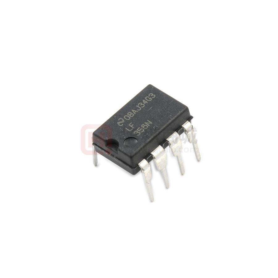
(1)
The marketing status values are defined as follows:
ACTIVE: Product device recommended for new designs.
LIFEBUY: TI has announced that the device will be discontinued, and a lifetime-buy period is in effect.
NRND: Not recommended for new designs. Device is in production to support existing customers, but TI does not recommend using this part in a new design.
PREVIEW: Device has been announced but is not in production. Samples may or may not be available.
OBSOLETE: TI has discontinued the production of the device.
(2)
RoHS: TI defines "RoHS" to mean semiconductor products that are compliant with the current EU RoHS requirements for all 10 RoHS substances, including the requirement that RoHS substance
do not exceed 0.1% by weight in homogeneous materials. Where designed to be soldered at high temperatures, "RoHS" products are suitable for use in specified lead-free processes. TI may
reference these types of products as "Pb-Free".
RoHS Exempt: TI defines "RoHS Exempt" to mean products that contain lead but are compliant with EU RoHS pursuant to a specific EU RoHS exemption.
Green: TI defines "Green" to mean the content of Chlorine (Cl) and Bromine (Br) based flame retardants meet JS709B low halogen requirements of


 工商网监
湘ICP备2023018690号
工商网监
湘ICP备2023018690号

