Product
Folder
Sample &
Buy
Technical
Documents
Support &
Community
Tools &
Software
LF412-N
SNOSBH7F – APRIL 1999 – REVISED SEPTEMBER 2014
LF412-N Low Offset, Low Drift Dual JFET Input Operational Amplifier
1 Features
3 Description
•
•
•
•
•
•
•
•
•
•
•
These devices are low cost, high speed, JFET input
operational amplifiers with very low input offset
voltage and input offset voltage drift. They require low
supply current yet maintain a large gain bandwidth
product and fast slew rate. In addition, well matched
high voltage JFET input devices provide very low
input bias and offset currents. The LF412-N dual is
pin compatible with the LM1558, allowing designers
to immediately upgrade the overall performance of
existing designs.
1
Internally Trimmed Offset Voltage: 1 mV (Max)
Input Offset Voltage Drift: 7 µV/°C (Typ)
Low Input Bias Current: 50 pA
Low Input Noise Current: 0.01 pA / √Hz
Wide Gain Bandwidth: 3 MHz (Min)
High Slew Rate: 10V/µs (Min)
Low Supply Current: 1.8 mA/Amplifier
High Input Impedance: 1012Ω
Low Total Harmonic Distortion: ≤0.02%
Low 1/f Noise Corner: 50 Hz
Fast Settling Time to 0.01%: 2 µs
2 Applications
•
•
•
High Speed Integrators
Fast D/A Converters
Sample and Hold Circuits
These amplifiers may be used in applications such as
high speed integrators, fast D/A converters, sample
and hold circuits and many other circuits requiring low
input offset voltage and drift, low input bias current,
high input impedance, high slew rate and wide
bandwidth.
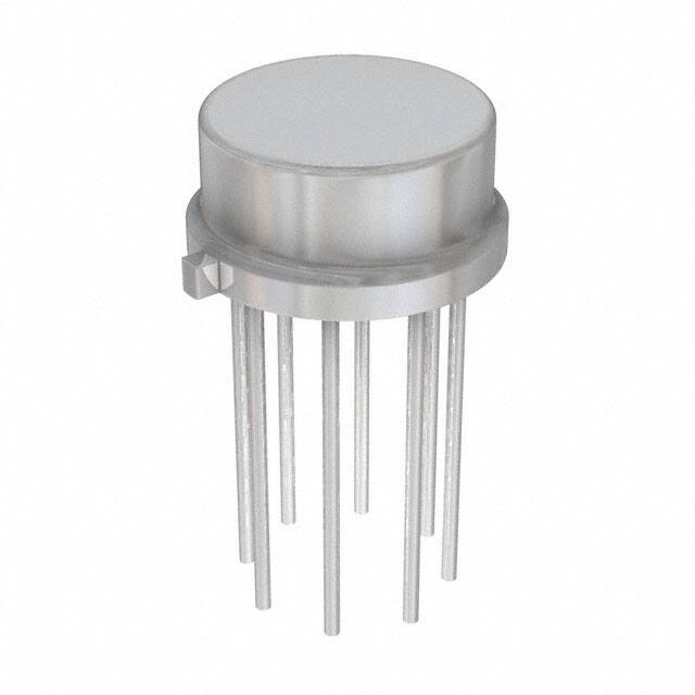
Device Information(1)
PART NUMBER
PACKAGE
BODY SIZE (NOM)
LF412ACN
PDIP
9.59 mm x 6.35 mm
LF412CN
PDIP
9.59 mm x 6.35 mm
LF412MH
TO
9.14 mm diameter
(1) For all available packages, see the orderable addendum at
the end of the datasheet.
Inverting Amplifier
1
An IMPORTANT NOTICE at the end of this data sheet addresses availability, warranty, changes, use in safety-critical applications,
intellectual property matters and other important disclaimers. PRODUCTION DATA.
�LF412-N
SNOSBH7F – APRIL 1999 – REVISED SEPTEMBER 2014
www.ti.com
Table of Contents
1
2
3
4
5
6
7
Features ..................................................................
Applications ...........................................................
Description .............................................................
Revision History.....................................................
Pin Configuration and Functions .........................
Specifications.........................................................
1
1
1
2
2
4
6.1
6.2
6.3
6.4
6.5
6.6
6.7
4
4
4
5
5
5
7
Absolute Maximum Ratings ......................................
Handling Ratings.......................................................
Recommended Operating Conditions.......................
Thermal Information ..................................................
DC Electrical Characteristics ...................................
AC Electrical Characteristics.....................................
Typical Characteristics ..............................................
Detailed Description ............................................ 12
7.1 Overview ................................................................. 12
7.2 Functional Block Diagram ....................................... 12
7.3 Feature Description................................................. 12
7.4 Device Functional Modes........................................ 13
8
Application and Implementation ........................ 14
8.1 Application Information............................................ 14
8.2 Typical Application ................................................. 14
9 Power Supply Recommendations...................... 16
10 Layout................................................................... 16
10.1 Layout Guidelines ................................................. 16
10.2 Layout Example .................................................... 16
11 Device and Documentation Support ................. 17
11.1 Trademarks ........................................................... 17
11.2 Electrostatic Discharge Caution ............................ 17
11.3 Glossary ................................................................ 17
12 Mechanical, Packaging, and Orderable
Information ........................................................... 17
4 Revision History
NOTE: Page numbers for previous revisions may differ from page numbers in the current version.
Changes from Revision E (March 2014) to Revision F
Page
•
Updated datasheet to new TI layout ...................................................................................................................................... 1
•
Deleted note. ......................................................................................................................................................................... 5
•
Deleted ΔVOS/ΔT Max specification for LF412A. ................................................................................................................... 5
•
Deleted ΔVOS/ΔT Max specification for LF412. ..................................................................................................................... 5
•
Added Application Note ........................................................................................................................................................ 14
Changes from Revision D (March 2013) to Revision E
•
Page
Changed layout of National Data Sheet to TI format ........................................................................................................... 14
5 Pin Configuration and Functions
TO Package
See Package Number NEV0008A
Top View
2
Submit Documentation Feedback
Copyright © 1999–2014, Texas Instruments Incorporated
Product Folder Links: LF412-N
�LF412-N
www.ti.com
SNOSBH7F – APRIL 1999 – REVISED SEPTEMBER 2014
PDIP/CDIP Package
See Package Number P0008E or NAB0008A
Top View
Pin Functions
PIN
NAME
NO.
I/O
DESCRIPTION
Output A
1
O
Amplifier A Output
Inverting
Input A
2
I
Amplifier A Inverting Input
Non-Inverting
Input A
3
I
Amplifier A Non-Inverting Input
V-
4
P
Negative Supply
Non-Inverting
Input B
5
I
Amplifier B Non-Inverting Input
Inverting
Input B
6
I
Amplifier B Inverting Input
Output B
7
O
Amplifier B Output
V+
8
P
Positive Supply
Submit Documentation Feedback
Copyright © 1999–2014, Texas Instruments Incorporated
Product Folder Links: LF412-N
3
�LF412-N
SNOSBH7F – APRIL 1999 – REVISED SEPTEMBER 2014
www.ti.com
6 Specifications
6.1 Absolute Maximum Ratings
over operating free-air temperature range (unless otherwise noted) (1) (2)
LF412A
LF412
UNIT
MIN
MAX
MIN
MAX
Supply Voltage
–22
22
–18
18
V
Differential Input Voltage
–38
38
–30
30
V
Input voltage Range (3)
Output Short Circuit Duration (4)
Power Dissipation (5)
See
Lead Temp. (Soldering, 10 sec.)
(5)
(6)
(7)
(6)
150
Operating Temp. Range
(2)
(3)
(4)
Continuous
PDIP Package
See
Tj max
(1)
Continuous
TO Package
(7)
670
mW
115
°C
See
260
(7)
260
°C
Stresses beyond those listed under Absolute Maximum Ratings may cause permanent damage to the device. These are stress ratings
only, which do not imply functional operation of the device at these or any other conditions beyond those indicated under Recommended
Operating Conditions. Exposure to absolute-maximum-rated conditions for extended periods may affect device reliability.
Refer to RETS412X for LF412MH and LF412MJ military specifications.
Unless otherwise specified the absolute maximum negative input voltage is equal to the negative power supply voltage.
Any of the amplifier outputs can be shorted to ground indefintely, however, more than one should not be simultaneously shorted as the
maximum junction temperature will be exceeded.
Max. Power Dissipation is defined by the package characteristics. Operating the part near the Max. Power Dissipation may cause the
part to operate outside guaranteed limits.
For operating at elevated temperature, these devices must be derated based on a thermal resistance of θjA.
These devices are available in both the commercial temperature range 0°C≤TA≤70°C and the military temperature range
−55°C≤TA≤125°C. The temperature range is designated by the position just before the package type in the device number. A “C”
indicates the commercial temperature range and an “M” indicates the military temperature range. The military temperature range is
available in TO package only. In all cases the maximum operating temperature is limited by internal junction temperature Tj max.
6.2 Handling Ratings
TO and PDIP Package
Tstg
Storage temperature range
V(ESD)
Electrostatic discharge
(1)
(2)
(3)
Human body model (HBM),
per ANSI/ESDA/JEDEC JS-001, all pins (1)
MIN
MAX
−65
150
-1700
1700 (2)
UNIT
°C
V
Charged device model (CDM),
per JEDEC specification JESD22-C101, all pins (3)
JEDEC document JEP155 states that 500-V HBM allows safe manufacturing with a standard ESD control process.
Human body model, 1.5 kΩ in series with 100 pF.
JEDEC document JEP157 states that 250-V CDM allows safe manufacturing with a standard ESD control process.
6.3 Recommended Operating Conditions
over operating free-air temperature range (unless otherwise noted)
MAX
UNIT
Supply Voltage LF412A
MIN
±20
V
Supply Voltage LF412
±15
V
4
Submit Documentation Feedback
NOM
Copyright © 1999–2014, Texas Instruments Incorporated
Product Folder Links: LF412-N
�LF412-N
www.ti.com
SNOSBH7F – APRIL 1999 – REVISED SEPTEMBER 2014
6.4 Thermal Information
THERMAL METRIC (1)
RθJA
Junction-to-ambient thermal resistance (Typical)
RθJC(top)
Junction-to-case (top) thermal resistance
RθJB
Junction-to-board thermal resistance
ψJT
Junction-to-top characterization parameter
ψJB
Junction-to-board characterization parameter
RθJC(bot)
Junction-to-case (bottom) thermal resistance
(1)
TO Package
PDIP Package
152
115
UNIT
°C/W
For more information about traditional and new thermal metrics, see the IC Package Thermal Metrics application report, SPRA953.
6.5 DC Electrical Characteristics
over operating free-air temperature range (unless otherwise noted)
PARAMETER
VOS
Input Offset Voltage
TEST CONDITIONS
LF412A (1)
MIN
RS=10 kΩ, TA=25°C
ΔVOS/Δ Average TC of Input
T
Offset Voltage
RS=10 kΩ
IOS
VS=±15V (1) (2)
TYP
MAX
0.5
1.0
25
Input Bias Current
RIN
Input Resistance
AVOL
Large Signal
Voltage Gain
VS=±15V (1) (2)
TYP
MAX
1.0
3.0
100
pA
2
2
nA
Tj=125°C
25
25
nA
50
25
mV
μV/°C
7
100
UNIT
Tj=70°C
Tj=25°C
IB
MIN
7
Tj=25°C
Input Offset Current
LF412 (1)
200
pA
Tj=70°C
200
4
50
4
nA
Tj=125°C
50
50
nA
1012
Tj=25°C
1012
Ω
RL=2k, TA=25°C, VS=±15V,
VO=±10V
50
200
25
200
Over Temperature
25
200
15
200
VS=±15V, RL=10k
±12
±13.5
±12
±13.5
V
±16
+19.5
±11
+14.5
V
−11.5
V
V/mV
VO
Output Voltage Swing
VCM
Input Common-Mode
Voltage Range
CMRR
Common-Mode
Rejection Ratio
RS≤10k
80
100
70
100
dB
PSRR
Supply Voltage
Rejection Ratio
See (3)
80
100
70
100
dB
IS
Supply Current
VO = 0V, RL = ∞
(1)
(2)
(3)
−16.5
3.6
5.6
3.6
6.5
mA
Unless otherwise specified, the specifications apply over the full temperature range and for VS=±20V for the LF412A and for VS=±15V
for the LF412. VOS, IB, and IOS are measured at VCM=0.
The input bias currents are junction leakage currents which approximately double for every 10°C increase in the junction temperature,
Tj. Due to limited production test time, the input bias currents measured are correlated to junction temperature. In normal operation the
junction temperature rises above the ambient temperature as a result of internal power dissipation, PD. Tj=TA+θjA PD where θjA is the
thermal resistance from junction to ambient. Use of a heat sink is recommended if input bias current is to be kept to a minimum.
Supply voltage rejection ratio is measured for both supply magnitudes increasing or decreasing simultaneously in accordance with
common practice. VS = ±6V to ±15V.
6.6 AC Electrical Characteristics
over operating free-air temperature range (unless otherwise noted)
PARAMETER
Amplifier to
Amplifier Coupling
(1)
TEST CONDITIONS
TA=25°C, f=1 Hz-20 kHz
(Input Referred)
LF412A (1)
MIN
TYP
−120
LF412 (1)
MAX
MIN
TYP
MAX
−120
UNIT
dB
Unless otherwise specified, the specifications apply over the full temperature range and for VS=±20V for the LF412A and for VS=±15V
for the LF412. VOS, IB, and IOS are measured at VCM=0.
Submit Documentation Feedback
Copyright © 1999–2014, Texas Instruments Incorporated
Product Folder Links: LF412-N
5
�LF412-N
SNOSBH7F – APRIL 1999 – REVISED SEPTEMBER 2014
www.ti.com
AC Electrical Characteristics (continued)
over operating free-air temperature range (unless otherwise noted)
PARAMETER
TEST CONDITIONS
LF412A (1)
MIN
TYP
LF412 (1)
MAX
MIN
TYP
MAX
UNIT
SR
Slew Rate
VS=±15V, TA=25°C
10
15
8
15
V/μs
GBW
Gain-Bandwidth Product
VS=±15V, TA=25°C
3
4
2.7
4
MHz
THD
Total Harmonic Dist
AV=+10, RL=10k,
VO=20 Vp-p,
BW=20 Hz-20 kHz
en
Equivalent Input
Noise Voltage
TA=25°C, RS=100Ω,
f=1 kHz
in
Equivalent Input
Noise Current
TA=25°C, f=1 kHz
6
≤0.02%
≤0.02%
25
25
nV /
√Hz
0.01
0.01
pA /
√Hz
Submit Documentation Feedback
Copyright © 1999–2014, Texas Instruments Incorporated
Product Folder Links: LF412-N
�LF412-N
www.ti.com
SNOSBH7F – APRIL 1999 – REVISED SEPTEMBER 2014
6.7 Typical Characteristics
Figure 2. Input Bias Current
Figure 1. Input Bias Current
Figure 3. Supply Current
Figure 4. Positive Common-Mode
Input Voltage Limit
Figure 5. Negative Common-Mode
Input Voltage Limit
Figure 6. Positive Current Limit
Submit Documentation Feedback
Copyright © 1999–2014, Texas Instruments Incorporated
Product Folder Links: LF412-N
7
�LF412-N
SNOSBH7F – APRIL 1999 – REVISED SEPTEMBER 2014
www.ti.com
Typical Characteristics (continued)
Figure 7. Negative Current Limit
Figure 8. Output Voltage Swing
Figure 10. Gain Bandwidth
Figure 9. Output Voltage Swing
Figure 11. Bode Plot
Figure 12. Slew Rate
8
Submit Documentation Feedback
Copyright © 1999–2014, Texas Instruments Incorporated
Product Folder Links: LF412-N
�LF412-N
www.ti.com
SNOSBH7F – APRIL 1999 – REVISED SEPTEMBER 2014
Typical Characteristics (continued)
Figure 13. Distortion vs
Frequency
Figure 14. Undistorted Output Voltage
Swing
Figure 15. Open Loop Frequency
Response
Figure 16. Common-Mode Rejection
Ratio
Figure 17. Power Supply Rejection
Ratio
Figure 18. Equivalent Input Noise
Voltage
Submit Documentation Feedback
Copyright © 1999–2014, Texas Instruments Incorporated
Product Folder Links: LF412-N
9
�LF412-N
SNOSBH7F – APRIL 1999 – REVISED SEPTEMBER 2014
www.ti.com
Typical Characteristics (continued)
10
Figure 19. Open Loop Voltage Gain
Figure 20. Output Impedance
Figure 21. Inverter Settling Time
Figure 22. Small Signal Inverting
(RL = 2 kΩ, CL = 10 pF)
Figure 23. Small Signal Non-Inverting
(RL = 2 kΩ, CL = 10 pF)
Figure 24. Large Signal Inverting
(RL = 2 kΩ, CL = 10 pF)
Submit Documentation Feedback
Copyright © 1999–2014, Texas Instruments Incorporated
Product Folder Links: LF412-N
�LF412-N
www.ti.com
SNOSBH7F – APRIL 1999 – REVISED SEPTEMBER 2014
Typical Characteristics (continued)
Figure 25. Large Signal Non-Inverting
(RL = 2 kΩ, CL = 10 pF)
Figure 26. Current Limit (RL=100Ω)
(CL = 10 pF)
Submit Documentation Feedback
Copyright © 1999–2014, Texas Instruments Incorporated
Product Folder Links: LF412-N
11
�LF412-N
SNOSBH7F – APRIL 1999 – REVISED SEPTEMBER 2014
www.ti.com
7 Detailed Description
7.1 Overview
The LF412 devices are low cost, high speed, JFET input operational amplifiers with very low input offset voltage
and input offset voltage drift. They require low supply current yet maintain a large gain bandwidth product and
fast slew rate. In addition, well matched high voltage JFET input devices provide very low input bias and offset
currents. The LF412-N dual is pin compatible with the LM1558, allowing designers to immediately upgrade the
overall performance of existing designs.
These amplifiers may be used in applications such as high speed integrators, fast D/A converters, sample and
hold circuits and many other circuits requiring low input offset voltage and drift, low input bias current, high input
impedance, high slew rate and wide bandwidth.
7.2 Functional Block Diagram
Figure 27. Each Amplifier
7.3 Feature Description
The amplifier's differential inputs consist of a non-inverting input (+IN) and an inverting input (-IN). The amplifier
amplifies only the difference in voltage between the two inputs, which is called the differential input voltage. The
output voltage of the op-amp VOUT is given by the equation VOUT = AOL(IN+ - IN-).
12
Submit Documentation Feedback
Copyright © 1999–2014, Texas Instruments Incorporated
Product Folder Links: LF412-N
�LF412-N
www.ti.com
SNOSBH7F – APRIL 1999 – REVISED SEPTEMBER 2014
7.4 Device Functional Modes
7.4.1 Input and Output Stage
Figure 28. 1/2 Dual LF412
Submit Documentation Feedback
Copyright © 1999–2014, Texas Instruments Incorporated
Product Folder Links: LF412-N
13
�LF412-N
SNOSBH7F – APRIL 1999 – REVISED SEPTEMBER 2014
www.ti.com
8 Application and Implementation
NOTE
Information in the following applications sections is not part of the TI component
specification, and TI does not warrant its accuracy or completeness. TI’s customers are
responsible for determining suitability of components for their purposes. Customers should
validate and test their design implementation to confirm system functionality.
8.1 Application Information
The LF412-N series of JFET input dual op amps are internally trimmed (BI-FET II™) providing very low input
offset voltages and input offset voltage drift. These JFETs have large reverse breakdown voltages from gate to
source and drain eliminating the need for clamps across the inputs. Therefore, large differential input voltages
can easily be accommodated without a large increase in input current. The maximum differential input voltage is
independent of the supply voltages. However, neither of the input voltages should be allowed to exceed the
negative supply as this will cause large currents to flow which can result in a destroyed unit.
8.2 Typical Application
Figure 29. Single Supply Sample and Hold
8.2.1 Design Requirements
Single supply.
8.2.2 Detailed Design Procedure
Exceeding the negative common-mode limit on either input will cause a reversal of the phase to the output and
force the amplifier output to the corresponding high or low state.
Exceeding the negative common-mode limit on both inputs will force the amplifier output to a high state. In
neither case does a latch occur since raising the input back within the common-mode range again puts the input
stage and thus the amplifier in a normal operating mode.
Exceeding the positive common-mode limit on a single input will not change the phase of the output, however, if
both inputs exceed the limit, the output of the amplifier may be forced to a high state.BI-FET II™
The amplifiers will operate with a common-mode input voltage equal to the positive supply; however, the gain
bandwidth and slew rate may be decreased in this condition. When the negative common-mode voltage swings
to within 3V of the negative supply, an increase in input offset voltage may occur.
Each amplifier is individually biased by a zener reference which allows normal circuit operation on ±6.0V power
supplies. Supply voltages less than these may result in lower gain bandwidth and slew rate.
The amplifiers will drive a 2 kΩ load resistance to ±10V over the full temperature range. If the amplifier is forced
to drive heavier load currents, however, an increase in input offset voltage may occur on the negative voltage
swing and finally reach an active current limit on both positive and negative swings.
14
Submit Documentation Feedback
Copyright © 1999–2014, Texas Instruments Incorporated
Product Folder Links: LF412-N
�LF412-N
www.ti.com
SNOSBH7F – APRIL 1999 – REVISED SEPTEMBER 2014
Typical Application (continued)
Precautions should be taken to ensure that the power supply for the integrated circuit never becomes reversed in
polarity or that the unit is not inadvertently installed backwards in a socket as an unlimited current surge through
the resulting forward diode within the IC could cause fusing of the internal conductors and result in a destroyed
unit.
As with most amplifiers, care should be taken with lead dress, component placement and supply decoupling in
order to ensure stability. For example, resistors from the output to an input should be placed with the body close
to the input to minimize “pick-up” and maximize the frequency of the feedback pole by minimizing the
capacitance from the input to ground.
A feedback pole is created when the feedback around any amplifier is resistive. The parallel resistance and
capacitance from the input of the device (usually the inverting input) to AC ground set the frequency of the pole.
In many instances the frequency of this pole is much greater than the expected 3 dB frequency of the closed
loop gain and consequently there is negligible effect on stability margin. However, if the feedback pole is less
than approximately 6 times the expected 3 dB frequency a lead capacitor should be placed from the output to the
input of the op amp. The value of the added capacitor should be such that the RC time constant of this capacitor
and the resistance it parallels is greater than or equal to the original feedback pole time constant.
8.2.3 Application Curves
10
8
(V)
6
4
2
Output
Input
Sample and Hold Signal
0
(2.5ms/DIV)
D001
Figure 30. Sample and Hold Waveforms
Submit Documentation Feedback
Copyright © 1999–2014, Texas Instruments Incorporated
Product Folder Links: LF412-N
15
�LF412-N
SNOSBH7F – APRIL 1999 – REVISED SEPTEMBER 2014
www.ti.com
9 Power Supply Recommendations
For proper operation, the power supplies must be properly decoupled. For decoupling the supply lines it is
suggested that 0.1µF capacitors be placed as close as possible to the op amp power supply pins. The minimum
power supply voltage is ±5V.
10 Layout
10.1 Layout Guidelines
As with most amplifiers, care should be taken with lead dress, component placement and supply decoupling in
order to ensure stability. For example, resistors from the output to an input should be placed with the body close
to the input to minimize “pick-up” and maximize the frequency of the feedback pole by minimizing the
capacitance from the input to ground.
10.2 Layout Example
Figure 31. LF412 Layout
16
Submit Documentation Feedback
Copyright © 1999–2014, Texas Instruments Incorporated
Product Folder Links: LF412-N
�LF412-N
www.ti.com
SNOSBH7F – APRIL 1999 – REVISED SEPTEMBER 2014
11 Device and Documentation Support
11.1 Trademarks
BI-FET II is a trademark of Texas Instruments.
All other trademarks are the property of their respective owners.
11.2 Electrostatic Discharge Caution
These devices have limited built-in ESD protection. The leads should be shorted together or the device placed in conductive foam
during storage or handling to prevent electrostatic damage to the MOS gates.
11.3 Glossary
SLYZ022 — TI Glossary.
This glossary lists and explains terms, acronyms, and definitions.
12 Mechanical, Packaging, and Orderable Information
The following pages include mechanical, packaging, and orderable information. This information is the most
current data available for the designated devices. This data is subject to change without notice and revision of
this document. For browser-based versions of this data sheet, refer to the left-hand navigation.
Submit Documentation Feedback
Copyright © 1999–2014, Texas Instruments Incorporated
Product Folder Links: LF412-N
17
�PACKAGE OPTION ADDENDUM
www.ti.com
25-Jun-2022
PACKAGING INFORMATION
Orderable Device
Status
(1)
Package Type Package Pins Package
Drawing
Qty
Eco Plan
(2)
Lead finish/
Ball material
MSL Peak Temp
Op Temp (°C)
Device Marking
(3)
Samples
(4/5)
(6)
LF412ACN/NOPB
ACTIVE
PDIP
P
8
40
RoHS & Green
NIPDAU
Level-1-NA-UNLIM
0 to 70
LF
412ACN
Samples
LF412CN/NOPB
ACTIVE
PDIP
P
8
40
RoHS & Green
NIPDAU
Level-1-NA-UNLIM
0 to 70
LF
412CN
Samples
(1)
The marketing status values are defined as follows:
ACTIVE: Product device recommended for new designs.
LIFEBUY: TI has announced that the device will be discontinued, and a lifetime-buy period is in effect.
NRND: Not recommended for new designs. Device is in production to support existing customers, but TI does not recommend using this part in a new design.
PREVIEW: Device has been announced but is not in production. Samples may or may not be available.
OBSOLETE: TI has discontinued the production of the device.
(2)
RoHS: TI defines "RoHS" to mean semiconductor products that are compliant with the current EU RoHS requirements for all 10 RoHS substances, including the requirement that RoHS substance
do not exceed 0.1% by weight in homogeneous materials. Where designed to be soldered at high temperatures, "RoHS" products are suitable for use in specified lead-free processes. TI may
reference these types of products as "Pb-Free".
RoHS Exempt: TI defines "RoHS Exempt" to mean products that contain lead but are compliant with EU RoHS pursuant to a specific EU RoHS exemption.
Green: TI defines "Green" to mean the content of Chlorine (Cl) and Bromine (Br) based flame retardants meet JS709B low halogen requirements of


 工商网监
湘ICP备2023018690号
工商网监
湘ICP备2023018690号
