LM101A-N, LM201A-N, LM301A-N
www.ti.com
SNOSBS0D – SEPTEMBER 1999 – REVISED MARCH 2013
LM101A/LM201A/LM301A Operational Amplifiers
Check for Samples: LM101A-N, LM201A-N, LM301A-N
FEATURES
DESCRIPTION
•
•
The LM101A series are general purpose operational
amplifiers which feature improved performance over
industry standards like the LM709. Advanced
processing techniques make possible an order of
magnitude reduction in input currents, and a redesign
of the biasing circuitry reduces the temperature drift
of input current.
1
•
•
•
•
•
Improved Specifications include:
Offset Voltage 3 mV Maximum Over
Temperature (LM101A/LM201A)
Input Current 100 nA Maximum Over
Temperature (LM101A/LM201A)
Offset Current 20 nA Maximum Over
Temperature (LM101A/LM201A)
Specified Drift Characteristics
Offsets Specified Over Entire Common Mode
and Supply Voltage Ranges
Slew Rate of 10V/μs as a Summing Amplifier
This amplifier offers many features which make its
application nearly foolproof: Overload protection on
the input and output, no latch-up when the common
mode range is exceeded, and freedom from
oscillations and compensation with a single 30 pF
Capacitor. It has advantages over internally
compensated amplifiers in that the frequency
compensation can be tailored to the particular
application. For example, in low frequency circuits it
can be overcompensated for increased stability
margin or the compensation can be optimized to give
more than a factor of ten improvement in high
frequency performance for most applications.
In Addition, the device provides better accuracy and
lower noise in high impedance circuitry. The low input
currents also make it particularly well suited for long
interval integrators or timers, sample and hold circuits
and low frequency waveform generators. Further,
replacing circuits where matched transistor pairs
buffer the inputs of conventional IC op amps, It can
give lower offset voltage and a drift at a lower cost.
The LM101A is ensured over a temperature range of
−55°C to +125°C, the LM201A from −25°C to +85°C,
and the LM301A from 0°C to +70°C.
Fast AC-DC Converter
1
Feedforward compensation can be used to make a fast full wave rectifier without a filter.
Please be aware that an important notice concerning availability, standard warranty, and use in critical applications of
Texas Instruments semiconductor products and disclaimers thereto appears at the end of this data sheet.
PRODUCTION DATA information is current as of publication date.
Products conform to specifications per the terms of the Texas
Instruments standard warranty. Production processing does not
necessarily include testing of all parameters.
Copyright © 1999–2013, Texas Instruments Incorporated
�LM101A-N, LM201A-N, LM301A-N
SNOSBS0D – SEPTEMBER 1999 – REVISED MARCH 2013
www.ti.com
These devices have limited built-in ESD protection. The leads should be shorted together or the device placed in conductive foam
during storage or handling to prevent electrostatic damage to the MOS gates.
Absolute Maximum Ratings (1) (2)
LM101A/LM201A
LM301A
Supply Voltage
±22V
±18V
Differential Input Voltage
±30V
±30V
Input Voltage
(3)
Output Short Circuit Duration (4)
Operating Ambient Temp. Range
±15V
±15V
Continuous
Continuous
−55°C to +125°C (LM101A)
0°C to +70°C
−25°C to +85°C (LM201A)
TJ Max
LMC0008C Package
150°C
100°C
P0008E Package
150°C
100°C
NAB0008A, J0014A Package
150°C
100°C
LMC0008C-Package (Still Air)
500 mW
300 mW
(400 LF/Min Air Flow)
1200 mW
700 mW
P0008E Package
900 mW
500 mW
NAB0008A, J0014A Package
1000 mW
650 mW
LMC0008C Package (Still Air)
165°C/W
165°C/W
(400 LF/Min Air Flow)
67°C/W
67°C/W
Power Dissipation at TA = 25°C
Thermal Resistance (Typical) θjA
P0008E Package
135°C/W
135°C/W
NAB0008A, J0014A Package
110°C/W
110°CmW
25°C/W
25°C/W
−65°C to +150°C
−65°C to +150°C
300°C
300°C
(Typical) θjC
LMC0008C Package
Storage Temperature Range
Lead Temperature (Soldering, 10 sec.)
LMC0008C or NAB0008A, J0014A, NAD0010A
P0008E
260°C
260°C
ESD Tolerance (5)
2000V
2000V
(1)
(2)
(3)
(4)
(5)
2
Absolute Maximum Ratings indicate limits beyond which damage to the device may occur. Operating ratings indicate for which the
device is functional, but do no ensure specific performance limits. Electrical Characteristics state DC and AC electrical specifications
under particular test conditions which ensure specific limits. This assumes that the device is within the Operating Ratings. Specifications
are not ensured for parameters where no limit is given, however, the typical value is a good indication of device performance.
If Military/Aerospace specified devices are required, please contact the Texas Instruments Sales Office/Distributors for availability and
specifications.
For supply voltages less than ±15V, the absolute maximum input voltage is equal to the supply voltage.
Continuous short circuit is allowed for case temperatures to 125°C and ambient temperatures to 75°C for LM101A/LM201A, and 70°C
and 55°C respectively for LM301A.
Human body model, 100 pF discharged through 1.5 kΩ.
Submit Documentation Feedback
Copyright © 1999–2013, Texas Instruments Incorporated
Product Folder Links: LM101A-N LM201A-N LM301A-N
�LM101A-N, LM201A-N, LM301A-N
www.ti.com
SNOSBS0D – SEPTEMBER 1999 – REVISED MARCH 2013
Electrical Characteristics (1)
TA= TJ
Parameter
Test Conditions
LM101A/LM201A
Min
LM301A
Typ
Max Min
Typ
Max
Units
Input Offset Voltage
TA = 25°C, RS ≤ 50 kΩ
0.7
2.0
2.0
7.5
mV
Input Offset Current
TA = 25°C
1.5
10
3.0
50
nA
Input Bias Current
TA = 25°C
30
75
70
250
nA
Input Resistance
TA = 25°C
Supply Current
TA = 25°C
1.5
VS = ±20V
4.0
1.8
0.5
TA = 25°C, VS = ±15V
1.8
50
MΩ
mA
VS = ±15V
Large Signal Voltage Gain
2.0
3.0
160
25
3.0
mA
160
V/mV
VOUT = ±10V, RL ≥ 2 kΩ
Input Offset Voltage
RS ≤ 50 kΩ
3.0
Average Temperature Coefficient of RS ≤ 50 kΩ
Input Offset Voltage
6.0
30
μV/°C
15
70
nA
0.01
0.1
0.01
0.3
nA/°C
0.02
0.2
0.02
0.6
nA/°C
20
Average Temperature Coefficient of 25°C ≤ TA ≤ TMAX
Input Offset Current
TMIN ≤ TA ≤ 25°C
Input Bias Current
0.1
Supply Current
TA = TMAX, VS = ±20V
Large Signal Voltage Gain
VS = ±15V, VOUT = ±10V
1.2
25
RL ≥ 2k
Input Voltage Range
mV
3.0
Input Offset Current
Output Voltage Swing
10
VS = ±15V
VS = ±20V
0.3
2.5
μA
mA
15
V/mV
RL = 10 kΩ
±12
±14
±12
±14
V
RL = 2 kΩ
±10
±13
±10
±13
V
±15
V
+15, −13
VS = ±15V
±12 +15, −13
V
Common-Mode Rejection Ratio
RS ≤ 50 kΩ
80
96
70
90
dB
Supply Voltage Rejection Ratio
RS ≤ 50 kΩ
80
96
70
96
dB
(1)
Unless otherwise specified, these specifications apply for C1 = 30 pF, ±5V ≤ VS ≤ ±20V and −55°C ≤ TA ≤ +125°C (LM101A), ±5V ≤ VS
≤ ±20V and −25°C ≤ TA ≤ +85°C (LM201A), ±5V ≤ VS ≤ ±15V and 0°C ≤ TA ≤ +70°C (LM301A).
Copyright © 1999–2013, Texas Instruments Incorporated
Product Folder Links: LM101A-N LM201A-N LM301A-N
Submit Documentation Feedback
3
�LM101A-N, LM201A-N, LM301A-N
SNOSBS0D – SEPTEMBER 1999 – REVISED MARCH 2013
www.ti.com
Typical Performance Characteristics
LM101A/LM201A
Input Voltage Range
Output Swing
Figure 1.
Figure 2.
Voltage Gain
Figure 3.
Performance Characteristics
LM301A
4
Input Voltage Range
Output Swing
Figure 4.
Figure 5.
Submit Documentation Feedback
Copyright © 1999–2013, Texas Instruments Incorporated
Product Folder Links: LM101A-N LM201A-N LM301A-N
�LM101A-N, LM201A-N, LM301A-N
www.ti.com
SNOSBS0D – SEPTEMBER 1999 – REVISED MARCH 2013
Performance Characteristics (continued)
LM301A
Voltage Gain
Figure 6.
Copyright © 1999–2013, Texas Instruments Incorporated
Product Folder Links: LM101A-N LM201A-N LM301A-N
Submit Documentation Feedback
5
�LM101A-N, LM201A-N, LM301A-N
SNOSBS0D – SEPTEMBER 1999 – REVISED MARCH 2013
www.ti.com
Typical Performance Characteristics
6
Supply Current
Voltage Gain
Figure 7.
Figure 8.
Maximum Power Dissipation
Input Current,
LM101A/LM201A/LM301A
Figure 9.
Figure 10.
Current Limiting
Input Noise Voltage
Figure 11.
Figure 12.
Submit Documentation Feedback
Copyright © 1999–2013, Texas Instruments Incorporated
Product Folder Links: LM101A-N LM201A-N LM301A-N
�LM101A-N, LM201A-N, LM301A-N
www.ti.com
SNOSBS0D – SEPTEMBER 1999 – REVISED MARCH 2013
Typical Performance Characteristics (continued)
Input Noise Current
Common Mode Rejection
Figure 13.
Figure 14.
Power Supply Rejection
Closed Loop Output
Impedance
Figure 15.
Figure 16.
Copyright © 1999–2013, Texas Instruments Incorporated
Product Folder Links: LM101A-N LM201A-N LM301A-N
Submit Documentation Feedback
7
�LM101A-N, LM201A-N, LM301A-N
SNOSBS0D – SEPTEMBER 1999 – REVISED MARCH 2013
www.ti.com
Typical Performance Characteristics for Various Compensation Circuits
Pin connections shown are for 8-pin packages.
CS= 30 pF
CS= 30 pF
C2 = 10 C1
Figure 17. Single Pole Compensation
Figure 18. Two Pole Compensation
Open Loop Frequency Response
fo= 3 MHz
8
Figure 19. Feedforward Compensation
Figure 20.
Open Loop Frequency Response
Open Loop Frequency Response
Figure 21.
Figure 22.
Submit Documentation Feedback
Copyright © 1999–2013, Texas Instruments Incorporated
Product Folder Links: LM101A-N LM201A-N LM301A-N
�LM101A-N, LM201A-N, LM301A-N
www.ti.com
SNOSBS0D – SEPTEMBER 1999 – REVISED MARCH 2013
Typical Performance Characteristics for Various Compensation Circuits (continued)
Large Signal Frequency Response
Large Signal Frequency Response
Figure 23.
Figure 24.
Large Signal Frequency Response
Voltage Follower Pulse Response
Figure 25.
Figure 26.
Voltage Follower Pulse Response
Inverter Pulse Response
Figure 27.
Figure 28.
Copyright © 1999–2013, Texas Instruments Incorporated
Product Folder Links: LM101A-N LM201A-N LM301A-N
Submit Documentation Feedback
9
�LM101A-N, LM201A-N, LM301A-N
SNOSBS0D – SEPTEMBER 1999 – REVISED MARCH 2013
www.ti.com
TYPICAL APPLICATIONS
Pin connections shown are for 8-pin packages
L ≃ R1 R2 C1
RS = R2
RP = R1
Figure 29. Variable Capacitance Multiplier
Figure 30. Simulated Inductor
Figure 31. Fast Inverting Amplifier with High
Input Impedance
fo = 10 kHz
Figure 33. Sine Wave Oscillator
†May be zero or equal to parallel
combination of R1 and R2 for minimum
offset.
Figure 32. Inverting Amplifier with Balancing
Circuit
*Adjust for zero integrator drift. Current drift
typically 0.1 nA/°C over −55°C to +125°C
temperature range.
Figure 34. Integrator with Bias Current
Compensation
10
Submit Documentation Feedback
Copyright © 1999–2013, Texas Instruments Incorporated
Product Folder Links: LM101A-N LM201A-N LM301A-N
�LM101A-N, LM201A-N, LM301A-N
www.ti.com
SNOSBS0D – SEPTEMBER 1999 – REVISED MARCH 2013
Application Hints
Pin connections shown are for 8-pin packages.
*Protects input
†Protects output
‡Protects output—not needed when R4 is used.
Figure 35. Protecting Against Gross Fault Conditions
Figure 36. Compensating for Stray Input Capacitances or Large Feedback Resistor
Figure 37. Isolating Large Capacitive Loads
Copyright © 1999–2013, Texas Instruments Incorporated
Product Folder Links: LM101A-N LM201A-N LM301A-N
Submit Documentation Feedback
11
�LM101A-N, LM201A-N, LM301A-N
SNOSBS0D – SEPTEMBER 1999 – REVISED MARCH 2013
www.ti.com
Although the LM101A is designed for trouble free operation, experience has indicated that it is wise to observe
certain precautions given below to protect the devices from abnormal operating conditions. It might be pointed
out that the advice given here is applicable to practically any IC op amp, although the exact reason why may
differ with different devices.
When driving either input from a low-impedance source, a limiting resistor should be placed in series with the
input lead to limit the peak instantaneous output current of the source to something less than 100 mA. This is
especially important when the inputs go outside a piece of equipment where they could accidentally be
connected to high voltage sources. Large capacitors on the input (greater than 0.1 μF) should be treated as a
low source impedance and isolated with a resistor. Low impedance sources do not cause a problem unless their
output voltage exceeds the supply voltage. However, the supplies go to zero when they are turned off, so the
isolation is usually needed.
The output circuitry is protected against damage from shorts to ground. However, when the amplifier output is
connected to a test point, it should be isolated by a limiting resistor, as test points frequently get shorted to bad
places. Further, when the amplifer drives a load external to the equipment, it is also advisable to use some sort
of limiting resistance to preclude mishaps.
Precautions should be taken to insure that the power supplies for the integrated circuit never become
reversed—even under transient conditions. With reverse voltages greater than 1V, the IC will conduct excessive
current, fusing internal aluminum interconnects. If there is a possibility of this happening, clamp diodes with a
high peak current rating should be installed on the supply lines. Reversal of the voltage between V+ and V− will
always cause a problem, although reversals with respect to ground may also give difficulties in many circuits.
The minimum values given for the frequency compensation capacitor are stable only for source resistances less
than 10 kΩ, stray capacitances on the summing junction less than 5 pF and capacitive loads smaller than 100
pF. If any of these conditions are not met, it becomes necessary to overcompensate the amplifier with a larger
compensation capacitor. Alternately, lead capacitors can be used in the feedback network to negate the effect of
stray capacitance and large feedback resistors or an RC network can be added to isolate capacitive loads.
Although the LM101A is relatively unaffected by supply bypassing, this cannot be ignored altogether. Generally it
is necessary to bypass the supplies to ground at least once on every circuit card, and more bypass points may
be required if more than five amplifiers are used. When feed-forward compensation is employed, however, it is
advisable to bypass the supply leads of each amplifier with low inductance capacitors because of the higher
frequencies involved.
12
Submit Documentation Feedback
Copyright © 1999–2013, Texas Instruments Incorporated
Product Folder Links: LM101A-N LM201A-N LM301A-N
�LM101A-N, LM201A-N, LM301A-N
www.ti.com
SNOSBS0D – SEPTEMBER 1999 – REVISED MARCH 2013
Typical Applications
Pin connections shown are for 8-pin packages.
Figure 38. Standard Compensation and Offset Balancing Circuit
Power Bandwidth: 15 kHz
Slew Rate: 1V/μs
Figure 39. Fast Voltage Follower
Power Bandwidth: 250 kHz
Small Signal Bandwiidth: 3.5 MHz
Slew Rate: 10V/μs
Figure 40. Fast Summing Amplifier
Copyright © 1999–2013, Texas Instruments Incorporated
Product Folder Links: LM101A-N LM201A-N LM301A-N
Submit Documentation Feedback
13
�LM101A-N, LM201A-N, LM301A-N
SNOSBS0D – SEPTEMBER 1999 – REVISED MARCH 2013
www.ti.com
R3 = R4 + R5
R1 = R2
Figure 41. Bilateral Current Source
Figure 42. Fast AC/DC Converter (1)
R1 = R4; R2 = R3
*,† Matching determines CMRR.
Figure 43. Instrumentation Amplifier
(1)
14
Feedforward compensation can be used to make a fast full wave rectifier without a filter
Submit Documentation Feedback
Copyright © 1999–2013, Texas Instruments Incorporated
Product Folder Links: LM101A-N LM201A-N LM301A-N
�LM101A-N, LM201A-N, LM301A-N
www.ti.com
SNOSBS0D – SEPTEMBER 1999 – REVISED MARCH 2013
*Adjust for zero integrator drift. Current drift typically 0.1 nA/°C over 0°C to +70°C temperature range.
Figure 44. Integrator with Bias Current Compensation
Figure 45. Voltage Comparator for Driving RTL Logic or High Current Driver
Figure 46. Low Frequency Square Wave Generator
*Polycarbonate-dielectric capacitor
Figure 47. Low Drift Sample and Hold
Copyright © 1999–2013, Texas Instruments Incorporated
Product Folder Links: LM101A-N LM201A-N LM301A-N
Submit Documentation Feedback
15
�LM101A-N, LM201A-N, LM301A-N
SNOSBS0D – SEPTEMBER 1999 – REVISED MARCH 2013
www.ti.com
Figure 48. Voltage Comparator for Driving DTL or TTL Integrated Circuits
Schematic
Pin connections shown are for 8-pin packages.
16
Submit Documentation Feedback
Copyright © 1999–2013, Texas Instruments Incorporated
Product Folder Links: LM101A-N LM201A-N LM301A-N
�LM101A-N, LM201A-N, LM301A-N
www.ti.com
SNOSBS0D – SEPTEMBER 1999 – REVISED MARCH 2013
Connection Diagrams
Top View
Top View
Figure 49. CDIP and PDIP Packages
Package Number NAB0008A or P0008E
Top View
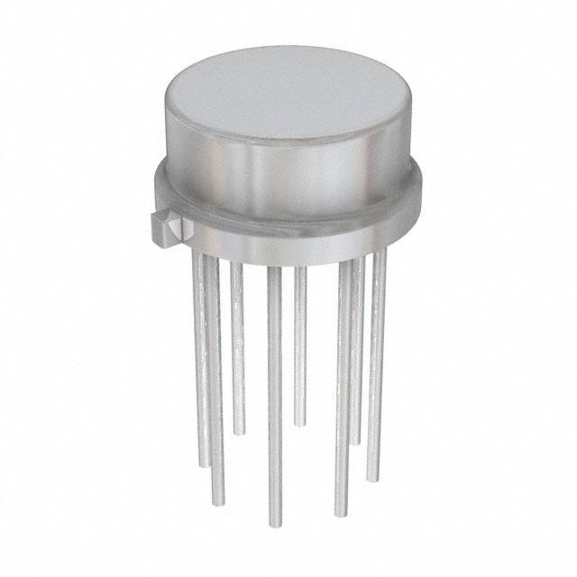
Figure 51. TO-99 Package
See Package Number LMC0008C
Top View
Figure 50. CLGA Package
Package Number NAD0010A
Figure 52. CDIP Package
See Package Number J0014A,
Copyright © 1999–2013, Texas Instruments Incorporated
Product Folder Links: LM101A-N LM201A-N LM301A-N
Submit Documentation Feedback
17
�LM101A-N, LM201A-N, LM301A-N
SNOSBS0D – SEPTEMBER 1999 – REVISED MARCH 2013
www.ti.com
REVISION HISTORY
Changes from Revision C (March 2013) to Revision D
•
18
Page
Changed layout of National Data Sheet to TI format .......................................................................................................... 17
Submit Documentation Feedback
Copyright © 1999–2013, Texas Instruments Incorporated
Product Folder Links: LM101A-N LM201A-N LM301A-N
�PACKAGE OPTION ADDENDUM
www.ti.com
30-Sep-2021
PACKAGING INFORMATION
Orderable Device
Status
(1)
Package Type Package Pins Package
Drawing
Qty
Eco Plan
(2)
Lead finish/
Ball material
MSL Peak Temp
Op Temp (°C)
Device Marking
(3)
(4/5)
(6)
LM101AH
ACTIVE
TO-99
LMC
8
500
Non-RoHS &
Non-Green
Call TI
Call TI
-55 to 125
( LM101AH, LM101AH
)
LM101AH/NOPB
ACTIVE
TO-99
LMC
8
500
RoHS & Green
Call TI
Level-1-NA-UNLIM
-55 to 125
( LM101AH, LM101AH
)
LM101AJ
ACTIVE
CDIP
NAB
8
40
Non-RoHS
& Green
Call TI
Level-1-NA-UNLIM
-55 to 125
LM101AJ
LM201AH
ACTIVE
TO-99
LMC
8
500
Non-RoHS &
Non-Green
Call TI
Call TI
-40 to 85
( LM201AH, LM201AH
)
LM201AH/NOPB
ACTIVE
TO-99
LMC
8
500
RoHS & Green
Call TI
Level-1-NA-UNLIM
-40 to 85
( LM201AH, LM201AH
)
LM301AH
ACTIVE
TO-99
LMC
8
500
Non-RoHS &
Non-Green
Call TI
Call TI
0 to 70
( LM301AH, LM301AH
)
LM301AH/NOPB
ACTIVE
TO-99
LMC
8
500
RoHS & Green
Call TI
Level-1-NA-UNLIM
0 to 70
( LM301AH, LM301AH
)
(1)
The marketing status values are defined as follows:
ACTIVE: Product device recommended for new designs.
LIFEBUY: TI has announced that the device will be discontinued, and a lifetime-buy period is in effect.
NRND: Not recommended for new designs. Device is in production to support existing customers, but TI does not recommend using this part in a new design.
PREVIEW: Device has been announced but is not in production. Samples may or may not be available.
OBSOLETE: TI has discontinued the production of the device.
(2)
RoHS: TI defines "RoHS" to mean semiconductor products that are compliant with the current EU RoHS requirements for all 10 RoHS substances, including the requirement that RoHS substance
do not exceed 0.1% by weight in homogeneous materials. Where designed to be soldered at high temperatures, "RoHS" products are suitable for use in specified lead-free processes. TI may
reference these types of products as "Pb-Free".
RoHS Exempt: TI defines "RoHS Exempt" to mean products that contain lead but are compliant with EU RoHS pursuant to a specific EU RoHS exemption.
Green: TI defines "Green" to mean the content of Chlorine (Cl) and Bromine (Br) based flame retardants meet JS709B low halogen requirements of


 工商网监
湘ICP备2023018690号
工商网监
湘ICP备2023018690号
