LM1577, LM2577
www.ti.com
SNOS658C – MAY 2004 – REVISED APRIL 2005
LM1577/LM2577 SIMPLE SWITCHER® Step-Up Voltage Regulator
Check for Samples: LM1577, LM2577
FEATURES
•
•
•
•
•
TYPICAL APPLICATIONS
1
23
•
•
Requires few external components
NPN output switches 3.0A, can stand off 65V
Wide input voltage range: 3.5V to 40V
Current-mode operation for improved transient
response, line regulation, and current limit
52 kHz internal oscillator
Soft-start function reduces in-rush current
during start-up
•
•
•
Output switch protected by current limit,
under-voltage lockout, and thermal shutdown
Simple boost regulator
Flyback and forward regulators
Multiple-output regulator
DESCRIPTION
The LM1577/LM2577 are monolithic integrated circuits that provide all of the power and control functions for
step-up (boost), flyback, and forward converter switching regulators. The device is available in three different
output voltage versions: 12V, 15V, and adjustable.
Requiring a minimum number of external components, these regulators are cost effective, and simple to use.
Listed in this data sheet are a family of standard inductors and flyback transformers designed to work with these
switching regulators.
Included on the chip is a 3.0A NPN switch and its associated protection circuitry, consisting of current and
thermal limiting, and undervoltage lockout. Other features include a 52 kHz fixed-frequency oscillator that
requires no external components, a soft start mode to reduce in-rush current during start-up, and current mode
control for improved rejection of input voltage and output load transients.
Connection Diagrams
Straight Leads
5-Lead TO-220 (T)
Figure 1. Top View
Order Number LM2577T-12, LM2577T-15,
or LM2577T-ADJ
See NS Package Number T05A
1
2
3
Please be aware that an important notice concerning availability, standard warranty, and use in critical applications of
Texas Instruments semiconductor products and disclaimers thereto appears at the end of this data sheet.
SIMPLE SWITCHER is a registered trademark of Texas Instruments.
All other trademarks are the property of their respective owners.
PRODUCTION DATA information is current as of publication date.
Products conform to specifications per the terms of the Texas
Instruments standard warranty. Production processing does not
necessarily include testing of all parameters.
Copyright © 2004–2005, Texas Instruments Incorporated
�LM1577, LM2577
SNOS658C – MAY 2004 – REVISED APRIL 2005
www.ti.com
Bent, Staggered Leads
5-Lead TO-220 (T)
Figure 2. Top View
Order Number LM2577T-12 Flow LB03, LM2577T-15
Flow LB03, or LM2577T-ADJ Flow LB03
See NS Package Number T05D
16-Lead DIP (N)
*No internal Connection
Figure 3. Top View
Order Number LM2577N-12, LM2577N-15,
or LM2577N-ADJ
See NS Package Number N16A
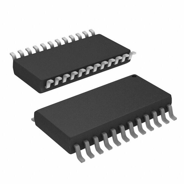
24-Lead Surface Mount (M)
*No internal Connection
Figure 4. Top View
Order Number LM2577M-12, LM2577M-15,
or LM2577M-ADJ
See NS Package Number M24B
2
Submit Documentation Feedback
Copyright © 2004–2005, Texas Instruments Incorporated
Product Folder Links: LM1577 LM2577
�LM1577, LM2577
www.ti.com
SNOS658C – MAY 2004 – REVISED APRIL 2005
TO-263 (S)
5-Lead Surface-Mount Package
Figure 5. Top View
Figure 6. Side View
Order Number LM2577S-12, LM2577S-15,
or LM2577S-ADJ
See NS Package Number TS5B
4-Lead TO-3 (K)
Figure 7. Bottom View
Order Number LM1577K-12/883, LM1577K-15/883,
or LM1577K-ADJ/883
See NS Package Number K04A
Typical Application
Note: Pin numbers shown are for TO-220 (T) package.
These devices have limited built-in ESD protection. The leads should be shorted together or the device placed in conductive foam
during storage or handling to prevent electrostatic damage to the MOS gates.
Submit Documentation Feedback
Copyright © 2004–2005, Texas Instruments Incorporated
Product Folder Links: LM1577 LM2577
3
�LM1577, LM2577
SNOS658C – MAY 2004 – REVISED APRIL 2005
Absolute Maximum Ratings
www.ti.com
(1)
Supply Voltage
45V
Output Switch Voltage
Output Switch Current
65V
(2)
6.0A
Power Dissipation
Internally Limited
Storage Temperature Range
−65°C to +150°C
Lead Temperature
(Soldering, 10 sec.)
260°C
Maximum Junction Temperature
150°C
Minimum ESD Rating
(C = 100 pF, R = 1.5 kΩ)
(1)
(2)
2 kV
Absolute Maximum Ratings indicate limits beyond which damage to the device may occur. Operating ratings indicate conditions the
device is intended to be functional, but device parameter specifications may not be guaranteed under these conditions. For guaranteed
specifications and test conditions, see the Electrical Characteristics.
Due to timing considerations of the LM1577/LM2577 current limit circuit, output current cannot be internally limited when the
LM1577/LM2577 is used as a step-up regulator. To prevent damage to the switch, its current must be externally limited to 6.0A.
However, output current is internally limited when the LM1577/LM2577 is used as a flyback or forward converter regulator in accordance
to the Application Hints.
Operating Ratings
3.5V ≤ VIN ≤ 40V
Supply Voltage
Output Switch Voltage
0V ≤ VSWITCH ≤ 60V
Output Switch Current
ISWITCH ≤ 3.0A
Junction Temperature Range
4
LM1577
−55°C ≤ TJ ≤ +150°C
LM2577
−40°C ≤ TJ ≤ +125°C
Submit Documentation Feedback
Copyright © 2004–2005, Texas Instruments Incorporated
Product Folder Links: LM1577 LM2577
�LM1577, LM2577
www.ti.com
SNOS658C – MAY 2004 – REVISED APRIL 2005
Electrical Characteristics—LM1577-12, LM2577-12
Specifications with standard type face are for TJ = 25°C, and those in bold type face apply over full Operating Temperature
Range. Unless otherwise specified, VIN = 5V, and ISWITCH = 0.
Symbol
Parameter
Conditions
Typical
LM1577-12
LM2577-12
Units
Limit
Limit
(Limits)
(1) (2) (3)
SYSTEM PARAMETERS Circuit of Figure 8
VOUT
Output Voltage
(4)
VIN = 5V to 10V
12.0
ILOAD = 100 mA to 800 mA
(1)
Line Regulation
VIN = 3.5V to 10V
V
11.60/11.40
11.60/11.40
V(min)
12.40/12.60
12.40/12.60
V(max)
50/100
50/100
mV(max)
20
ILOAD = 300 mA
mV
(1)
Load Regulation
VIN = 5V
20
ILOAD = 100 mA to 800 mA
mV
50/100
50/100
mV(max)
(2)
η
Efficiency
VIN = 5V, ILOAD = 800 mA
80
VFEEDBACK = 14V (Switch Off)
7.5
%
DEVICE PARAMETERS
IS
Input Supply Current
ISWITCH = 2.0A
Input Supply
ISWITCH = 100 mA
Oscillator Frequency
Measured at Switch Pin
Output Reference
Measured at Feedback Pin
Voltage
VIN = 3.5V to 40V
VIN = 3.5V to 40V
50/85
mA(max)
2.70/2.65
2.70/2.65
V(min)
3.10/3.15
3.10/3.15
V(max)
48/42
48/42
kHz(min)
56/62
56/62
kHz(max)
11.76/11.64
11.76/11.64
V(min)
12.24/12.36
12.24/12.36
V(max)
mA
V
kHz
V
12
VCOMP = 1.0V
Output Reference
50/85
52
ISWITCH = 100 mA
VREF
mA(max)
2.90
Undervoltage Lockout
fO
10.0/14.0
25
VCOMP = 2.0V (Max Duty Cycle)
VUV
mA
10.0/14.0
7
mV
9.7
kΩ
370
μmho
Voltage Line Regulator
(3)
RFB
Feedback Pin Input
Resistance
GM
(1)
(2)
(3)
(4)
Error Amp
ICOMP = −30 μA to +30 μA
Transconductance
VCOMP = 1.0V
225/145
225/145
μmho(min)
515/615
515/615
μmho(max)
All limits guaranteed at room temperature (standard type face) and at temperature extremes (boldface type). All limits are used to
calculate Outgoing Quality Level, and are 100% production tested.
A military RETS electrical test specification is available on request. At the time of printing, the LM1577K-12/883, LM1577K-15/883, and
LM1577K-ADJ/883 RETS specifications complied fully with the boldface limits in these columns. The LM1577K-12/883, LM1577K15/883, and LM1577K-ADJ/883 may also be procured to Standard Military Drawing specifications.
All limits guaranteed at room temperature (standard type face) and at temperature extremes (boldface type). All room temperature limits
are 100% production tested. All limits at temperature extremes are guaranteed via correlation using standard Statistical Quality Control
(SQC) methods.
External components such as the diode, inductor, input and output capacitors can affect switching regulator performance. When the
LM1577/LM2577 is used as shown in the Test Circuit, system performance will be as specified by the system parameters.
Submit Documentation Feedback
Copyright © 2004–2005, Texas Instruments Incorporated
Product Folder Links: LM1577 LM2577
5
�LM1577, LM2577
SNOS658C – MAY 2004 – REVISED APRIL 2005
www.ti.com
Electrical Characteristics—LM1577-12, LM2577-12 (continued)
Specifications with standard type face are for TJ = 25°C, and those in bold type face apply over full Operating Temperature
Range. Unless otherwise specified, VIN = 5V, and ISWITCH = 0.
Symbol
Parameter
Conditions
Typical
LM1577-12
LM2577-12
Units
Limit
Limit
(Limits)
(1) (2) (3)
AVOL
Error Amp
VCOMP = 1.1V to 1.9V
Voltage Gain
RCOMP = 1.0 MΩ
80
V/V
50/25
50/25
V/V(min)
2.2/2.0
2.2/2.0
V(min)
(5)
Error Amplifier
Upper Limit
Output Swing
VFEEDBACK = 10.0V
Lower Limit
2.4
0.3
VFEEDBACK = 15.0V
ISS
Error Amplifier
VFEEDBACK = 10.0V to 15.0V
Output Current
VCOMP = 1.0V
Soft Start Current
VFEEDBACK = 10.0V
Maximum Duty Cycle
VCOMP = 1.5V
0.40/0.55
0.40/0.55
V(max)
±130/±90
±130/±90
μA(min)
±300/±400
±300/±400
μA(max)
2.5/1.5
2.5/1.5
μA(min)
7.5/9.5
7.5/9.5
μA(max)
93/90
93/90
%(min)
μA
μA
5.0
95
ISWITCH = 100 mA
Switch
Transconductance
V
±200
VCOMP = 0V
D
V
%
12.5
A/V
(4)
IL
VSAT
Switch Leakage
VSWITCH = 65V
Current
VFEEDBACK = 15V (Switch Off)
Switch Saturation
ISWITCH = 2.0A
Voltage
VCOMP = 2.0V (Max Duty Cycle)
NPN Switch
6
300/600
300/600
μA(max)
0.7/0.9
0.7/0.9
V(max)
3.7/3.0
3.7/3.0
A(min)
5.3/6.0
5.3/6.0
A(max)
0.5
V
4.5
Current Limit
(5)
μA
10
A
A 1.0 MΩ resistor is connected to the compensation pin (which is the error amplifier's output) to ensure accuracy in measuring AVOL. In
actual applications, this pin's load resistance should be ≥10 MΩ, resulting in AVOL that is typically twice the guaranteed minimum limit.
Submit Documentation Feedback
Copyright © 2004–2005, Texas Instruments Incorporated
Product Folder Links: LM1577 LM2577
�LM1577, LM2577
www.ti.com
SNOS658C – MAY 2004 – REVISED APRIL 2005
Electrical Characteristics—LM1577-15, LM2577-15
Specifications with standard type face are for TJ = 25°C, and those in bold type face apply over full Operating Temperature
Range. Unless otherwise specified, VIN = 5V, and ISWITCH = 0.
Symbol
Parameter
Conditions
Typical
LM1577-15
LM2577-15
Units
Limit
Limit
(Limits)
(1) (2) (3)
SYSTEM PARAMETERS Circuit of Figure 9
VOUT
Output Voltage
(4)
VIN = 5V to 12V
15.0
ILOAD = 100 mA to 600 mA
(1)
Line Regulation
20
ILOAD = 300 mA
(5)
Load Regulation
VIN = 5V
20
ILOAD = 100 mA to 600 mA
(6)
η
VIN = 3.5V to 12V
Efficiency
VIN = 5V, ILOAD = 600 mA
80
VFEEDBACK = 18.0V
7.5
V
14.50/14.25
14.50/14.25
V(min)
15.50/15.75
15.50/15.75
V(max)
50/100
50/100
50/100
50/100
mV
mV(max)
mV
mV(max)
%
DEVICE PARAMETERS
IS
Input Supply Current
(Switch Off)
ISWITCH = 2.0A
mA
10.0/14.0
10.0/14.0
mA(max)
50/85
50/85
mA(max)
2.70/2.65
2.70/2.65
V(min)
3.10/3.15
3.10/3.15
V(max)
48/42
48/42
kHz(min)
56/62
56/62
kHz(max)
14.70/14.55
14.70/14.55
V(min)
15.30/15.45
15.30/15.45
V(max)
25
VCOMP = 2.0V
mA
(Max Duty Cycle)
VUV
Input Supply
ISWITCH = 100 mA
2.90
Undervoltage
Lockout
fO
Oscillator Frequency
Measured at Switch Pin
52
ISWITCH = 100 mA
VREF
Output Reference
Measured at Feedback Pin
Voltage
VIN = 3.5V to 40V
VIN = 3.5V to 40V
kHz
V
15
VCOMP = 1.0V
Output Reference
V
10
mV
12.2
kΩ
Voltage Line Regulation
RFB
Feedback Pin Input
Voltage Line Regulator
GM
AVOL
Error Amp
ICOMP = −30 μA to +30 μA
Transconductance
VCOMP = 1.0V
Error Amp
VCOMP = 1.1V to 1.9V
Voltage Gain
RCOMP = 1.0 MΩ
μmho
300
170/110
170/110
μmho(min)
420/500
420/500
μmho(max)
40/20
40/20
V/V(min)
65
V/V
(5)
(1)
(2)
(3)
(4)
(5)
All limits guaranteed at room temperature (standard type face) and at temperature extremes (boldface type). All limits are used to
calculate Outgoing Quality Level, and are 100% production tested.
A military RETS electrical test specification is available on request. At the time of printing, the LM1577K-12/883, LM1577K-15/883, and
LM1577K-ADJ/883 RETS specifications complied fully with the boldface limits in these columns. The LM1577K-12/883, LM1577K15/883, and LM1577K-ADJ/883 may also be procured to Standard Military Drawing specifications.
All limits guaranteed at room temperature (standard type face) and at temperature extremes (boldface type). All room temperature limits
are 100% production tested. All limits at temperature extremes are guaranteed via correlation using standard Statistical Quality Control
(SQC) methods.
External components such as the diode, inductor, input and output capacitors can affect switching regulator performance. When the
LM1577/LM2577 is used as shown in the Test Circuit, system performance will be as specified by the system parameters.
A 1.0 MΩ resistor is connected to the compensation pin (which is the error amplifier's output) to ensure accuracy in measuring AVOL. In
actual applications, this pin's load resistance should be ≥10 MΩ, resulting in AVOL that is typically twice the guaranteed minimum limit.
Submit Documentation Feedback
Copyright © 2004–2005, Texas Instruments Incorporated
Product Folder Links: LM1577 LM2577
7
�LM1577, LM2577
SNOS658C – MAY 2004 – REVISED APRIL 2005
www.ti.com
Electrical Characteristics—LM1577-15, LM2577-15 (continued)
Specifications with standard type face are for TJ = 25°C, and those in bold type face apply over full Operating Temperature
Range. Unless otherwise specified, VIN = 5V, and ISWITCH = 0.
Symbol
Parameter
Conditions
Typical
LM1577-15
LM2577-15
Units
Limit
Limit
(Limits)
(1) (2) (3)
Error Amplifier
Upper Limit
Output Swing
VFEEDBACK = 12.0V
Lower Limit
2.4
ISS
VFEEDBACK = 12.0V to 18.0V
Output Current
VCOMP = 1.0V
Soft Start Current
VFEEDBACK = 12.0V
Maximum Duty
VCOMP = 1.5V
Cycle
ISWITCH = 100 mA
Switch
Transconductance
V(min)
V
0.4/0.55
0.40/0.55
V(max)
±130/±90
±130/±90
μA(min)
±300/±400
±300/±400
μA(max)
2.5/1.5
2.5/1.5
μA(min)
7.5/9.5
7.5/9.5
μA(max)
93/90
93/90
%(min)
μA
±200
μA
5.0
VCOMP = 0V
D
2.2/2.0
0.3
VFEEDBACK = 18.0V
Error Amp
V
2.2/2.0
95
%
12.5
A/V
(7)
IL
Switch Leakage
VSWITCH = 65V
Current
VFEEDBACK = 18.0V
μA
10
300/600
300/600
μA(max)
0.7/0.9
0.7/0.9
V(max)
3.7/3.0
3.7/3.0
A(min)
5.3/6.0
5.3/6.0
A(max)
(Switch Off)
VSAT
Switch Saturation
ISWITCH = 2.0A
Voltage
VCOMP = 2.0V
0.5
V
(Max Duty Cycle)
NPN Switch
VCOMP = 2.0V
4.3
Current Limit
8
Submit Documentation Feedback
A
Copyright © 2004–2005, Texas Instruments Incorporated
Product Folder Links: LM1577 LM2577
�LM1577, LM2577
www.ti.com
SNOS658C – MAY 2004 – REVISED APRIL 2005
Electrical Characteristics—LM1577-ADJ, LM2577-ADJ
Specifications with standard type face are for TJ = 25°C, and those in bold type face apply over full Operating Temperature
Range. Unless otherwise specified, VIN = 5V, VFEEDBACK = VREF, and ISWITCH = 0.
Symbol
Parameter
Conditions
Typical
LM1577-ADJ
LM2577-ADJ
Units
Limit
Limit
(Limits)
(1) (2) (3)
SYSTEM PARAMETERS Circuit of Figure 10
VOUT
Output Voltage
(4)
VIN = 5V to 10V
12.0
ILOAD = 100 mA to 800 mA
(1)
ΔVOUT/
Line Regulation
ΔVIN
ΔVOUT/
Load Regulation
VIN = 5V
V(min)
12.40/12.60
12.40/12.60
V(max)
50/100
50/100
mV(max)
50/100
50/100
mV(max)
mV
20
ILOAD = 100 mA to 800 mA
Efficiency
11.60/11.40
20
ILOAD = 300 mA
ΔILOAD
η
VIN = 3.5V to 10V
V
11.60/11.40
VIN = 5V, ILOAD = 800 mA
80
VFEEDBACK = 1.5V (Switch Off)
7.5
mV
%
DEVICE PARAMETERS
IS
Input Supply Current
mA
10.0/14.0
ISWITCH = 2.0A
25
VCOMP = 2.0V (Max Duty Cycle)
VUV
Input Supply
ISWITCH = 100 mA
Oscillator Frequency
Measured at Switch Pin
VREF
Reference
Measured at Feedback Pin
Voltage
VIN = 3.5V to 40V
Reference Voltage
ΔVIN
Line Regulation
IB
Error Amp
AVOL
(1)
(2)
(3)
(4)
(5)
mA(max)
2.70/2.65
2.70/2.65
V(min)
3.10/3.15
3.10/3.15
V(max)
48/42
48/42
kHz(min)
56/62
56/62
kHz(max)
1.214/1.206
1.214/1.206
V(min)
1.246/1.254
1.246/1.254
V(max)
V
kHz
VIN = 3.5V to 40V
0.5
mV
VCOMP = 1.0V
100
nA
Error Amp
ICOMP = −30 μA to +30 μA
3700
Transconductance
VCOMP = 1.0V
Error Amp
VCOMP = 1.1V to 1.9V
Voltage Gain
RCOMP = 1.0 MΩ
Input Bias Current
GM
50/85
V
1.230
VCOMP = 1.0V
ΔVREF/
50/85
52
ISWITCH = 100 mA
mA(max)
mA
2.90
Undervoltage Lockout
fO
10.0/14.0
300/800
300/800
nA(max)
2400/1600
2400/1600
μmho(min)
4800/5800
4800/5800
μmho(max)
500/250
500/250
V/V(min)
μmho
800
(5)
V/V
All limits guaranteed at room temperature (standard type face) and at temperature extremes (boldface type). All limits are used to
calculate Outgoing Quality Level, and are 100% production tested.
A military RETS electrical test specification is available on request. At the time of printing, the LM1577K-12/883, LM1577K-15/883, and
LM1577K-ADJ/883 RETS specifications complied fully with the boldface limits in these columns. The LM1577K-12/883, LM1577K15/883, and LM1577K-ADJ/883 may also be procured to Standard Military Drawing specifications.
All limits guaranteed at room temperature (standard type face) and at temperature extremes (boldface type). All room temperature limits
are 100% production tested. All limits at temperature extremes are guaranteed via correlation using standard Statistical Quality Control
(SQC) methods.
External components such as the diode, inductor, input and output capacitors can affect switching regulator performance. When the
LM1577/LM2577 is used as shown in the Test Circuit, system performance will be as specified by the system parameters.
A 1.0 MΩ resistor is connected to the compensation pin (which is the error amplifier's output) to ensure accuracy in measuring AVOL. In
actual applications, this pin's load resistance should be ≥10 MΩ, resulting in AVOL that is typically twice the guaranteed minimum limit.
Submit Documentation Feedback
Copyright © 2004–2005, Texas Instruments Incorporated
Product Folder Links: LM1577 LM2577
9
�LM1577, LM2577
SNOS658C – MAY 2004 – REVISED APRIL 2005
www.ti.com
Electrical Characteristics—LM1577-ADJ, LM2577-ADJ (continued)
Specifications with standard type face are for TJ = 25°C, and those in bold type face apply over full Operating Temperature
Range. Unless otherwise specified, VIN = 5V, VFEEDBACK = VREF, and ISWITCH = 0.
Symbol
Parameter
Conditions
Typical
LM1577-ADJ
LM2577-ADJ
Units
Limit
Limit
(Limits)
(1) (2) (3)
Error Amplifier
Upper Limit
Output Swing
VFEEDBACK = 1.0V
2.4
Lower Limit
Error Amp
VFEEDBACK = 1.0V to 1.5V
Output Current
VCOMP = 1.0V
Soft Start Current
VFEEDBACK = 1.0V
Maximum Duty Cycle
VCOMP = 1.5V
ΔISWITCH/
Switch
ΔVCOMP
Transconductance
IL
Switch Leakage
VSWITCH = 65V
Current
VFEEDBACK = 1.5V (Switch Off)
Switch Saturation
ISWITCH = 2.0A
Voltage
VCOMP = 2.0V (Max Duty Cycle)
NPN Switch
VCOMP = 2.0V
VSAT
0.40/0.55
0.40/0.55
V(max)
±130/±90
±130/±90
μA(min)
±300/±400
±300/±400
μA(max)
2.5/1.5
2.5/1.5
μA(min)
7.5/9.5
7.5/9.5
μA(max)
93/90
93/90
%(min)
μA
μA
5.0
95
ISWITCH = 100 mA
%
12.5
A/V
μA
10
300/600
300/600
μA(max)
0.7/0.9
0.7/0.9
V(max)
0.5
V
4.3
Current Limit
V(min)
V
±200
VCOMP = 0V
D
2.2/2.0
0.3
VFEEDBACK = 1.5V
ISS
V
2.2/2.0
A
3.7/3.0
3.7/3.0
A(min)
5.3/6.0
5.3/6.0
A(max)
THERMAL PARAMETERS (All Versions)
θJA
Thermal Resistance
K Package, Junction to Ambient
35
θJC
K Package, Junction to Case
1.5
θJA
T Package, Junction to Ambient
65
θJC
T Package, Junction to Case
2
θJA
N Package, Junction to
85
Ambient
θJA
(6)
M Package, Junction
to Ambient
θJA
(6)
(7)
10
100
(6)
S Package, Junction to
Ambient
°C/W
37
(7)
Junction to ambient thermal resistance with approximately 1 square inch of pc board copper surrounding the leads. Additional copper
area will lower thermal resistance further. See thermal model in “Switchers Made Simple” software.
If the TO-263 package is used, the thermal resistance can be reduced by increasing the PC board copper area thermally connected to
the package. Using 0.5 square inches of copper area, θJA is 50°C/W; with 1 square inch of copper area, θJA is 37°C/W; and with 1.6 or
more square inches of copper area, θJA is 32°C/W.
Submit Documentation Feedback
Copyright © 2004–2005, Texas Instruments Incorporated
Product Folder Links: LM1577 LM2577
�LM1577, LM2577
www.ti.com
SNOS658C – MAY 2004 – REVISED APRIL 2005
Typical Performance Characteristics
Reference Voltage
vs Temperature
Reference Voltage
vs Temperature
Reference Voltage
vs Temperature
Δ Reference Voltage
vs Supply Voltage
Δ Reference Voltage
vs Supply Voltage
Δ Reference Voltage
vs Supply Voltage
Error Amp Transconductance
vs Temperature
Error Amp Transconductance
vs Temperature
Error Amp Transconductance
vs Temperature
Error Amp Voltage
Gain
vs
Temperature
Submit Documentation Feedback
Copyright © 2004–2005, Texas Instruments Incorporated
Product Folder Links: LM1577 LM2577
11
�LM1577, LM2577
SNOS658C – MAY 2004 – REVISED APRIL 2005
www.ti.com
Typical Performance Characteristics (continued)
12
Error Amp Voltage
Gain
vs
Temperature
Error Amp Voltage
Gain
vs
Temperature
Quiescent Current
vs Temperature
Quiescent Current
vs Switch Current
Current Limit
vs Temperature
Current Limit Response
Time
vs
Overdrive
Switch Saturation Voltage
vs Switch Current
Switch Transconductance
vs Temperature
Submit Documentation Feedback
Copyright © 2004–2005, Texas Instruments Incorporated
Product Folder Links: LM1577 LM2577
�LM1577, LM2577
www.ti.com
SNOS658C – MAY 2004 – REVISED APRIL 2005
Typical Performance Characteristics (continued)
Feedback Pin Bias
Current
vs
Temperature
Oscillator Frequency
vs Temperature
Maximum Power Dissipation
(TO-263) (1)
LM1577-12, LM2577-12 Test Circuit
L = 415-0930 (AIE)
D = any manufacturer
COUT = Sprague Type 673D
Electrolytic 680 μF, 20V
Note: Pin numbers shown are for TO-220 (T) package
Figure 8. Circuit Used to Specify System Parameters for 12V Versions
(1)
If the TO-263 package is used, the thermal resistance can be reduced by increasing the PC board copper area thermally connected to
the package. Using 0.5 square inches of copper area, θJA is 50°C/W; with 1 square inch of copper area, θJA is 37°C/W; and with 1.6 or
more square inches of copper area, θJA is 32°C/W.
Submit Documentation Feedback
Copyright © 2004–2005, Texas Instruments Incorporated
Product Folder Links: LM1577 LM2577
13
�LM1577, LM2577
SNOS658C – MAY 2004 – REVISED APRIL 2005
www.ti.com
LM1577-15, LM2577-15 Test Circuit
L = 415-0930 (AIE)
D = any manufacturer
COUT = Sprague Type 673D
Electrolytic 680 μF, 20V
Note: Pin numbers shown are for TO-220 (T) package
Figure 9. Circuit Used to Specify System Parameters for 15V Versions
LM1577-ADJ, LM2577-ADJ Test Circuit
L = 415-0930 (AIE)
D = any manufacturer
COUT = Sprague Type 673D
Electrolytic 680 μF, 20V
R1 = 48.7k in series with 511Ω (1%)
R2 = 5.62k (1%)
Note: Pin numbers shown are for TO-220 (T) package
Figure 10. Circuit Used to Specify System Parameters for ADJ Versions
14
Submit Documentation Feedback
Copyright © 2004–2005, Texas Instruments Incorporated
Product Folder Links: LM1577 LM2577
�LM1577, LM2577
www.ti.com
SNOS658C – MAY 2004 – REVISED APRIL 2005
Application Hints
Note: Pin numbers shown are for TO-220 (T) package
*Resistors are internal to LM1577/LM2577 for 12V and 15V versions.
Figure 11. LM1577/LM2577 Block Diagram and Boost Regulator Application
STEP-UP (BOOST) REGULATOR
Figure 11 shows the LM1577-ADJ/LM2577-ADJ used as a Step-Up Regulator. This is a switching regulator used
for producing an output voltage greater than the input supply voltage. The LM1577-12/LM2577-12 and LM157715/LM2577-15 can also be used for step-up regulators with 12V or 15V outputs (respectively), by tying the
feedback pin directly to the regulator output.
A basic explanation of how it works is as follows. The LM1577/LM2577 turns its output switch on and off at a
frequency of 52 kHz, and this creates energy in the inductor (L). When the NPN switch turns on, the inductor
current charges up at a rate of VIN/L, storing current in the inductor. When the switch turns off, the lower end of
the inductor flies above VIN, discharging its current through diode (D) into the output capacitor (COUT) at a rate of
(VOUT − VIN)/L. Thus, energy stored in the inductor during the switch on time is transferred to the output during
the switch off time. The output voltage is controlled by the amount of energy transferred which, in turn, is
controlled by modulating the peak inductor current. This is done by feeding back a portion of the output voltage
to the error amp, which amplifies the difference between the feedback voltage and a 1.230V reference. The error
amp output voltage is compared to a voltage proportional to the switch current (i.e., inductor current during the
switch on time).
The comparator terminates the switch on time when the two voltages are equal, thereby controlling the peak
switch current to maintain a constant output voltage.
Voltage and current waveforms for this circuit are shown in Figure 12, and formulas for calculating them are
given in Table 1.
Submit Documentation Feedback
Copyright © 2004–2005, Texas Instruments Incorporated
Product Folder Links: LM1577 LM2577
15
�LM1577, LM2577
SNOS658C – MAY 2004 – REVISED APRIL 2005
www.ti.com
Figure 12. Step-Up Regulator Waveforms
Table 1. Step-Up Regulator Formulas
Duty Cycle
D
Average Inductor Current
Inductor Current Ripple
Peak Inductor Current
Peak Switch Current
Switch Voltage When Off
IIND(AVE)
ΔIIND
IIND(PK)
ISW(PK)
VSW(OFF)
VOUT + VF
Diode Reverse Voltage
VR
VOUT − VSAT
Average Diode Current
ID(AVE)
ILOAD
Peak Diode Current
Power Dissipation of LM1577/2577
ID(PK)
PD
STEP-UP REGULATOR DESIGN PROCEDURE
The following design procedure can be used to select the appropriate external components for the circuit in
Figure 11, based on these system requirements.
Given:
VIN
(min)
= Minimum input supply voltage
VOUT = Regulated output voltage
ILOAD(max) = Maximum output load current
Before proceeding any further, determine if the LM1577/LM2577 can provide these values of VOUT and ILOAD(max)
when operating with the minimum value of VIN. The upper limits for VOUT and ILOAD(max) are given by the following
equations.
VOUT ≤ 60V
and
VOUT ≤ 10 × VIN(min)
(8)
These limits must be greater than or equal to the values specified in this application.
1.
Inductor Selection (L)
A. Voltage Options:
1. For 12V or 15V output
16
Submit Documentation Feedback
Copyright © 2004–2005, Texas Instruments Incorporated
Product Folder Links: LM1577 LM2577
�LM1577, LM2577
www.ti.com
SNOS658C – MAY 2004 – REVISED APRIL 2005
From Figure 13 (for 12V output) or Figure 14 (for 15V output), identify inductor code for region
indicated by VIN (min) and ILOAD (max). The shaded region indicates conditions for which the LM1577/LM2577
output switch would be operating beyond its switch current rating. The minimum operating voltage for the
LM1577/LM2577 is 3.5V.
From here, proceed to step C.
2. For Adjustable version
Preliminary calculations:
The inductor selection is based on the calculation of the following three parameters:
D(max), the maximum switch duty cycle (0 ≤ D ≤ 0.9):
(9)
where VF = 0.5V for Schottky diodes and 0.8V for fast recovery diodes (typically);
E •T, the product of volts × time that charges the inductor:
(10)
IIND,DC, the average inductor current under full load;
(11)
B.
Identify Inductor Value:
1. From Figure 15, identify the inductor code for the region indicated by the intersection of E•T and IIND,DC.
This code gives the inductor value in microhenries. The L or H prefix signifies whether the inductor is rated
for a maximum E•T of 90 V•μs (L) or 250 V•μs (H).
2. If D < 0.85, go on to step C. If D ≥ 0.85, then calculate the minimum inductance needed to ensure the
switching regulator's stability:
(12)
If LMIN is smaller than the inductor value found in step B1, go on to step C. Otherwise, the inductor value found in
step B1 is too low; an appropriate inductor code should be obtained from the graph as follows:
1. Find the lowest value inductor that is greater than LMIN.
2. Find where E•T intersects this inductor value to determine if it has an L or H prefix. If E•T intersects both the L
and H regions, select the inductor with an H prefix.
Figure 13. LM2577-12 Inductor Selection Guide
Submit Documentation Feedback
Copyright © 2004–2005, Texas Instruments Incorporated
Product Folder Links: LM1577 LM2577
17
�LM1577, LM2577
SNOS658C – MAY 2004 – REVISED APRIL 2005
www.ti.com
Figure 14. LM2577-15 Inductor Selection Guide
Note: These charts assume that the inductor ripple current inductor is approximately 20% to 30% of the average
inductor current (when the regulator is under full load). Greater ripple current causes higher peak switch currents and
greater output ripple voltage; lower ripple current is achieved with larger-value inductors. The factor of 20 to 30% is
chosen as a convenient balance between the two extremes.
Figure 15. LM1577-ADJ/LM2577-ADJ Inductor Selection Graph
C.
Select an inductor from the table of Table 2 which cross-references the inductor codes to the part
numbers of three different manufacturers. Complete specifications for these inductors are available from
the respective manufacturers. The inductors listed in this table have the following characteristics:
AIE: ferrite, pot-core inductors; Benefits of this type are low electro-magnetic interference (EMI), small
physical size, and very low power dissipation (core loss). Be careful not to operate these inductors too far
beyond their maximum ratings for E•T and peak current, as this will saturate the core.
Pulse: powdered iron, toroid core inductors; Benefits are low EMI and ability to withstand E•T and peak
current above rated value better than ferrite cores.
Renco: ferrite, bobbin-core inductors; Benefits are low cost and best ability to withstand E•T and peak
current above rated value. Be aware that these inductors generate more EMI than the other types, and
this may interfere with signals sensitive to noise.
18
Submit Documentation Feedback
Copyright © 2004–2005, Texas Instruments Incorporated
Product Folder Links: LM1577 LM2577
�LM1577, LM2577
www.ti.com
SNOS658C – MAY 2004 – REVISED APRIL 2005
Table 2. Table of Standardized Inductors and
Manufacturer's Part Numbers
Inductor
Manufacturer's Part Number
Code
Schott
Pulse
Renco
L47
67126980
PE - 53112
RL2442
L68
67126990
PE - 92114
RL2443
L100
67127000
PE - 92108
RL2444
L150
67127010
PE - 53113
RL1954
L220
67127020
PE - 52626
RL1953
L330
67127030
PE - 52627
RL1952
L470
67127040
PE - 53114
RL1951
L680
67127050
PE - 52629
RL1950
H150
67127060
PE - 53115
RL2445
H220
67127070
PE - 53116
RL2446
H330
67127080
PE - 53117
RL2447
H470
67127090
PE - 53118
RL1961
H680
67127100
PE - 53119
RL1960
H1000
67127110
PE - 53120
RL1959
H1500
67127120
PE - 53121
RL1958
H2200
67127130
PE - 53122
RL2448
2. Compensation Network (RC, CC) and Output Capacitor (COUT) Selection
RC and CC form a pole-zero compensation network that stabilizes the regulator. The values of RC and CC are
mainly dependant on the regulator voltage gain, ILOAD(max), L and COUT. The following procedure calculates values
for RC, CC, and COUT that ensure regulator stability. Be aware that this procedure doesn't necessarily result in RC
and CC that provide optimum compensation. In order to guarantee optimum compensation, one of the standard
procedures for testing loop stability must be used, such as measuring VOUT transient response when pulsing
ILOAD (see Figure 18).
A. First, calculate the maximum value for RC.
(13)
Select a resistor less than or equal to this value, and it should also be no greater than 3 kΩ.
B. Calculate the minimum value for COUT using the following two equations.
(14)
The larger of these two values is the minimum value that ensures stability.
C. Calculate the minimum value of CC .
(15)
The compensation capacitor is also part of the soft start circuitry. When power to the regulator is turned on, the
switch duty cycle is allowed to rise at a rate controlled by this capacitor (with no control on the duty cycle, it
would immediately rise to 90%, drawing huge currents from the input power supply). In order to operate properly,
the soft start circuit requires CC ≥ 0.22 μF.
The value of the output filter capacitor is normally large enough to require the use of aluminum electrolytic
capacitors. Table 3 lists several different types that are recommended for switching regulators, and the following
parameters are used to select the proper capacitor.
Submit Documentation Feedback
Copyright © 2004–2005, Texas Instruments Incorporated
Product Folder Links: LM1577 LM2577
19
�LM1577, LM2577
SNOS658C – MAY 2004 – REVISED APRIL 2005
www.ti.com
Working Voltage (WVDC): Choose a capacitor with a working voltage at least 20% higher than the regulator
output voltage.
Ripple Current: This is the maximum RMS value of current that charges the capacitor during each switching
cycle. For step-up and flyback regulators, the formula for ripple current is
(16)
Choose a capacitor that is rated at least 50% higher than this value at 52 kHz.
Equivalent Series Resistance (ESR) : This is the primary cause of output ripple voltage, and it also affects the
values of RC and CC needed to stabilize the regulator. As a result, the preceding calculations for CC and RC are
only valid if ESR doesn't exceed the maximum value specified by the following equations.
(17)
Select a capacitor with ESR, at 52 kHz, that is less than or equal to the lower value calculated. Most electrolytic
capacitors specify ESR at 120 Hz which is 15% to 30% higher than at 52 kHz. Also, be aware that ESR
increases by a factor of 2 when operating at −20°C.
In general, low values of ESR are achieved by using large value capacitors (C ≥ 470 μF), and capacitors with
high WVDC, or by paralleling smaller-value capacitors.
3. Output Voltage Selection (R1 and R2)
This section is for applications using the LM1577-ADJ/LM2577-ADJ. Skip this section if the LM1577-12/LM257712 or LM1577-15/LM2577-15 is being used.
With the LM1577-ADJ/LM2577-ADJ, the output voltage is given by
VOUT = 1.23V (1 + R1/R2)
(18)
Resistors R1 and R2 divide the output down so it can be compared with the LM1577-ADJ/LM2577-ADJ internal
1.23V reference. For a given desired output voltage VOUT, select R1 and R2 so that
(19)
4. Input Capacitor Selection (CIN)
The switching action in the step-up regulator causes a triangular ripple current to be drawn from the supply
source. This in turn causes noise to appear on the supply voltage. For proper operation of the LM1577, the input
voltage should be decoupled. Bypassing the Input Voltage pin directly to ground with a good quality, low ESR,
0.1 μF capacitor (leads as short as possible) is normally sufficient.
20
Submit Documentation Feedback
Copyright © 2004–2005, Texas Instruments Incorporated
Product Folder Links: LM1577 LM2577
�LM1577, LM2577
www.ti.com
SNOS658C – MAY 2004 – REVISED APRIL 2005
Table 3. Aluminum Electrolytic Capacitors
Recommended for Switching Regulators
Cornell Dublier —Types 239, 250, 251, UFT, 300, or 350
P.O. Box 128, Pickens, SC 29671
(803) 878-6311
Nichicon —Types PF, PX, or PZ
927 East Parkway,
Schaumburg, IL 60173
(708) 843-7500
Sprague —Types 672D, 673D, or 674D
Box 1, Sprague Road,
Lansing, NC 28643
(919) 384-2551
United Chemi-Con —Types LX, SXF, or SXJ
9801 West Higgins Road,
Rosemont, IL 60018
(708) 696-2000
If the LM1577 is located far from the supply source filter capacitors, an additional large electrolytic capacitor (e.g.
47 μF) is often required.
5. Diode Selection (D)
The switching diode used in the boost regulator must withstand a reverse voltage equal to the circuit output
voltage, and must conduct the peak output current of the LM2577. A suitable diode must have a minimum
reverse breakdown voltage greater than the circuit output voltage, and should be rated for average and peak
current greater than ILOAD(max) and ID(PK). Schottky barrier diodes are often favored for use in switching regulators.
Their low forward voltage drop allows higher regulator efficiency than if a (less expensive) fast recovery diode
was used. See Table 4 for recommended part numbers and voltage ratings of 1A and 3A diodes.
Table 4. Diode Selection Chart
VOUT
Schottky
Fast Recovery
(max)
1A
3A
20V
1N5817
1N5820
MBR120P
MBR320P
30V
40V
50V
1N5818
1N5821
MBR130P
MBR330P
11DQ03
31DQ03
1N5819
1N5822
MBR140P
MBR340P
1A
11DQ04
31DQ04
MBR150
MBR350
1N4933
11DQ05
31DQ05
MUR105
1N4934
100V
3A
MR851
HER102
30DL1
MUR110
MR831
10DL1
HER302
BOOST REGULATOR CIRCUIT EXAMPLE
By adding a few external components (as shown in Figure 16), the LM2577 can be used to produce a regulated
output voltage that is greater than the applied input voltage. Typical performance of this regulator is shown in
Figure 17 and Figure 18. The switching waveforms observed during the operation of this circuit are shown in
Figure 19.
Submit Documentation Feedback
Copyright © 2004–2005, Texas Instruments Incorporated
Product Folder Links: LM1577 LM2577
21
�LM1577, LM2577
SNOS658C – MAY 2004 – REVISED APRIL 2005
www.ti.com
Note: Pin numbers shown are for TO-220 (T) package.
Figure 16. Step-up Regulator Delivers 12V from a 5V Input
Figure 17. Line Regulation (Typical) of Step-Up Regulator of Figure 16
A: Output Voltage Change, 100 mV/div. (AC-coupled)
B: Load current, 0.2 A/div
Horizontal: 5 ms/div
Figure 18. Load Transient Response of Step-Up
Regulator of Figure 16
22
Submit Documentation Feedback
Copyright © 2004–2005, Texas Instruments Incorporated
Product Folder Links: LM1577 LM2577
�LM1577, LM2577
www.ti.com
SNOS658C – MAY 2004 – REVISED APRIL 2005
A: Switch pin voltage, 10 V/div
B: Switch pin current, 2 A/div
C: Inductor current, 2 A/div
D: Output ripple voltage, 100 mV/div (AC-coupled)
Horizontal: 5 μs/div
Figure 19. Switching Waveforms of Step-Up
Regulator of Figure 16
FLYBACK REGULATOR
A Flyback regulator can produce single or multiple output voltages that are lower or greater than the input supply
voltage. Figure 21 shows the LM1577/LM2577 used as a flyback regulator with positive and negative regulated
outputs. Its operation is similar to a step-up regulator, except the output switch contols the primary current of a
flyback transformer. Note that the primary and secondary windings are out of phase, so no current flows through
secondary when current flows through the primary. This allows the primary to charge up the transformer core
when the switch is on. When the switch turns off, the core discharges by sending current through the secondary,
and this produces voltage at the outputs. The output voltages are controlled by adjusting the peak primary
current, as described in the step-up regulator section.
Voltage and current waveforms for this circuit are shown in Figure 20, and formulas for calculating them are
given in Figure 22.
FLYBACK REGULATOR DESIGN PROCEDURE
1. Transformer Selection
A family of standardized flyback transformers is available for creating flyback regulators that produce dual output
voltages, from ±10V to ±15V, as shown in Figure 21. Table 5lists these transformers with the input voltage,
output voltages and maximum load current they are designed for.
2. Compensation Network (CC, RC) and
Output Capacitor (COUT) Selection
As explained in the Step-Up Regulator Design Procedure, CC, RC and COUT must be selected as a group. The
following procedure is for a dual output flyback regulator with equal turns ratios for each secondary (i.e., both
output voltages have the same magnitude). The equations can be used for a single output regulator by changing
∑ILOAD(max) to ILOAD(max) in the following equations.
A. First, calculate the maximum value for RC.
Submit Documentation Feedback
Copyright © 2004–2005, Texas Instruments Incorporated
Product Folder Links: LM1577 LM2577
23
�LM1577, LM2577
SNOS658C – MAY 2004 – REVISED APRIL 2005
www.ti.com
(20)
Where ∑ILOAD(max) is the sum of the load current (magnitude) required from both outputs. Select a resistor less
than or equal to this value, and no greater than 3 kΩ.
B. Calculate the minimum value for ∑COUT (sum of COUT at both outputs) using the following two equations.
(21)
The larger of these two values must be used to ensure regulator stability.
Figure 20. Flyback Regulator Waveforms
T1 = Pulse Engineering, PE-65300
D1, D2 = 1N5821
Figure 21. LM1577-ADJ/LM2577-ADJ Flyback Regulator with ± Outputs
Duty Cycle
D
(22)
Primary Current Variation
ΔIP
(23)
Peak Primary Current
IP(PK)
24
Submit Documentation Feedback
(24)
Copyright © 2004–2005, Texas Instruments Incorporated
Product Folder Links: LM1577 LM2577
�LM1577, LM2577
www.ti.com
SNOS658C – MAY 2004 – REVISED APRIL 2005
Switch Voltage when Off
VSW(OFF)
(25)
−
+
Diode Reverse Voltage
VR
VOUT N (VIN VSAT)
Average Diode Current
ID(AVE)
ILOAD
Peak Diode Current
ID(PK)
(26)
Short Circuit Diode Current
(27)
Power Dissipation of LM1577/LM2577
PD
(28)
Figure 22. Flyback Regulator Formulas
C. Calculate the minimum value of CC
(29)
D. Calculate the maximum ESR of the +VOUT and −VOUT output capacitors in parallel.
(30)
This formula can also be used to calculate the maximum ESR of a single output regulator.
At this point, refer to this same section in the Step-Up Regulator Design Procedurefor more information
regarding the selection of COUT.
3. Output Voltage Selection
This section is for applications using the LM1577-ADJ/LM2577-ADJ. Skip this section if the LM1577-12/LM257712 or LM1577-15/LM2577-15 is being used.
With the LM1577-ADJ/LM2577-ADJ, the output voltage is given by
VOUT = 1.23V (1 + R1/R2)
(31)
Resistors R1 and R2 divide the output voltage down so it can be compared with the LM1577-ADJ/LM2577-ADJ
internal 1.23V reference. For a desired output voltage VOUT, select R1 and R2 so that
(32)
4. Diode Selection
The switching diode in a flyback converter must withstand the reverse voltage specified by the following
equation.
(33)
A suitable diode must have a reverse voltage rating greater than this. In addition it must be rated for more than
the average and peak diode currents listed in Figure 22.
5. Input Capacitor Selection
The primary of a flyback transformer draws discontinuous pulses of current from the input supply. As a result, a
flyback regulator generates more noise at the input supply than a step-up regulator, and this requires a larger
bypass capacitor to decouple the LM1577/LM2577 VIN pin from this noise. For most applications, a low ESR, 1.0
μF cap will be sufficient, if it is connected very close to the VIN and Ground pins.
Submit Documentation Feedback
Copyright © 2004–2005, Texas Instruments Incorporated
Product Folder Links: LM1577 LM2577
25
�LM1577, LM2577
SNOS658C – MAY 2004 – REVISED APRIL 2005
www.ti.com
Transformer
Input
Dual
Maximum
Type
Voltage
Output
Output
Voltage
Current
LP = 100 μH
5V
±10V
325 mA
N=1
5V
±12V
275 mA
5V
±15V
225 mA
10V
±10V
700 mA
10V
±12V
575 mA
LP = 200 μH
10V
±15V
500 mA
N = 0.5
12V
±10V
800 mA
12V
±12V
700 mA
12V
±15V
575 mA
LP = 250 μH
15V
±10V
900 mA
N = 0.5
15V
±12V
825 mA
15V
±15V
700 mA
1
2
3
Table 5. Flyback Transformer Selection Guide
Transformer
Manufacturers' Part Numbers
Type
AIE
Pulse
Renco
1
326-0637
PE-65300
RL-2580
2
330-0202
PE-65301
RL-2581
3
330-0203
PE-65302
RL-2582
In addition to this bypass cap, a larger capacitor (≥ 47 μF) should be used where the flyback transformer
connects to the input supply. This will attenuate noise which may interfere with other circuits connected to the
same input supply voltage.
6. Snubber Circuit
A “snubber” circuit is required when operating from input voltages greater than 10V, or when using a transformer
with LP ≥ 200 μH. This circuit clamps a voltage spike from the transformer primary that occurs immediately after
the output switch turns off. Without it, the switch voltage may exceed the 65V maximum rating. As shown in
Figure 23, the snubber consists of a fast recovery diode, and a parallel RC. The RC values are selected for
switch clamp voltage (VCLAMP) that is 5V to 10V greater than VSW(OFF). Use the following equations to calculate R
and C;
(34)
Power dissipation (and power rating) of the resistor is;
(35)
The fast recovery diode must have a reverse voltage rating greater than VCLAMP.
26
Submit Documentation Feedback
Copyright © 2004–2005, Texas Instruments Incorporated
Product Folder Links: LM1577 LM2577
�LM1577, LM2577
www.ti.com
SNOS658C – MAY 2004 – REVISED APRIL 2005
Figure 23. Snubber Circuit
FLYBACK REGULATOR CIRCUIT EXAMPLE
The circuit of Figure 24 produces ±15V (at 225 mA each) from a single 5V input. The output regulation of this
circuit is shown in Figure 25 and Figure 27, while the load transient response is shown in Figure 26 and
Figure 28. Switching waveforms seen in this circuit are shown in Figure 29.
T1 = Pulse Engineering, PE-65300
D1, D2 = 1N5821
Figure 24. Flyback Regulator Easily Provides Dual Outputs
Figure 25. Line Regulation (Typical) of Flyback
Regulator of Figure 24, +15V Output
Submit Documentation Feedback
Copyright © 2004–2005, Texas Instruments Incorporated
Product Folder Links: LM1577 LM2577
27
�LM1577, LM2577
SNOS658C – MAY 2004 – REVISED APRIL 2005
www.ti.com
A: Output Voltage Change, 100 mV/div
B: Output Current, 100 mA/div
Horizontal: 10 ms/div
Figure 26. Load Transient Response of Flyback
Regulator of Figure 24, +15V Output
Figure 27. Line Regulation (Typical) of Flyback
Regulator of Figure 24, −15V Output
28
Submit Documentation Feedback
Copyright © 2004–2005, Texas Instruments Incorporated
Product Folder Links: LM1577 LM2577
�LM1577, LM2577
www.ti.com
SNOS658C – MAY 2004 – REVISED APRIL 2005
A: Output Voltage Change, 100 mV/div
B: Output Current, 100 mA/div
Horizontal: 10 ms/div
Figure 28. Load Transient Response of Flyback
Regulator of Figure 24, −15V Output
A: Switch pin voltage, 20 V/div
B: Primary current, 2 A/div
C: +15V Secondary current, 1 A/div
D: +15V Output ripple voltage, 100 mV/div
Horizontal: 5 μs/div
Figure 29. Switching Waveforms of Flyback Regulator of Figure 24, Each Output Loaded with 60Ω
Submit Documentation Feedback
Copyright © 2004–2005, Texas Instruments Incorporated
Product Folder Links: LM1577 LM2577
29
�PACKAGE OPTION ADDENDUM
www.ti.com
17-Nov-2012
PACKAGING INFORMATION
Orderable Device
Status
(1)
Package Type Package Pins Package Qty
Drawing
Eco Plan
Lead/Ball Finish
(2)
MSL Peak Temp
Samples
(3)
(Requires Login)
LM2577M-ADJ
ACTIVE
SOIC
DW
24
30
TBD
CU SNPB
Level-3-260C-168 HR
LM2577M-ADJ/NOPB
ACTIVE
SOIC
DW
24
30
Green (RoHS
& no Sb/Br)
CU SN
Level-3-260C-168 HR
LM2577N-ADJ
ACTIVE
PDIP
NBG
16
20
TBD
CU SNPB
Level-1-NA-UNLIM
LM2577N-ADJ/NOPB
ACTIVE
PDIP
NBG
16
20
Green (RoHS
& no Sb/Br)
CU SN
Level-1-NA-UNLIM
LM2577S-12
ACTIVE
DDPAK/
TO-263
KTT
5
45
TBD
CU SNPB
Level-3-235C-168 HR
LM2577S-12/NOPB
ACTIVE
DDPAK/
TO-263
KTT
5
45
Pb-Free (RoHS
Exempt)
CU SN
Level-3-245C-168 HR
LM2577S-ADJ
ACTIVE
DDPAK/
TO-263
KTT
5
45
TBD
CU SNPB
Level-3-235C-168 HR
LM2577S-ADJ/NOPB
ACTIVE
DDPAK/
TO-263
KTT
5
45
Pb-Free (RoHS
Exempt)
CU SN
Level-3-245C-168 HR
LM2577SX-12
ACTIVE
DDPAK/
TO-263
KTT
5
500
TBD
CU SNPB
Level-3-235C-168 HR
LM2577SX-12/NOPB
ACTIVE
DDPAK/
TO-263
KTT
5
500
Pb-Free (RoHS
Exempt)
CU SN
Level-3-245C-168 HR
LM2577SX-ADJ
ACTIVE
DDPAK/
TO-263
KTT
5
500
TBD
CU SNPB
Level-3-235C-168 HR
LM2577SX-ADJ/NOPB
ACTIVE
DDPAK/
TO-263
KTT
5
500
Pb-Free (RoHS
Exempt)
CU SN
Level-3-245C-168 HR
LM2577T-12
ACTIVE
TO-220
KC
5
45
TBD
CU SNPB
Level-1-NA-UNLIM
LM2577T-12/LB03
ACTIVE
TO-220
NDH
5
45
TBD
CU SNPB
Level-1-NA-UNLIM
LM2577T-12/LF03
ACTIVE
TO-220
NDH
5
45
Green (RoHS
& no Sb/Br)
CU SN
Level-1-NA-UNLIM
LM2577T-12/NOPB
ACTIVE
TO-220
KC
5
45
Green (RoHS
& no Sb/Br)
CU SN
Level-1-NA-UNLIM
LM2577T-15
ACTIVE
TO-220
KC
5
45
TBD
CU SNPB
Level-1-NA-UNLIM
LM2577T-15/LB03
ACTIVE
TO-220
NDH
5
45
TBD
CU SNPB
Level-1-NA-UNLIM
LM2577T-15/NOPB
ACTIVE
TO-220
KC
5
45
Green (RoHS
& no Sb/Br)
CU SN
Level-1-NA-UNLIM
LM2577T-ADJ
ACTIVE
TO-220
KC
5
45
TBD
CU SNPB
Level-1-NA-UNLIM
Addendum-Page 1
�PACKAGE OPTION ADDENDUM
www.ti.com
17-Nov-2012
Orderable Device
Status
(1)
Package Type Package Pins Package Qty
Drawing
Eco Plan
Lead/Ball Finish
(2)
MSL Peak Temp
Samples
(3)
(Requires Login)
LM2577T-ADJ/LB02
ACTIVE
5
45
TBD
CU SNPB
Level-1-NA-UNLIM
LM2577T-ADJ/LB03
ACTIVE
TO-220
NDH
5
45
TBD
CU SNPB
Level-1-NA-UNLIM
LM2577T-ADJ/LF03
ACTIVE
TO-220
NDH
5
45
Green (RoHS
& no Sb/Br)
CU SN
Level-1-NA-UNLIM
LM2577T-ADJ/NOPB
ACTIVE
TO-220
KC
5
45
Pb-Free (RoHS
Exempt)
CU SN
Level-1-NA-UNLIM
(1)
The marketing status values are defined as follows:
ACTIVE: Product device recommended for new designs.
LIFEBUY: TI has announced that the device will be discontinued, and a lifetime-buy period is in effect.
NRND: Not recommended for new designs. Device is in production to support existing customers, but TI does not recommend using this part in a new design.
PREVIEW: Device has been announced but is not in production. Samples may or may not be available.
OBSOLETE: TI has discontinued the production of the device.
(2)
Eco Plan - The planned eco-friendly classification: Pb-Free (RoHS), Pb-Free (RoHS Exempt), or Green (RoHS & no Sb/Br) - please check http://www.ti.com/productcontent for the latest availability
information and additional product content details.
TBD: The Pb-Free/Green conversion plan has not been defined.
Pb-Free (RoHS): TI's terms "Lead-Free" or "Pb-Free" mean semiconductor products that are compatible with the current RoHS requirements for all 6 substances, including the requirement that
lead not exceed 0.1% by weight in homogeneous materials. Where designed to be soldered at high temperatures, TI Pb-Free products are suitable for use in specified lead-free processes.
Pb-Free (RoHS Exempt): This component has a RoHS exemption for either 1) lead-based flip-chip solder bumps used between the die and package, or 2) lead-based die adhesive used between
the die and leadframe. The component is otherwise considered Pb-Free (RoHS compatible) as defined above.
Green (RoHS & no Sb/Br): TI defines "Green" to mean Pb-Free (RoHS compatible), and free of Bromine (Br) and Antimony (Sb) based flame retardants (Br or Sb do not exceed 0.1% by weight
in homogeneous material)
(3)
MSL, Peak Temp. -- The Moisture Sensitivity Level rating according to the JEDEC industry standard classifications, and peak solder temperature.
Important Information and Disclaimer:The information provided on this page represents TI's knowledge and belief as of the date that it is provided. TI bases its knowledge and belief on information
provided by third parties, and makes no representation or warranty as to the accuracy of such information. Efforts are underway to better integrate information from third parties. TI has taken and
continues to take reasonable steps to provide representative and accurate information but may not have conducted destructive testing or chemical analysis on incoming materials and chemicals.
TI and TI suppliers consider certain information to be proprietary, and thus CAS numbers and other limited information may not be available for release.
In no event shall TI's liability arising out of such information exceed the total purchase price of the TI part(s) at issue in this document sold by TI to Customer on an annual basis.
Addendum-Page 2
�PACKAGE MATERIALS INFORMATION
www.ti.com
17-Nov-2012
TAPE AND REEL INFORMATION
*All dimensions are nominal
Device
Package Package Pins
Type Drawing
SPQ
Reel
Reel
A0
Diameter Width (mm)
(mm) W1 (mm)
B0
(mm)
K0
(mm)
P1
(mm)
W
Pin1
(mm) Quadrant
LM2577SX-12
DDPAK/
TO-263
KTT
5
500
330.0
24.4
10.75
14.85
5.0
16.0
24.0
Q2
LM2577SX-12/NOPB
DDPAK/
TO-263
KTT
5
500
330.0
24.4
10.75
14.85
5.0
16.0
24.0
Q2
LM2577SX-ADJ
DDPAK/
TO-263
KTT
5
500
330.0
24.4
10.75
14.85
5.0
16.0
24.0
Q2
LM2577SX-ADJ/NOPB
DDPAK/
TO-263
KTT
5
500
330.0
24.4
10.75
14.85
5.0
16.0
24.0
Q2
Pack Materials-Page 1
�PACKAGE MATERIALS INFORMATION
www.ti.com
17-Nov-2012
*All dimensions are nominal
Device
Package Type
Package Drawing
Pins
SPQ
Length (mm)
Width (mm)
Height (mm)
LM2577SX-12
DDPAK/TO-263
KTT
5
500
358.0
343.0
63.0
LM2577SX-12/NOPB
DDPAK/TO-263
KTT
5
500
358.0
343.0
63.0
LM2577SX-ADJ
DDPAK/TO-263
KTT
5
500
358.0
343.0
63.0
LM2577SX-ADJ/NOPB
DDPAK/TO-263
KTT
5
500
358.0
343.0
63.0
Pack Materials-Page 2
�MECHANICAL DATA
NDH0005D
www.ti.com
�MECHANICAL DATA
NBG0016G
www.ti.com
���MECHANICAL DATA
KTT0005B
TS5B (Rev D)
BOTTOM SIDE OF PACKAGE
www.ti.com
��IMPORTANT NOTICE
Texas Instruments Incorporated and its subsidiaries (TI) reserve the right to make corrections, enhancements, improvements and other
changes to its semiconductor products and services per JESD46, latest issue, and to discontinue any product or service per JESD48, latest
issue. Buyers should obtain the latest relevant information before placing orders and should verify that such information is current and
complete. All semiconductor products (also referred to herein as “components”) are sold subject to TI’s terms and conditions of sale
supplied at the time of order acknowledgment.
TI warrants performance of its components to the specifications applicable at the time of sale, in accordance with the warranty in TI’s terms
and conditions of sale of semiconductor products. Testing and other quality control techniques are used to the extent TI deems necessary
to support this warranty. Except where mandated by applicable law, testing of all parameters of each component is not necessarily
performed.
TI assumes no liability for applications assistance or the design of Buyers’ products. Buyers are responsible for their products and
applications using TI components. To minimize the risks associated with Buyers’ products and applications, Buyers should provide
adequate design and operating safeguards.
TI does not warrant or represent that any license, either express or implied, is granted under any patent right, copyright, mask work right, or
other intellectual property right relating to any combination, machine, or process in which TI components or services are used. Information
published by TI regarding third-party products or services does not constitute a license to use such products or services or a warranty or
endorsement thereof. Use of such information may require a license from a third party under the patents or other intellectual property of the
third party, or a license from TI under the patents or other intellectual property of TI.
Reproduction of significant portions of TI information in TI data books or data sheets is permissible only if reproduction is without alteration
and is accompanied by all associated warranties, conditions, limitations, and notices. TI is not responsible or liable for such altered
documentation. Information of third parties may be subject to additional restrictions.
Resale of TI components or services with statements different from or beyond the parameters stated by TI for that component or service
voids all express and any implied warranties for the associated TI component or service and is an unfair and deceptive business practice.
TI is not responsible or liable for any such statements.
Buyer acknowledges and agrees that it is solely responsible for compliance with all legal, regulatory and safety-related requirements
concerning its products, and any use of TI components in its applications, notwithstanding any applications-related information or support
that may be provided by TI. Buyer represents and agrees that it has all the necessary expertise to create and implement safeguards which
anticipate dangerous consequences of failures, monitor failures and their consequences, lessen the likelihood of failures that might cause
harm and take appropriate remedial actions. Buyer will fully indemnify TI and its representatives against any damages arising out of the use
of any TI components in safety-critical applications.
In some cases, TI components may be promoted specifically to facilitate safety-related applications. With such components, TI’s goal is to
help enable customers to design and create their own end-product solutions that meet applicable functional safety standards and
requirements. Nonetheless, such components are subject to these terms.
No TI components are authorized for use in FDA Class III (or similar life-critical medical equipment) unless authorized officers of the parties
have executed a special agreement specifically governing such use.
Only those TI components which TI has specifically designated as military grade or “enhanced plastic” are designed and intended for use in
military/aerospace applications or environments. Buyer acknowledges and agrees that any military or aerospace use of TI components
which have not been so designated is solely at the Buyer's risk, and that Buyer is solely responsible for compliance with all legal and
regulatory requirements in connection with such use.
TI has specifically designated certain components as meeting ISO/TS16949 requirements, mainly for automotive use. In any case of use of
non-designated products, TI will not be responsible for any failure to meet ISO/TS16949.
Products
Applications
Audio
www.ti.com/audio
Automotive and Transportation
www.ti.com/automotive
Amplifiers
amplifier.ti.com
Communications and Telecom
www.ti.com/communications
Data Converters
dataconverter.ti.com
Computers and Peripherals
www.ti.com/computers
DLP® Products
www.dlp.com
Consumer Electronics
www.ti.com/consumer-apps
DSP
dsp.ti.com
Energy and Lighting
www.ti.com/energy
Clocks and Timers
www.ti.com/clocks
Industrial
www.ti.com/industrial
Interface
interface.ti.com
Medical
www.ti.com/medical
Logic
logic.ti.com
Security
www.ti.com/security
Power Mgmt
power.ti.com
Space, Avionics and Defense
www.ti.com/space-avionics-defense
Microcontrollers
microcontroller.ti.com
Video and Imaging
www.ti.com/video
RFID
www.ti-rfid.com
OMAP Applications Processors
www.ti.com/omap
TI E2E Community
e2e.ti.com
Wireless Connectivity
www.ti.com/wirelessconnectivity
Mailing Address: Texas Instruments, Post Office Box 655303, Dallas, Texas 75265
Copyright © 2012, Texas Instruments Incorporated
�


 工商网监
湘ICP备2023018690号
工商网监
湘ICP备2023018690号
