LM2586
www.ti.com
SNVS121C – MAY 2004 – REVISED JULY 2005
LM2586 SIMPLE SWITCHER® 3A Flyback Regulator with Shutdown
Check for Samples: LM2586
FEATURES
•
1
•
•
•
•
•
234
•
•
•
•
Requires few external components
Family of standard inductors and transformers
NPN output switches 3.0A, can stand off 65V
Wide input voltage range: 4V to 40V
Adjustable switching frequency: 100 kHz to
200 kHz
External shutdown capability
Draws less than 60 μA when shut down
Frequency synchronization
Current-mode operation for improved transient
response, line regulation, and current limit
•
•
Internal soft-start function reduces in-rush
current during start-up
Output transistor protected by current limit,
under voltage lockout, and thermal shutdown
System output voltage tolerance of ±4% max
over line and load conditions
TYPICAL APPLICATIONS
•
•
•
•
Flyback regulator
Forward converter
Multiple-output regulator
Simple boost regulator
DESCRIPTION
The LM2586 series of regulators are monolithic integrated circuits specifically designed for flyback, step-up
(boost), and forward converter applications. The device is available in 4 different output voltage versions: 3.3V,
5.0V, 12V, and adjustable.
Requiring a minimum number of external components, these regulators are cost effective, and simple to use.
Included in the datasheet are typical circuits of boost and flyback regulators. Also listed are selector guides for
diodes and capacitors and a family of standard inductors and flyback transformers designed to work with these
switching regulators.
The power switch is a 3.0A NPN device that can stand-off 65V. Protecting the power switch are current and
thermal limiting circuits, and an undervoltage lockout circuit. This IC contains an adjustable frequency oscillator
that can be programmed up to 200 kHz. The oscillator can also be synchronized with other devices, so that
multiple devices can operate at the same switching frequency.
Other features include soft start mode to reduce in-rush current during start up, and current mode control for
improved rejection of input voltage and output load transients and cycle-by-cycle current limiting. The device also
has a shutdown pin, so that it can be turned off externally. An output voltage tolerance of ±4%, within specified
input voltages and output load conditions, is guaranteed for the power supply system.
Connection Diagrams
Figure 1. Bent, Staggered Leads
7-Lead TO-220 (T)
Top View
1
2
3
4
Please be aware that an important notice concerning availability, standard warranty, and use in critical applications of
Texas Instruments semiconductor products and disclaimers thereto appears at the end of this data sheet.
SIMPLE SWITCHER is a registered trademark of Texas Instruments.
Switchers Made Simple, Simple Switcher are registered trademarks of dcl_owner.
All other trademarks are the property of their respective owners.
PRODUCTION DATA information is current as of publication date.
Products conform to specifications per the terms of the Texas
Instruments standard warranty. Production processing does not
necessarily include testing of all parameters.
Copyright © 2004–2005, Texas Instruments Incorporated
�LM2586
SNVS121C – MAY 2004 – REVISED JULY 2005
www.ti.com
Figure 2. Bent, Staggered Leads
7-Lead TO-220 (T)
Side View
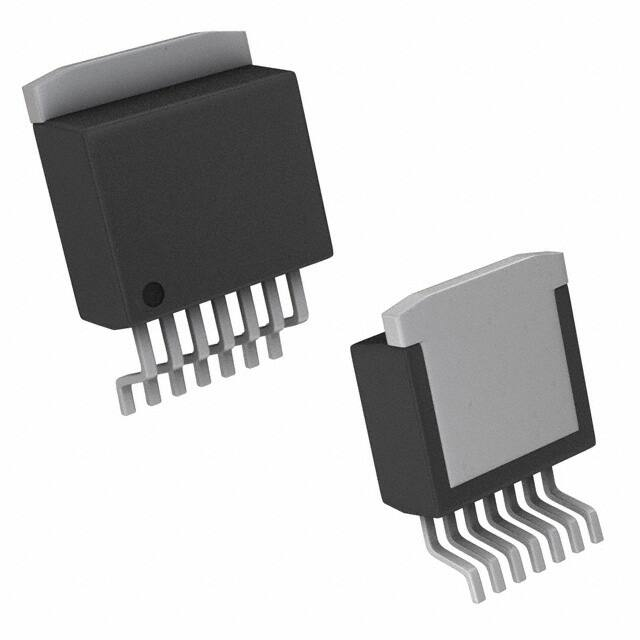
Figure 3. 7-Lead TO-263 (S)
Top View
Figure 4. 7-Lead TO-263 (S)
Side View
These devices have limited built-in ESD protection. The leads should be shorted together or the device placed in conductive foam
during storage or handling to prevent electrostatic damage to the MOS gates.
Absolute Maximum Ratings
(1)
−0.4V ≤ VIN ≤ 45V
Input Voltage
−0.4V ≤ VSW ≤ 65V
Switch Voltage
Switch Current
(2)
Internally Limited
Compensation Pin Voltage
−0.4V ≤ VCOMP ≤ 2.4V
Feedback Pin Voltage
−0.4V ≤ VFB ≤ 2 VOUT
−0.4V ≤ VSH ≤ 6V
ON /OFF Pin Voltage
−0.4V ≤ VSYNC ≤ 2V
Sync Pin Voltage
Power Dissipation
(3)
Internally Limited
−65°C to +150°C
Storage Temperature Range
Lead Temperature (Soldering, 10 sec.)
Maximum Junction Temperature
260°C
(3)
150°C
Minimum ESD Rating
(C = 100 pF, R = 1.5 kΩ)
(1)
(2)
(3)
2 kV
Absolute Maximum Ratings indicate limits beyond which damage to the device may occur. These ratings apply when the current is
limited to less than 1.2 mA for pins 1, 2, 3, and 6. Operating ratings indicate conditions for which the device is intended to be functional,
but device parameter specifications may not be guaranteed under these conditions. For guaranteed specifications and test conditions,
see the Electrical Characteristics.
Note that switch current and output current are not identical in a step-up regulator. Output current cannot be internally limited when the
LM2586 is used as a step-up regulator. To prevent damage to the switch, the output current must be externally limited to 3A. However,
output current is internally limited when the LM2586 is used as a flyback regulator (see the Application Hints section for more
information).
The junction temperature of the device (TJ) is a function of the ambient temperature (TA), the junction-to-ambient thermal resistance
(θJA), and the power dissipation of the device (PD). A thermal shutdown will occur if the temperature exceeds the maximum junction
temperature of the device: PD × θJA + TA(MAX) ≥ TJ(MAX). For a safe thermal design, check that the maximum power dissipated by the
device is less than: PD ≤ [TJ(MAX) − TA(MAX)]/θJA. When calculating the maximum allowable power dissipation, derate the maximum
junction temperature—this ensures a margin of safety in the thermal design.
Operating Ratings
4V ≤ VIN ≤ 40V
Supply Voltage
Output Switch Voltage
0V ≤ VSW ≤ 60V
Output Switch Current
ISW ≤ 3.0A
2
Submit Documentation Feedback
Copyright © 2004–2005, Texas Instruments Incorporated
Product Folder Links: LM2586
�LM2586
www.ti.com
SNVS121C – MAY 2004 – REVISED JULY 2005
Operating Ratings (continued)
−40°C ≤ TJ ≤ +125°C
Junction Temp. Range
Submit Documentation Feedback
Copyright © 2004–2005, Texas Instruments Incorporated
Product Folder Links: LM2586
3
�LM2586
SNVS121C – MAY 2004 – REVISED JULY 2005
www.ti.com
Electrical Characteristics LM2586-3.3
Specifications with standard type face are for TJ = 25°C, and those in bold type face apply over full Operating Temperature
Range. Unless otherwise specified, VIN = 5V.
Symbol
Parameters
Conditions
SYSTEM PARAMETERS Test Circuit of Figure 5
VOUT
Output Voltage
Typical
Min
Max
Units
3.3
3.17/3.14
3.43/3.46
V
20
50/100
mV
20
50/100
mV
(1)
VIN = 4V to 12V
ILOAD = 0.3 to 1.2A
ΔVOUT/
Line Regulation
VIN = 4V to 12V
ΔVIN
ΔVOUT/
ILOAD = 0.3A
Load Regulation
VIN = 12V
ΔILOAD
η
ILOAD = 0.3A to 1.2A
Efficiency
VIN = 5V, ILOAD = 0.3A
76
Output Reference
Measured at Feedback Pin
3.3
Voltage
VCOMP = 1.0V
Reference Voltage
VIN = 4V to 40V
UNIQUE DEVICE PARAMETERS
VREF
ΔVREF
%
(2)
3.242/3.234
3.358/3.366
2.0
V
mV
Line Regulation
GM
AVOL
(1)
(2)
(3)
4
Error Amp
ICOMP = −30 μA to +30 μA
Transconductance
VCOMP = 1.0V
Error Amp
VCOMP = 0.5V to 1.6V
Voltage Gain
RCOMP = 1.0 MΩ
1.193
0.678
260
151/75
2.259
mmho
V/V
(3)
External components such as the diode, inductor, input and output capacitors can affect switching regulator performance. When the
LM2586 is used as shown in Figure 5 Figure 6, system performance will be as specified by the system parameters.
All room temperature limits are 100% production tested, and all limits at temperature extremes are guaranteed via correlation using
standard Statistical Quality Control (SQC) methods.
A 1.0 MΩ resistor is connected to the compensation pin (which is the error amplifier output) to ensure accuracy in measuring AVOL.
Submit Documentation Feedback
Copyright © 2004–2005, Texas Instruments Incorporated
Product Folder Links: LM2586
�LM2586
www.ti.com
SNVS121C – MAY 2004 – REVISED JULY 2005
LM2586-5.0
Symbol
Parameters
Conditions
SYSTEM PARAMETERS Test Circuit of Figure 5
VOUT
Output Voltage
Typical
Min
Max
Units
5.0
4.80/4.75
5.20/5.25
V
20
50/100
mV
20
50/100
mV
(1)
VIN = 4V to 12V
ILOAD = 0.3A to 1.1A
ΔVOUT/
Line Regulation
VIN = 4V to 12V
ΔVIN
ΔVOUT/
ILOAD = 0.3A
Load Regulation
VIN = 12V
ΔILOAD
η
ILOAD = 0.3A to 1.1A
Efficiency
UNIQUE DEVICE PARAMETERS
VIN = 12V, ILOAD = 0.6A
80
%
(2)
VREF
Output Reference
Voltage
Measured at Feedback Pin
VCOMP = 1.0V
5.0
ΔVREF
Reference Voltage
VIN = 4V to 40V
3.3
4.913/4.900
5.088/5.100
V
mV
Line Regulation
GM
AVOL
Error Amp
ICOMP = −30 μA to +30 μA
Transconductance
VCOMP = 1.0V
Error Amp
VCOMP = 0.5V to 1.6V
Voltage Gain
(1)
(2)
(3)
RCOMP = 1.0 MΩ
0.750
0.447
165
99/49
1.491
mmho
V/V
(3)
External components such as the diode, inductor, input and output capacitors can affect switching regulator performance. When the
LM2586 is used as shown in Figure 5 Figure 6, system performance will be as specified by the system parameters.
All room temperature limits are 100% production tested, and all limits at temperature extremes are guaranteed via correlation using
standard Statistical Quality Control (SQC) methods.
A 1.0 MΩ resistor is connected to the compensation pin (which is the error amplifier output) to ensure accuracy in measuring AVOL.
Submit Documentation Feedback
Copyright © 2004–2005, Texas Instruments Incorporated
Product Folder Links: LM2586
5
�LM2586
SNVS121C – MAY 2004 – REVISED JULY 2005
www.ti.com
LM2586-12
Symbol
Parameters
Conditions
SYSTEM PARAMETERS Test Circuit of Figure 6
VOUT
Output Voltage
Typical
Min
Max
Units
12.0
11.52/11.40
12.48/12.60
V
20
100/200
mV
20
100/200
mV
(1)
VIN = 4V to 10V
ILOAD = 0.2A to 0.8A
ΔVOUT/
Line Regulation
VIN = 4V to 10V
ΔVIN
ΔVOUT/
ILOAD = 0.2A
Load Regulation
VIN = 10V
ΔILOAD
η
ILOAD = 0.2A to 0.8A
Efficiency
UNIQUE DEVICE PARAMETERS
VREF
ΔVREF
VIN = 10V, ILOAD = 0.6A
93
%
(2)
Output Reference
Measured at Feedback Pin
Voltage
VCOMP = 1.0V
Reference Voltage
VIN = 4V to 40V
12.0
11.79/11.76
12.21/12.24
7.8
V
mV
Line Regulation
GM
AVOL
Error Amp
ICOMP = −30 μA to +30 μA
Transconductance
VCOMP = 1.0V
Error Amp
VCOMP = 0.5V to 1.6V
Voltage Gain
(1)
(2)
(3)
6
RCOMP = 1.0 MΩ
0.328
0.186
70
41/21
0.621
mmho
V/V
(3)
External components such as the diode, inductor, input and output capacitors can affect switching regulator performance. When the
LM2586 is used as shown in Figure 5 Figure 6, system performance will be as specified by the system parameters.
All room temperature limits are 100% production tested, and all limits at temperature extremes are guaranteed via correlation using
standard Statistical Quality Control (SQC) methods.
A 1.0 MΩ resistor is connected to the compensation pin (which is the error amplifier output) to ensure accuracy in measuring AVOL.
Submit Documentation Feedback
Copyright © 2004–2005, Texas Instruments Incorporated
Product Folder Links: LM2586
�LM2586
www.ti.com
SNVS121C – MAY 2004 – REVISED JULY 2005
LM2586-ADJ
Symbol
Parameters
Conditions
SYSTEM PARAMETERS Test Circuit of Figure 6
VOUT
Output Voltage
Typical
Min
Max
Units
12.0
11.52/11.40
12.48/12.60
V
20
100/200
mV
20
100/200
mV
(1)
VIN = 4V to 10V
ILOAD = 0.2A to 0.8A
ΔVOUT/
Line Regulation
VIN = 4V to 10V
ΔVIN
ΔVOUT/
ILOAD = 0.2A
Load Regulation
VIN = 10V
ΔILOAD
η
ILOAD = 0.2A to 0.8A
Efficiency
UNIQUE DEVICE PARAMETERS
VREF
ΔVREF
VIN = 10V, ILOAD = 0.6A
93
%
(2)
Output Reference
Measured at Feedback Pin
Voltage
VCOMP = 1.0V
Reference Voltage
VIN = 4V to 40V
1.230
1.208/1.205
1.252/1.255
V
1.5
mV
Line Regulation
Error Amp
ICOMP = −30 μA to +30 μA
Transconductance
VCOMP = 1.0V
AVOL
Error Amp Voltage Gain
IB
Error Amp
GM
3.200
1.800
6.000
mmho
VCOMP = 0.5V to 1.6V,
RCOMP = 1.0 MΩ (3)
670
400/200
VCOMP = 1.0V
125
425/600
nA
V/V
Input Bias Current
COMMON DEVICE PARAMETERS for all versions
IS
Input Supply Current
IS/D
Shutdown Input
(2)
Switch Off
(4)
11
15.5/16.5
mA
ISWITCH = 1.8A
50
100/115
mA
VSH = 3V
16
100/300
μA
Supply Current
VUV
Input Supply
RLOAD = 100Ω
3.30
3.05
3.75
V
100
85/75
115/125
kHz
Undervoltage Lockout
fO
Oscillator Frequency
Measured at Switch Pin
RLOAD = 100Ω, VCOMP = 1.0V
Freq. Adj. Pin Open (Pin 1)
RSET = 22 kΩ
fSC
Short-Circuit
Measured at Switch Pin
Frequency
RLOAD = 100Ω
200
kHz
25
kHz
VFEEDBACK = 1.15V
VEAO
Error Amplifier
Output Swing
Upper Limit
2.8
2.6/2.4
V
(5)
Lower Limit
0.25
0.40/0.55
V
260/320
μA
(4)
IEAO
Error Amp
(6)
Output Current
165
110/70
(Source or Sink)
(1)
(2)
(3)
(4)
(5)
(6)
External components such as the diode, inductor, input and output capacitors can affect switching regulator performance. When the
LM2586 is used as shown in Figure 5 Figure 6, system performance will be as specified by the system parameters.
All room temperature limits are 100% production tested, and all limits at temperature extremes are guaranteed via correlation using
standard Statistical Quality Control (SQC) methods.
A 1.0 MΩ resistor is connected to the compensation pin (which is the error amplifier output) to ensure accuracy in measuring AVOL.
To measure this parameter, the feedback voltage is set to a high value, depending on the output version of the device, to force the error
amplifier output low and the switch off.
To measure this parameter, the feedback voltage is set to a low value, depending on the output version of the device, to force the error
amplifier output high and the switch on.
To measure the worst-case error amplifier output current, the LM2586 is tested with the feedback voltage set to its low value () and at its
high value ().
Submit Documentation Feedback
Copyright © 2004–2005, Texas Instruments Incorporated
Product Folder Links: LM2586
7
�LM2586
SNVS121C – MAY 2004 – REVISED JULY 2005
www.ti.com
LM2586-ADJ (continued)
Symbol
ISS
Parameters
Soft Start Current
Conditions
Typical
Min
Max
Units
11.0
8.0/7.0
17.0/19.0
μA
98
93/90
VFEEDBACK = 0.92V
VCOMP = 1.0V
DMAX
Maximum Duty Cycle
RLOAD = 100Ω
%
(5)
IL
Switch Leakage
Switch Off
Current
VSWITCH = 60V
VSUS
Switch Sustaining Voltage
dV/dT = 1.5V/ns
VSAT
Switch Saturation Voltage
ISWITCH = 3.0A
ICL
NPN Switch Current Limit
VSTH
Synchronization
FSYNC = 200 kHz
Threshold Voltage
VCOMP = 1V, VIN = 5V
Synchronization
VIN = 5V
Pin Current
VCOMP = 1V, VSYNC = VSTH
ON/OFF Pin (Pin 1)
VCOMP = 1V
ISYNC
VSHTH
Threshold Voltage
ISH
15
65
0.45
μA
V
0.65/0.9
V
4.0
3.0
7.0
A
0.75
0.625/0.40
0.875/1.00
V
200
μA
100
1.6
1.0/0.8
2.2/2.4
V
40
15/10
65/75
μA
(7)
ON/OFF Pin (Pin 1)
VCOMP = 1V
Current
VSH = VSHTH
Thermal Resistance
T Package, Junction to Ambient
(8)
65
θJA
T Package, Junction to Ambient
(9)
45
θJC
T Package, Junction to Case
2
θJA
S Package, Junction to Ambient
56
θJA
S Package, Junction to Ambient
35
θJA
S Package, Junction to Ambient
26
θJC
S Package, Junction to Case
2
θJA
300/600
(10)
°C/W
(11)
(12)
(7)
When testing the minimum value, do not sink current from this pin—isolate it with a diode. If current is drawn from this pin, the frequency
adjust circuit will begin operation (see Figure 40).
(8) Junction to ambient thermal resistance (no external heat sink) for the 7 lead TO-220 package mounted vertically, with ½ inch leads in a
socket, or on a PC board with minimum copper area.
(9) Junction to ambient thermal resistance (no external heat sink) for the 7 lead TO-220 package mounted vertically, with ½ inch leads
soldered to a PC board containing approximately 4 square inches of (1 oz.) copper area surrounding the leads.
(10) Junction to ambient thermal resistance for the 7 lead TO-263 mounted horizontally against a PC board area of 0.136 square inches (the
same size as the TO-263 package) of 1 oz. (0.0014 in. thick) copper.
(11) Junction to ambient thermal resistance for the 7 lead TO-263 mounted horizontally against a PC board area of 0.4896 square inches
(3.6 times the area of the TO-263 package) of 1 oz. (0.0014 in. thick) copper.
(12) Junction to ambient thermal resistance for the 7 lead TO-263 mounted horizontally against a PC board copper area of 1.0064 square
inches (7.4 times the area of the TO-263 package) of 1 oz. (0.0014 in. thick) copper. Additional copper area will reduce thermal
resistance further. See the thermal model in Switchers Made Simple® software.
8
Submit Documentation Feedback
Copyright © 2004–2005, Texas Instruments Incorporated
Product Folder Links: LM2586
�LM2586
www.ti.com
SNVS121C – MAY 2004 – REVISED JULY 2005
Typical Performance Characteristics
Supply Current
vs Temperature
Reference Voltage
vs Temperature
ΔReference Voltage
vs Supply Voltage
Supply Current
vs Switch Current
Current Limit
vs Temperature
Feedback Pin Bias
Current
vs
Temperature
Switch Saturation
Voltage
vs
Temperature
Switch Transconductance
vs Temperature
Oscillator Frequency
vs Temperature
Error Amp Transconductance
vs Temperature
Submit Documentation Feedback
Copyright © 2004–2005, Texas Instruments Incorporated
Product Folder Links: LM2586
9
�LM2586
SNVS121C – MAY 2004 – REVISED JULY 2005
www.ti.com
Typical Performance Characteristics (continued)
Error Amp Voltage
Gain
vs
Temperature
Short Circuit Frequency
vs Temperature
Shutdown Supply Current
vs Temperature
ON/OFF Pin Current
vs Voltage
Oscillator Frequency
vs Resistance
Flyback Regulator
10
Submit Documentation Feedback
Copyright © 2004–2005, Texas Instruments Incorporated
Product Folder Links: LM2586
�LM2586
www.ti.com
SNVS121C – MAY 2004 – REVISED JULY 2005
Test Circuits
CIN1—100 μF, 25V Aluminum Electrolytic
CIN2—0.1 μF Ceramic
T—22 μH, 1:1 Schott #67141450
D—1N5820
COUT—680 μF, 16V Aluminum Electrolytic
CC—0.47 μF Ceramic
RC—2k
Figure 5. LM2586-3.3 and LM2586-5.0
CIN1—100 μF, 25V Aluminum Electrolytic
CIN2—0.1 μF Ceramic
L—15 μH, Renco #RL-5472-5
D—1N5820
COUT—680 μF, 16V Aluminum Electrolytic
CC—0.47 μF Ceramic
RC—2k
For 12V Devices: R1 = Short (0Ω) and 2 = Open
For ADJ Devices: R1 = 48.75k, ±0.1% and 2 = 5.62k, ±0.1%
Figure 6. LM2586-12 and LM2586-ADJ
Submit Documentation Feedback
Copyright © 2004–2005, Texas Instruments Incorporated
Product Folder Links: LM2586
11
�LM2586
SNVS121C – MAY 2004 – REVISED JULY 2005
www.ti.com
Block Diagram
For Fixed Versions
3.3V, R1 = 3.4k, R2 = 2k
5.0V, R1 = 6.15k, R2 = 2k
12V, R1 = 8.73k, R2 = 1k
For Adj. Version
R1 = Short (0Ω), R2 = Open
Flyback Regulator Operation
The LM2586 is ideally suited for use in the flyback regulator topology. The flyback regulator can produce a single
output voltage, such as the one shown in Figure 7, or multiple output voltages. In Figure 7, the flyback regulator
generates an output voltage that is inside the range of the input voltage. This feature is unique to flyback
regulators and cannot be duplicated with buck or boost regulators.
The operation of a flyback regulator is as follows (refer to Figure 7): when the switch is on, current flows through
the primary winding of the transformer, T1, storing energy in the magnetic field of the transformer. Note that the
primary and secondary windings are out of phase, so no current flows through the secondary when current flows
through the primary. When the switch turns off, the magnetic field collapses, reversing the voltage polarity of the
primary and secondary windings. Now rectifier D1 is forward biased and current flows through it, releasing the
energy stored in the transformer. This produces voltage at the output.
The output voltage is controlled by modulating the peak switch current. This is done by feeding back a portion of
the output voltage to the error amp, which amplifies the difference between the feedback voltage and a 1.230V
reference. The error amp output voltage is compared to a ramp voltage proportional to the switch current (i.e.,
inductor current during the switch on time). The comparator terminates the switch on time when the two voltages
are equal, thereby controlling the peak switch current to maintain a constant output voltage.
12
Submit Documentation Feedback
Copyright © 2004–2005, Texas Instruments Incorporated
Product Folder Links: LM2586
�LM2586
www.ti.com
SNVS121C – MAY 2004 – REVISED JULY 2005
As shown in Figure 7, the LM2586 can be used as a flyback regulator by using a minimum number of external
components. The switching waveforms of this regulator are shown in Figure 8. Typical Performance Characteristics
observed during the operation of this circuit are shown in Figure 9.
Figure 7. 12V Flyback Regulator Design Example
Submit Documentation Feedback
Copyright © 2004–2005, Texas Instruments Incorporated
Product Folder Links: LM2586
13
�LM2586
SNVS121C – MAY 2004 – REVISED JULY 2005
www.ti.com
Typical Performance Characteristics
A: Switch Voltage, 20V/div
B: Switch Current, 2A/div
C: Output Rectifier Current, 2A/div
D: Output Ripple Voltage, 50 mV/div AC-Coupled
Figure 8. Switching Waveforms
Figure 9. VOUT Response to Load Current Step
Typical Flyback Regulator Applications
Figure 10 through Figure 15 show six typical flyback applications, varying from single output to triple output. Each
drawing contains the part number(s) and manufacturer(s) for every component except the transformer. For the
transformer part numbers and manufacturers' names, see the table in Table 1. For applications with different
output voltages—requiring the LM2586-ADJ—or different output configurations that do not match the standard
configurations, refer to the Switchers Made Simple software.
Figure 10. Single-Output Flyback Regulator
14
Submit Documentation Feedback
Copyright © 2004–2005, Texas Instruments Incorporated
Product Folder Links: LM2586
�LM2586
www.ti.com
SNVS121C – MAY 2004 – REVISED JULY 2005
Figure 11. Single-Output Flyback Regulator
Figure 12. Single-Output Flyback Regulator
Submit Documentation Feedback
Copyright © 2004–2005, Texas Instruments Incorporated
Product Folder Links: LM2586
15
�LM2586
SNVS121C – MAY 2004 – REVISED JULY 2005
www.ti.com
Figure 13. Dual-Output Flyback Regulator
Figure 14. Dual-Output Flyback Regulator
16
Submit Documentation Feedback
Copyright © 2004–2005, Texas Instruments Incorporated
Product Folder Links: LM2586
�LM2586
www.ti.com
SNVS121C – MAY 2004 – REVISED JULY 2005
Figure 15. Triple-Output Flyback Regulator
TRANSFORMER SELECTION (T)
Table 1 lists the standard transformers available for flyback regulator applications. Included in the table are the
turns ratio(s) for each transformer, as well as the output voltages, input voltage ranges, and the maximum load
currents for each circuit.
Table 1. Transformer Selection Table
Applications
Figure 10
Figure 11
Figure 12
Figure 13
Figure 14
Transformers
T7
T7
T7
T6
T6
T5
4V–6V
4V–6V
8V–16V
4V–6V
18V–36V
18V–36V
VOUT1
3.3V
5V
12V
12V
12V
5V
IOUT1 (Max)
1.4A
1A
0.8A
0.15A
0.6A
1.8A
1
1
1
1.2
1.2
0.5
VOUT2
−12V
−12V
12V
IOUT2(Max)
0.15A
0.6A
0.25A
1.2
1.2
VIN
N1
N2
Figure 15
1.15
VOUT3
−12V
IOUT3 (Max)
0.25A
N3
1.15
Submit Documentation Feedback
Copyright © 2004–2005, Texas Instruments Incorporated
Product Folder Links: LM2586
17
�LM2586
SNVS121C – MAY 2004 – REVISED JULY 2005
www.ti.com
Table 2. Transformer Manufacturer Guide
Transformer
Type
Manufacturers' Part Numbers
Coilcraft
(1)
(2)
(3)
(4)
Coilcraft (1) Surface
Mount
(1)
Pulse (2) Surface
Mount
Pulse
(2)
Renco
(3)
Schott
(4)
T5
Q4338-B
Q4437-B
PE-68413
—
RL-5532
67140890
T6
Q4339-B
Q4438-B
PE-68414
—
RL-5533
67140900
T7
S6000-A
S6057-A
—
PE-68482
RL-5751
26606
Coilcraft Inc., Phone: (800) 322-26451102 Silver Lake Road, Cary, IL 60013 Fax: (708) 639-1469 European Headquarters, 21
Napier Place Phone: +44 1236 730 595Wardpark North, Cumbernauld, Scotland G68 0LL Fax: +44 1236 730 627
Pulse Engineering Inc., Phone: (619) 674-810012220 World Trade Drive, San Diego, CA 92128 Fax: (619) 674-8262European
Headquarters, Dunmore Road Phone: +353 93 24 107Tuam, Co. Galway, Ireland Fax: +353 93 24 459
Renco Electronics Inc., Phone: (800) 645-582860 Jeffryn Blvd. East, Deer Park, NY 11729 Fax: (516) 586-5562
Schott Corp., Phone: (612) 475-11731000 Parkers Lane Road, Wayzata, MN 55391 Fax: (612) 475-1786
TRANSFORMER FOOTPRINTS
Figure 16 through Figure 30 show the footprints of each transformer, listed in Table 2.
T7
T6
Figure 16. Coilcraft S6000-A (Top View)
Figure 17. Coilcraft Q4339-B (Top View)
T5
T5
Figure 18. Coilcraft Q4437-B (Surface Mount) (Top
View)
Figure 19. Coilcraft Q4338-B (Top View)
T7
T6
Figure 20. Coilcraft S6057-A
(Surface Mount) (Top View)
18
Figure 21. Coilcraft Q4438-B
(Surface Mount) (Top View)
Submit Documentation Feedback
Copyright © 2004–2005, Texas Instruments Incorporated
Product Folder Links: LM2586
�LM2586
www.ti.com
SNVS121C – MAY 2004 – REVISED JULY 2005
T7
T6
Figure 22. Pulse PE-68482 (Top View)
Figure 23. Pulse PE-68414
(Surface Mount) (Top View)
T5
T7
Figure 24. Pulse PE-68413
(Surface Mount) (Top View)
Figure 25. Renco RL-5751 (Top View)
T6
T5
Figure 26. Renco RL-5533 (Top View)
Figure 27. Renco RL-5532 (Top View)
T7
T6
Figure 28. Schott 26606 (Top View)
Figure 29. Schott 67140900 (Top View)
T5
Figure 30. Schott 67140890 (Top View)
Submit Documentation Feedback
Copyright © 2004–2005, Texas Instruments Incorporated
Product Folder Links: LM2586
19
�LM2586
SNVS121C – MAY 2004 – REVISED JULY 2005
www.ti.com
Step-Up (Boost) Regulator Operation
Figure 31 shows the LM2586 used as a step-up (boost) regulator. This is a switching regulator that produces an
output voltage greater than the input supply voltage.
A brief explanation of how the LM2586 Boost Regulator works is as follows (refer to Figure 31). When the NPN
switch turns on, the inductor current ramps up at the rate of VIN/L, storing energy in the inductor. When the
switch turns off, the lower end of the inductor flies above VIN, discharging its current through diode (D) into the
output capacitor (COUT) at a rate of (VOUT − VIN)/L. Thus, energy stored in the inductor during the switch on time
is transferred to the output during the switch off time. The output voltage is controlled by adjusting the peak
switch current, as described in the flyback regulator section.
Figure 31. 12V Boost Regulator
By adding a small number of external components (as shown in Figure 31), the LM2586 can be used to produce
a regulated output voltage that is greater than the applied input voltage. The switching waveforms observed
during the operation of this circuit are shown in Figure 32. Typical performance of this regulator is shown in
Figure 33.
20
Submit Documentation Feedback
Copyright © 2004–2005, Texas Instruments Incorporated
Product Folder Links: LM2586
�LM2586
www.ti.com
SNVS121C – MAY 2004 – REVISED JULY 2005
Typical Performance Characteristics
A: Switch Voltage,10V/div
B: Switch Current, 2A/div
C: Inductor Current, 2A/div
D: Output Ripple Voltage,100 mV/div, AC-Coupled
Figure 32. Switching Waveforms
Figure 33. VOUT Response to Load Current Step
Typical Boost Regulator Applications
Figure 34 Figure 35 through Figure 37 show four typical boost applications—one fixed and three using the
adjustable version of the LM2586. Each drawing contains the part number(s) and manufacturer(s) for every
component. For the fixed 12V output application, the part numbers and manufacturers' names for the inductor
are listed in a table in Table 3. For applications with different output voltages, refer to the Switchers Made
Simple software.
Figure 34. +5V to +12V Boost Regulator
Table 3 contains a table of standard inductors, by part number and corresponding manufacturer, for the fixed
output regulator of Figure 34.
Submit Documentation Feedback
Copyright © 2004–2005, Texas Instruments Incorporated
Product Folder Links: LM2586
21
�LM2586
SNVS121C – MAY 2004 – REVISED JULY 2005
www.ti.com
Table 3. Inductor Selection Table
Coilcraft
Pulse
(1)
Renco
(2)
Schott
(3)
(4)
Schott
(4)
(Surface Mount)
DO3316-153
(1)
(2)
(3)
(4)
PE-53898
RL-5471-7
67146510
67146540
Coilcraft Inc., Phone: (800) 322-26451102 Silver Lake Road, Cary, IL 60013 Fax: (708) 639-1469European Headquarters, 21 Napier
Place Phone: +44 1236 730 595Wardpark North, Cumbernauld, Scotland G68 0LL Fax: +44 1236 730 627
Pulse Engineering Inc., Phone: (619) 674-810012220 World Trade Drive, San Diego, CA 92128 Fax: (619) 674-8262European
Headquarters, Dunmore Road Phone: +353 93 24 107Tuam, Co. Galway, Ireland Fax: +353 93 24 459
Renco Electronics Inc., Phone: (800) 645-582860 Jeffryn Blvd. East, Deer Park, NY 11729 Fax: (516) 586-5562
Schott Corp., Phone: (612) 475-11731000 Parkers Lane Road, Wayzata, MN 55391 Fax: (612) 475-1786
Figure 35. +12V to +24V Boost Regulator
(1)
Figure 36. +24V to +36V Boost Regulator
The LM2586 will require a heat sink in these applications. The size of the heat sink will depend on the maximum
ambient temperature. To calculate the thermal resistance of the IC and the size of the heat sink needed, see the
“Heat Sink/Thermal Considerations” section in the Application Hints.
Figure 37. +24V to +48V Boost Regulator
Application Hints
LM2586 SPECIAL FEATURES
Figure 38. Shutdown Operation
22
Submit Documentation Feedback
Copyright © 2004–2005, Texas Instruments Incorporated
Product Folder Links: LM2586
�LM2586
www.ti.com
SNVS121C – MAY 2004 – REVISED JULY 2005
SHUTDOWN CONTROL
A feature of the LM2586 is its ability to be shut down using the ON /OFF pin (pin 1). This feature conserves input
power by turning off the device when it is not in use. For proper operation, an isolation diode is required (as
shown in Figure 38).
The device will shut down when 3V or greater is applied on the ON /OFF pin, sourcing current into pin 1. In shut
down mode, the device will draw typically 56 μA of supply current (16 μA to VIN and 40 μA to the ON /OFF pin).
To turn the device back on, leave pin 1 floating, using an (isolation) diode, as shown in Figure 38 (for normal
operation, do not source or sink current to or from this pin—see the next section).
FREQUENCY ADJUSTMENT
The switching frequency of the LM2586 can be adjusted with the use of an external resistor. This feature allows
the user to optimize the size of the magnetics and the output capacitor(s) by tailoring the operating frequency. A
resistor connected from pin 1 (the Freq. Adj. pin) to ground will set the switching frequency from 100 kHz to 200
kHz (maximum). As shown in Figure 38, the pin can be used to adjust the frequency while still providing the shut
down function. A curve in the Performance Characteristics Section graphs the resistor value to the corresponding
switching frequency. The table in Table 4 shows resistor values corresponding to commonly used frequencies.
However, changing the LM2586's operating frequency from its nominal value of 100 kHz will change the
magnetics selection and compensation component values.
Table 4. Frequency Setting Resistor Guide
RSET(kΩ)
Frequency (kHz)
Open
100
200
125
47
150
33
175
22
200
Figure 39. Frequency Synchronization
FREQUENCY SYNCHRONIZATION
Another feature of the LM2586 is the ability to synchronize the switching frequency to an external source, using
the sync pin (pin 6). This feature allows the user to parallel multiple devices to deliver more output power.
A negative falling pulse applied to the sync pin will synchronize the LM2586 to an external oscillator (see
Figure 39 Figure 40).
Use of this feature enables the LM2586 to be synchronized to an external oscillator, such as a system clock. This
operation allows multiple power supplies to operate at the same frequency, thus eliminating frequency-related
noise problems.
Submit Documentation Feedback
Copyright © 2004–2005, Texas Instruments Incorporated
Product Folder Links: LM2586
23
�LM2586
SNVS121C – MAY 2004 – REVISED JULY 2005
www.ti.com
Figure 40. Waveforms of a Synchronized 12V Boost Regulator
The scope photo in Figure 40 shows a LM2586 12V Boost Regulator synchronized to a 200 kHz signal. There is
a 700 ns delay between the falling edge of the sync signal and the turning on of the switch.
Figure 41. Boost Regulator
PROGRAMMING OUTPUT VOLTAGE (SELECTING R1 AND R2)
Referring to the adjustable regulator in Figure 41, the output voltage is programmed by the resistors R1 and R2
by the following formula:
VOUT = VREF (1 + R1/R2)
where VREF = 1.23V
(1)
Resistors R1 and R2 divide the output voltage down so that it can be compared with the 1.23V internal
reference. With R2 between 1k and 5k, R1 is:
R1 = R2 (VOUT/VREF − 1)
where VREF = 1.23V
(2)
For best temperature coefficient and stability with time, use 1% metal film resistors.
24
Submit Documentation Feedback
Copyright © 2004–2005, Texas Instruments Incorporated
Product Folder Links: LM2586
�LM2586
www.ti.com
SNVS121C – MAY 2004 – REVISED JULY 2005
SHORT CIRCUIT CONDITION
Due to the inherent nature of boost regulators, when the output is shorted (see Figure 41), current flows directly
from the input, through the inductor and the diode, to the output, bypassing the switch. The current limit of the
switch does not limit the output current for the entire circuit. To protect the load and prevent damage to the
switch, the current must be externally limited, either by the input supply or at the output with an external current
limit circuit. The external limit should be set to the maximum switch current of the device, which is 3A.
In a flyback regulator application (Figure 42), using the standard transformers, the LM2586 will survive a short
circuit to the main output. When the output voltage drops to 80% of its nominal value, the frequency will drop to
25 kHz. With a lower frequency, off times are larger. With the longer off times, the transformer can release all of
its stored energy before the switch turns back on. Hence, the switch turns on initially with zero current at its
collector. In this condition, the switch current limit will limit the peak current, saving the device.
FLYBACK REGULATOR INPUT CAPACITORS
A flyback regulator draws discontinuous pulses of current from the input supply. Therefore, there are two input
capacitors needed in a flyback regulator—one for energy storage and one for filtering (see Figure 42). Both are
required due to the inherent operation of a flyback regulator. To keep a stable or constant voltage supply to the
LM2586, a storage capacitor (≥100 μF) is required. If the input source is a rectified DC supply and/or the
application has a wide temperature range, the required rms current rating of the capacitor might be very large.
This means a larger value of capacitance or a higher voltage rating will be needed for the input capacitor. The
storage capacitor will also attenuate noise which may interfere with other circuits connected to the same input
supply voltage.
Figure 42. Flyback Regulator
In addition, a small bypass capacitor is required due to the noise generated by the input current pulses. To
eliminate the noise, insert a 1.0 μF ceramic capacitor between VIN and ground as close as possible to the device.
SWITCH VOLTAGE LIMITS
In a flyback regulator, the maximum steady-state voltage appearing at the switch, when it is off, is set by the
transformer turns ratio, N, the output voltage, VOUT, and the maximum input voltage, VIN (Max):
VSW(OFF) = VIN (Max) + (VOUT +VF)/N
(3)
Submit Documentation Feedback
Copyright © 2004–2005, Texas Instruments Incorporated
Product Folder Links: LM2586
25
�LM2586
SNVS121C – MAY 2004 – REVISED JULY 2005
www.ti.com
where VF is the forward biased voltage of the output diode, and is typically 0.5V for Schottky diodes and 0.8V for
ultra-fast recovery diodes. In certain circuits, there exists a voltage spike, VLL, superimposed on top of the
steady-state voltage (see Figure 8, waveform A). Usually, this voltage spike is caused by the transformer leakage
inductance and/or the output rectifier recovery time. To “clamp” the voltage at the switch from exceeding its
maximum value, a transient suppressor in series with a diode is inserted across the transformer primary (as
shown in the circuit in Figure 7 and other flyback regulator circuits throughout the datasheet). The schematic in
Figure 42 shows another method of clamping the switch voltage. A single voltage transient suppressor (the
SA51A) is inserted at the switch pin. This method clamps the total voltage across the switch, not just the voltage
across the primary.
If poor circuit layout techniques are used (see the “Circuit Layout Guideline” section), negative voltage transients
may appear on the Switch pin (pin 5). Applying a negative voltage (with respect to the IC's ground) to any
monolithic IC pin causes erratic and unpredictable operation of that IC. This holds true for the LM2586 IC as well.
When used in a flyback regulator, the voltage at the Switch pin (pin 5) can go negative when the switch turns on.
The “ringing” voltage at the switch pin is caused by the output diode capacitance and the transformer leakage
inductance forming a resonant circuit at the secondary(ies). The resonant circuit generates the “ringing” voltage,
which gets reflected back through the transformer to the switch pin. There are two common methods to avoid this
problem. One is to add an RC snubber around the output rectifier(s), as in Figure 42. The values of the resistor
and the capacitor must be chosen so that the voltage at the Switch pin does not drop below −0.4V. The resistor
may range in value between 10Ω and 1 kΩ, and the capacitor will vary from 0.001 μF to 0.1 μF. Adding a
snubber will (slightly) reduce the efficiency of the overall circuit.
The other method to reduce or eliminate the “ringing” is to insert a Schottky diode clamp between pins 5 and 4
(ground), also shown in Figure 42. This prevents the voltage at pin 5 from dropping below −0.4V. The reverse
voltage rating of the diode must be greater than the switch off voltage.
Figure 43. Input Line Filter
OUTPUT VOLTAGE LIMITATIONS
The maximum output voltage of a boost regulator is the maximum switch voltage minus a diode drop. In a
flyback regulator, the maximum output voltage is determined by the turns ratio, N, and the duty cycle, D, by the
equation:
VOUT ≈ N × VIN × D/(1 − D)
(4)
The duty cycle of a flyback regulator is determined by the following equation:
(5)
Theoretically, the maximum output voltage can be as large as desired—just keep increasing the turns ratio of the
transformer. However, there exists some physical limitations that prevent the turns ratio, and thus the output
voltage, from increasing to infinity. The physical limitations are capacitances and inductances in the LM2586
switch, the output diode(s), and the transformer—such as reverse recovery time of the output diode (mentioned
above).
26
Submit Documentation Feedback
Copyright © 2004–2005, Texas Instruments Incorporated
Product Folder Links: LM2586
�LM2586
www.ti.com
SNVS121C – MAY 2004 – REVISED JULY 2005
NOISY INPUT LINE CONDITION
A small, low-pass RC filter should be used at the input pin of the LM2586 if the input voltage has an unusually
large amount of transient noise, such as with an input switch that bounces. The circuit in Figure 43 demonstrates
the layout of the filter, with the capacitor placed from the input pin to ground and the resistor placed between the
input supply and the input pin. Note that the values of RIN and CIN shown in the schematic are good enough for
most applications, but some readjusting might be required for a particular application. If efficiency is a major
concern, replace the resistor with a small inductor (say 10 μH and rated at 200 mA).
STABILITY
All current-mode controlled regulators can suffer from an instability, known as subharmonic oscillation, if they
operate with a duty cycle above 50%. To eliminate subharmonic oscillations, a minimum value of inductance is
required to ensure stability for all boost and flyback regulators. The minimum inductance is given by:
(6)
where VSAT is the switch saturation voltage and can be found in the Characteristic Curves.
Figure 44. Circuit Board Layout
CIRCUIT LAYOUT GUIDELINES
As in any switching regulator, layout is very important. Rapidly switching currents associated with wiring
inductance generate voltage transients which can cause problems. For minimal inductance and ground loops,
keep the length of the leads and traces as short as possible. Use single point grounding or ground plane
construction for best results. Separate the signal grounds from the power grounds (as indicated in Figure 44).
When using the Adjustable version, physically locate the programming resistors as near the regulator IC as
possible, to keep the sensitive feedback wiring short.
HEAT SINK/THERMAL CONSIDERATIONS
In many cases, a heat sink is not required to keep the LM2586 junction temperature within the allowed operating
temperature range. For each application, to determine whether or not a heat sink will be required, the following
must be identified:
1) Maximum ambient temperature (in the application).
2) Maximum regulator power dissipation (in the application).
3) Maximum allowed junction temperature (125°C for the LM2586). For a safe, conservative design, a
temperature approximately 15°C cooler than the maximum junction temperature should be selected (110°C).
4) LM2586 package thermal resistances θJA and θJC (given in the Electrical Characteristics).
Total power dissipated (PD) by the LM2586 can be estimated as follows:
Submit Documentation Feedback
Copyright © 2004–2005, Texas Instruments Incorporated
Product Folder Links: LM2586
27
�LM2586
SNVS121C – MAY 2004 – REVISED JULY 2005
www.ti.com
(7)
VIN is the minimum input voltage, VOUT is the output voltage, N is the transformer turns ratio, D is the duty cycle,
and ILOAD is the maximum load current (and ∑ILOAD is the sum of the maximum load currents for multiple-output
flyback regulators). The duty cycle is given by:
(8)
where VF is the forward biased voltage of the diode and is typically 0.5V for Schottky diodes and 0.8V for fast
recovery diodes. VSAT is the switch saturation voltage and can be found in the Characteristic Curves.
When no heat sink is used, the junction temperature rise is:
ΔTJ = PD • θJA.
(9)
Adding the junction temperature rise to the maximum ambient temperature gives the actual operating junction
temperature:
TJ = ΔTJ + TA.
(10)
If the operating junction temperature exceeds the maximum junction temperatue in item 3 above, then a heat
sink is required. When using a heat sink, the junction temperature rise can be determined by the following:
ΔTJ = PD • (θJC + θInterface + θHeat Sink)
(11)
Again, the operating junction temperature will be:
TJ = ΔTJ + TA
(12)
As before, if the maximum junction temperature is exceeded, a larger heat sink is required (one that has a lower
thermal resistance).
Included in the Switchers Made Simple® design software is a more precise (non-linear) thermal model that can
be used to determine junction temperature with different input-output parameters or different component values.
It can also calculate the heat sink thermal resistance required to maintain the regulator junction temperature
below the maximum operating temperature.
To further simplify the flyback regulator design procedure, National Semiconductor is making available computer
design software to be used with the Simple Switcher® line of switching regulators. Switchers Made Simpleis
available on a 3½″ diskette for IBM compatible computers from a National Semiconductor sales office in your
area or the National Semiconductor Customer Response Center (1-800-272-9959).
28
Submit Documentation Feedback
Copyright © 2004–2005, Texas Instruments Incorporated
Product Folder Links: LM2586
�PACKAGE OPTION ADDENDUM
www.ti.com
17-Nov-2012
PACKAGING INFORMATION
Orderable Device
Status
(1)
Package Type Package Pins Package Qty
Drawing
Eco Plan
Lead/Ball Finish
(2)
MSL Peak Temp
Samples
(3)
(Requires Login)
LM2586S-12
ACTIVE
DDPAK
KTW
7
45
TBD
CU SNPB
Level-3-235C-168 HR
LM2586S-12/NOPB
ACTIVE
DDPAK
KTW
7
45
Pb-Free (RoHS
Exempt)
CU SN
Level-3-245C-168 HR
LM2586S-3.3
ACTIVE
DDPAK
KTW
7
45
TBD
CU SNPB
Level-3-235C-168 HR
LM2586S-3.3/NOPB
ACTIVE
DDPAK
KTW
7
45
Pb-Free (RoHS
Exempt)
CU SN
Level-3-245C-168 HR
LM2586S-5.0
ACTIVE
DDPAK
KTW
7
45
TBD
CU SNPB
Level-3-235C-168 HR
LM2586S-5.0/NOPB
ACTIVE
DDPAK
KTW
7
45
Pb-Free (RoHS
Exempt)
CU SN
Level-3-245C-168 HR
LM2586S-ADJ
ACTIVE
DDPAK
KTW
7
45
TBD
CU SNPB
Level-3-235C-168 HR
LM2586S-ADJ/NOPB
ACTIVE
DDPAK
KTW
7
45
Pb-Free (RoHS
Exempt)
CU SN
Level-3-245C-168 HR
LM2586SX-3.3
ACTIVE
DDPAK
KTW
7
500
TBD
CU SNPB
Level-3-235C-168 HR
LM2586SX-3.3/NOPB
ACTIVE
DDPAK
KTW
7
500
Pb-Free (RoHS
Exempt)
CU SN
Level-3-245C-168 HR
LM2586SX-5.0
ACTIVE
DDPAK
KTW
7
500
TBD
CU SNPB
Level-3-235C-168 HR
LM2586SX-5.0/NOPB
ACTIVE
DDPAK
KTW
7
500
Pb-Free (RoHS
Exempt)
CU SN
Level-3-245C-168 HR
LM2586SX-ADJ
ACTIVE
DDPAK
KTW
7
500
TBD
CU SNPB
Level-3-235C-168 HR
LM2586SX-ADJ/NOPB
ACTIVE
DDPAK
KTW
7
500
Pb-Free (RoHS
Exempt)
CU SN
Level-3-245C-168 HR
LM2586T-3.3
ACTIVE
TO-220
NDZ
7
45
TBD
CU SNPB
Level-1-NA-UNLIM
LM2586T-3.3/NOPB
ACTIVE
TO-220
NDZ
7
45
Pb-Free (RoHS
Exempt)
CU SN
Level-1-NA-UNLIM
LM2586T-5.0
ACTIVE
TO-220
NDZ
7
45
TBD
CU SNPB
Level-1-NA-UNLIM
LM2586T-5.0/NOPB
ACTIVE
TO-220
NDZ
7
45
Pb-Free (RoHS
Exempt)
CU SN
Level-1-NA-UNLIM
LM2586T-ADJ
ACTIVE
TO-220
NDZ
7
45
TBD
CU SNPB
Level-1-NA-UNLIM
LM2586T-ADJ/NOPB
ACTIVE
TO-220
NDZ
7
45
Pb-Free (RoHS
Exempt)
CU SN
Level-1-NA-UNLIM
(1)
The marketing status values are defined as follows:
ACTIVE: Product device recommended for new designs.
Addendum-Page 1
�PACKAGE OPTION ADDENDUM
www.ti.com
17-Nov-2012
LIFEBUY: TI has announced that the device will be discontinued, and a lifetime-buy period is in effect.
NRND: Not recommended for new designs. Device is in production to support existing customers, but TI does not recommend using this part in a new design.
PREVIEW: Device has been announced but is not in production. Samples may or may not be available.
OBSOLETE: TI has discontinued the production of the device.
(2)
Eco Plan - The planned eco-friendly classification: Pb-Free (RoHS), Pb-Free (RoHS Exempt), or Green (RoHS & no Sb/Br) - please check http://www.ti.com/productcontent for the latest availability
information and additional product content details.
TBD: The Pb-Free/Green conversion plan has not been defined.
Pb-Free (RoHS): TI's terms "Lead-Free" or "Pb-Free" mean semiconductor products that are compatible with the current RoHS requirements for all 6 substances, including the requirement that
lead not exceed 0.1% by weight in homogeneous materials. Where designed to be soldered at high temperatures, TI Pb-Free products are suitable for use in specified lead-free processes.
Pb-Free (RoHS Exempt): This component has a RoHS exemption for either 1) lead-based flip-chip solder bumps used between the die and package, or 2) lead-based die adhesive used between
the die and leadframe. The component is otherwise considered Pb-Free (RoHS compatible) as defined above.
Green (RoHS & no Sb/Br): TI defines "Green" to mean Pb-Free (RoHS compatible), and free of Bromine (Br) and Antimony (Sb) based flame retardants (Br or Sb do not exceed 0.1% by weight
in homogeneous material)
(3)
MSL, Peak Temp. -- The Moisture Sensitivity Level rating according to the JEDEC industry standard classifications, and peak solder temperature.
Important Information and Disclaimer:The information provided on this page represents TI's knowledge and belief as of the date that it is provided. TI bases its knowledge and belief on information
provided by third parties, and makes no representation or warranty as to the accuracy of such information. Efforts are underway to better integrate information from third parties. TI has taken and
continues to take reasonable steps to provide representative and accurate information but may not have conducted destructive testing or chemical analysis on incoming materials and chemicals.
TI and TI suppliers consider certain information to be proprietary, and thus CAS numbers and other limited information may not be available for release.
In no event shall TI's liability arising out of such information exceed the total purchase price of the TI part(s) at issue in this document sold by TI to Customer on an annual basis.
Addendum-Page 2
�PACKAGE MATERIALS INFORMATION
www.ti.com
17-Nov-2012
TAPE AND REEL INFORMATION
*All dimensions are nominal
Device
Package Package Pins
Type Drawing
SPQ
Reel
Reel
A0
Diameter Width (mm)
(mm) W1 (mm)
B0
(mm)
K0
(mm)
P1
(mm)
W
Pin1
(mm) Quadrant
LM2586SX-3.3
DDPAK
KTW
7
500
330.0
24.4
10.75
14.85
5.0
16.0
24.0
Q2
LM2586SX-3.3/NOPB
DDPAK
KTW
7
500
330.0
24.4
10.75
14.85
5.0
16.0
24.0
Q2
LM2586SX-5.0
DDPAK
KTW
7
500
330.0
24.4
10.75
14.85
5.0
16.0
24.0
Q2
LM2586SX-5.0/NOPB
DDPAK
KTW
7
500
330.0
24.4
10.75
14.85
5.0
16.0
24.0
Q2
LM2586SX-ADJ
DDPAK
KTW
7
500
330.0
24.4
10.75
14.85
5.0
16.0
24.0
Q2
LM2586SX-ADJ/NOPB
DDPAK
KTW
7
500
330.0
24.4
10.75
14.85
5.0
16.0
24.0
Q2
Pack Materials-Page 1
�PACKAGE MATERIALS INFORMATION
www.ti.com
17-Nov-2012
*All dimensions are nominal
Device
Package Type
Package Drawing
Pins
SPQ
Length (mm)
Width (mm)
Height (mm)
LM2586SX-3.3
DDPAK
KTW
7
500
358.0
343.0
63.0
LM2586SX-3.3/NOPB
DDPAK
KTW
7
500
358.0
343.0
63.0
LM2586SX-5.0
DDPAK
KTW
7
500
358.0
343.0
63.0
LM2586SX-5.0/NOPB
DDPAK
KTW
7
500
358.0
343.0
63.0
LM2586SX-ADJ
DDPAK
KTW
7
500
358.0
343.0
63.0
LM2586SX-ADJ/NOPB
DDPAK
KTW
7
500
358.0
343.0
63.0
Pack Materials-Page 2
�MECHANICAL DATA
NDZ0007B
TA07B (Rev E)
www.ti.com
�MECHANICAL DATA
MPSF015 – AUGUST 2001
KTW (R-PSFM-G7)
PLASTIC FLANGE-MOUNT
0.410 (10,41)
0.385 (9,78)
0.304 (7,72)
–A–
0.006
–B–
0.303 (7,70)
0.297 (7,54)
0.0625 (1,587) H
0.055 (1,40)
0.0585 (1,485)
0.300 (7,62)
0.064 (1,63)
0.045 (1,14)
0.252 (6,40)
0.056 (1,42)
0.187 (4,75)
0.370 (9,40)
0.179 (4,55)
0.330 (8,38)
H
0.296 (7,52)
A
0.605 (15,37)
0.595 (15,11)
0.012 (0,305)
C
0.000 (0,00)
0.019 (0,48)
0.104 (2,64)
0.096 (2,44)
H
0.017 (0,43)
0.050 (1,27)
C
C
F
0.034 (0,86)
0.022 (0,57)
0.010 (0,25) M
B
0.026 (0,66)
0.014 (0,36)
0°~3°
AM C M
0.183 (4,65)
0.170 (4,32)
4201284/A 08/01
NOTES: A. All linear dimensions are in inches (millimeters).
B. This drawing is subject to change without notice.
C. Lead width and height dimensions apply to the
plated lead.
D. Leads are not allowed above the Datum B.
E. Stand–off height is measured from lead tip
with reference to Datum B.
F. Lead width dimension does not include dambar
protrusion. Allowable dambar protrusion shall not
cause the lead width to exceed the maximum
dimension by more than 0.003”.
G. Cross–hatch indicates exposed metal surface.
H. Falls within JEDEC MO–169 with the exception
of the dimensions indicated.
POST OFFICE BOX 655303
• DALLAS, TEXAS 75265
�MECHANICAL DATA
KTW0007B
TS7B (Rev E)
BOTTOM SIDE OF PACKAGE
www.ti.com
�IMPORTANT NOTICE
Texas Instruments Incorporated and its subsidiaries (TI) reserve the right to make corrections, enhancements, improvements and other
changes to its semiconductor products and services per JESD46, latest issue, and to discontinue any product or service per JESD48, latest
issue. Buyers should obtain the latest relevant information before placing orders and should verify that such information is current and
complete. All semiconductor products (also referred to herein as “components”) are sold subject to TI’s terms and conditions of sale
supplied at the time of order acknowledgment.
TI warrants performance of its components to the specifications applicable at the time of sale, in accordance with the warranty in TI’s terms
and conditions of sale of semiconductor products. Testing and other quality control techniques are used to the extent TI deems necessary
to support this warranty. Except where mandated by applicable law, testing of all parameters of each component is not necessarily
performed.
TI assumes no liability for applications assistance or the design of Buyers’ products. Buyers are responsible for their products and
applications using TI components. To minimize the risks associated with Buyers’ products and applications, Buyers should provide
adequate design and operating safeguards.
TI does not warrant or represent that any license, either express or implied, is granted under any patent right, copyright, mask work right, or
other intellectual property right relating to any combination, machine, or process in which TI components or services are used. Information
published by TI regarding third-party products or services does not constitute a license to use such products or services or a warranty or
endorsement thereof. Use of such information may require a license from a third party under the patents or other intellectual property of the
third party, or a license from TI under the patents or other intellectual property of TI.
Reproduction of significant portions of TI information in TI data books or data sheets is permissible only if reproduction is without alteration
and is accompanied by all associated warranties, conditions, limitations, and notices. TI is not responsible or liable for such altered
documentation. Information of third parties may be subject to additional restrictions.
Resale of TI components or services with statements different from or beyond the parameters stated by TI for that component or service
voids all express and any implied warranties for the associated TI component or service and is an unfair and deceptive business practice.
TI is not responsible or liable for any such statements.
Buyer acknowledges and agrees that it is solely responsible for compliance with all legal, regulatory and safety-related requirements
concerning its products, and any use of TI components in its applications, notwithstanding any applications-related information or support
that may be provided by TI. Buyer represents and agrees that it has all the necessary expertise to create and implement safeguards which
anticipate dangerous consequences of failures, monitor failures and their consequences, lessen the likelihood of failures that might cause
harm and take appropriate remedial actions. Buyer will fully indemnify TI and its representatives against any damages arising out of the use
of any TI components in safety-critical applications.
In some cases, TI components may be promoted specifically to facilitate safety-related applications. With such components, TI’s goal is to
help enable customers to design and create their own end-product solutions that meet applicable functional safety standards and
requirements. Nonetheless, such components are subject to these terms.
No TI components are authorized for use in FDA Class III (or similar life-critical medical equipment) unless authorized officers of the parties
have executed a special agreement specifically governing such use.
Only those TI components which TI has specifically designated as military grade or “enhanced plastic” are designed and intended for use in
military/aerospace applications or environments. Buyer acknowledges and agrees that any military or aerospace use of TI components
which have not been so designated is solely at the Buyer's risk, and that Buyer is solely responsible for compliance with all legal and
regulatory requirements in connection with such use.
TI has specifically designated certain components as meeting ISO/TS16949 requirements, mainly for automotive use. In any case of use of
non-designated products, TI will not be responsible for any failure to meet ISO/TS16949.
Products
Applications
Audio
www.ti.com/audio
Automotive and Transportation
www.ti.com/automotive
Amplifiers
amplifier.ti.com
Communications and Telecom
www.ti.com/communications
Data Converters
dataconverter.ti.com
Computers and Peripherals
www.ti.com/computers
DLP® Products
www.dlp.com
Consumer Electronics
www.ti.com/consumer-apps
DSP
dsp.ti.com
Energy and Lighting
www.ti.com/energy
Clocks and Timers
www.ti.com/clocks
Industrial
www.ti.com/industrial
Interface
interface.ti.com
Medical
www.ti.com/medical
Logic
logic.ti.com
Security
www.ti.com/security
Power Mgmt
power.ti.com
Space, Avionics and Defense
www.ti.com/space-avionics-defense
Microcontrollers
microcontroller.ti.com
Video and Imaging
www.ti.com/video
RFID
www.ti-rfid.com
OMAP Applications Processors
www.ti.com/omap
TI E2E Community
e2e.ti.com
Wireless Connectivity
www.ti.com/wirelessconnectivity
Mailing Address: Texas Instruments, Post Office Box 655303, Dallas, Texas 75265
Copyright © 2012, Texas Instruments Incorporated
�


 工商网监
湘ICP备2023018690号
工商网监
湘ICP备2023018690号
