Product
Folder
Sample &
Buy
Tools &
Software
Technical
Documents
Support &
Community
LM2593HV
SNVS082E – DECEMBER 2001 – REVISED MAY 2016
LM2593HV SIMPLE SWITCHER® Power Converter 150-kHz, 2-A Step-Down Voltage
Regulator
1 Features
•
•
1
•
•
•
•
•
•
•
•
•
•
3.3-V, 5-V, and Adjustable Output Versions
Adjustable Version Output Voltage Range: 1.2 V
to 57 V ±4% Maximum Over Line and Load
Conditions
Ensured 2-A Output Load Current
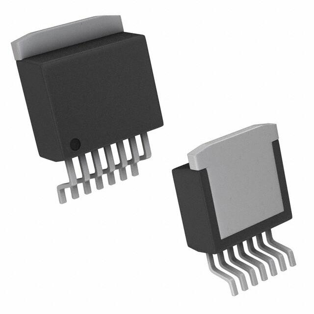
Available in 7-Pin TO-220 and TO-263 (SurfaceMount) Package
Input Voltage Range up to 60 V
150-kHz Fixed Frequency Internal Oscillator
Shutdown and Soft-Start
Out-of-Regulation Error Flag
Error Flag Delay
Low Power Standby Mode: IQ, Typically 90 μA
High Efficiency
Thermal Shutdown and Current-Limit Protection
2 Applications
•
•
•
•
Simple High-Efficiency Step-Down (Buck)
Regulators
Efficient Preregulator for Linear Regulators
On-Card Switching Regulators
Positive-to-Negative Converters
3 Description
This series of switching regulators is similar to the
LM2592HV
with
additional
supervisory
and
performance features.
Requiring a minimum number of external
components, these regulators are simple to use and
include internal frequency compensation, improved
line and load specifications, fixed-frequency oscillator,
Shutdown/Soft-start, output error flag, and flag delay.
The LM2593HV operates at a switching frequency of
150 kHz, thus allowing smaller sized filter
components than what would be needed with lower
frequency switching regulators. Available in a
standard 7-pin TO-220 package with several different
lead bend options, and a 7-pin TO-263 surface-mount
package.
Other features include a specified ±4% tolerance on
output voltage under all conditions of input voltage
and output load conditions, and ±15% on the
oscillator frequency. External shutdown is included,
featuring typically 90-μA standby current. Selfprotection features include a two stage current limit
for the output switch and an overtemperature
shutdown for complete protection under fault
conditions.
Device Information(1)
PART NUMBER
LM2593HV
The LM2593HV series of regulators are monolithic
integrated circuits that provide all the active functions
for a step-down (buck) switching regulator, capable of
driving a 2-A load with excellent line and load
regulation. These devices are available in fixed output
voltages of 3.3-V, 5-V, and an adjustable output
version.
PACKAGE
BODY SIZE (NOM)
TO-263 (7)
10.10 mm × 8.89 mm
TO-220 (7)
14.99 mm × 10.16 mm
(1) For all available packages, see the orderable addendum at
the end of the data sheet.
Typical Application (Fixed Output Voltage Versions)
Copyright © 2016, Texas Instruments Incorporated
1
An IMPORTANT NOTICE at the end of this data sheet addresses availability, warranty, changes, use in safety-critical applications,
intellectual property matters and other important disclaimers. PRODUCTION DATA.
�LM2593HV
SNVS082E – DECEMBER 2001 – REVISED MAY 2016
www.ti.com
Table of Contents
1
2
3
4
5
6
Features ..................................................................
Applications ...........................................................
Description .............................................................
Revision History.....................................................
Pin Configuration and Functions .........................
Specifications.........................................................
1
1
1
2
3
4
6.1
6.2
6.3
6.4
6.5
6.6
6.7
6.8
4
4
4
5
5
6
6
Absolute Maximum Ratings ......................................
ESD Ratings..............................................................
Recommended Operating Conditions.......................
Thermal Information ..................................................
Electrical Characteristics...........................................
Electrical Characteristics – 3.3-V Version.................
Electrical Characteristics – 5-V Version....................
Electrical Characteristics – Adjustable Voltage
Version .......................................................................
6.9 Typical Characteristics ..............................................
6
7
7
Parameter Measurement Information ................ 11
8
Detailed Description ............................................ 12
7.1 Test Circuits ............................................................ 11
8.1
8.2
8.3
8.4
9
Overview .................................................................
Functional Block Diagram .......................................
Feature Description.................................................
Device Functional Modes........................................
12
12
12
15
Application and Implementation ........................ 16
9.1 Application Information............................................ 16
9.2 Typical Application .................................................. 18
10 Power Supply Recommendations ..................... 22
11 Layout................................................................... 22
11.1 Layout Guidelines ................................................. 22
11.2 Layout Example .................................................... 22
11.3 Thermal Considerations ........................................ 23
12 Device and Documentation Support ................. 24
12.1
12.2
12.3
12.4
12.5
Documentation Support ........................................
Community Resources..........................................
Trademarks ...........................................................
Electrostatic Discharge Caution ............................
Glossary ................................................................
24
24
24
24
24
13 Mechanical, Packaging, and Orderable
Information ........................................................... 24
4 Revision History
NOTE: Page numbers for previous revisions may differ from page numbers in the current version.
Changes from Revision D (December 2011) to Revision E
•
2
Page
Added ESD Ratings table, Feature Description section, Device Functional Modes, Application and Implementation
section, Power Supply Recommendations section, Layout section, Device and Documentation Support section, and
Mechanical, Packaging, and Orderable Information section .................................................................................................. 1
Submit Documentation Feedback
Copyright © 2001–2016, Texas Instruments Incorporated
Product Folder Links: LM2593HV
�LM2593HV
www.ti.com
SNVS082E – DECEMBER 2001 – REVISED MAY 2016
5 Pin Configuration and Functions
NDZ Package
7-Pin TO-220
Top View
KTW Package
7-Pin TO-263
Top View
Not to scale
7
SD/SS
6
Feedback
5
Delay
4
Ground
3
Flag
2
Output
1
VIN
Thermal
Pad
1
2
3
4
5
6
7
VIN
Output
Flag
Ground
Delay
Feedback
SD/SS
Not to scale
Pin Functions
PIN
NO.
NAME
TYPE (1)
DESCRIPTION
1
VIN
I
This is the positive input supply for the IC switching regulator. A suitable input bypass capacitor must
be present at this pin to minimize voltage transients and to supply the switching currents needed by
the regulator.
2
Output
O
Internal switch. The voltage at this pin switches between approximately (+VIN − VSAT) and
approximately −0.5 V, with a duty cycle of VOUT/VIN.
3
Flag
O
Error flag: Open-collector output that goes active low (≤1 V) when the output of the switching
regulator is out of regulation (less than 95% of its nominal value). In this state it can sink maximum 3
mA. When not low, it can be pulled high to signal that the output of the regulator is in regulation
(power good). During power-up, it can be programmed to go high after a certain delay as set by the
Delay pin (Pin 5). The maximum rating of this pin must not be exceeded, so if the rail to which it will
be pulled up to is higher than 45 V, a resistive divider must be used instead of a single pullup resistor,
as indicated in Test Circuits.
4
Ground
—
Circuit ground.
O
This sets a programmable power-up delay from the moment that the output reaches regulation, to the
high signal output (power good) on Pin 3. A capacitor on this pin starts charging up by means on an
internal (3 μA) current source when the regulated output rises to within 5% of its nominal value. Pin 3
goes high (with an external pullup) when the voltage on the capacitor on Pin 5 exceeds 1.3 V. The
voltage on this pin is clamped internally to about 1.7 V. If the regulated output drops out of regulation
(less than 95% of its nominal value), the capacitor on Pin 5 is rapidly discharged internally and Pin 3
is forced low in about 1/1000th of the set power-up delay time. (2)
I
Senses the regulated output voltage to complete the feedback loop. This pin is directly connected to
the Output for the fixed voltage versions, but is set to 1.23 V by means of a resistive divider from the
output for the adjustable version. If a feedforward capacitor is used (adjustable version), then a
negative voltage spike is generated on this pin whenever the output is shorted. This happens
because the feedforward capacitor cannot discharge fast enough, and because one end of it is
dragged to Ground, the other end goes momentarily negative. To prevent the energy rating of this pin
from being exceeded, a small-signal Schottky diode to Ground is recommended for DC input voltages
above 40 V whenever a feedforward capacitor is present (see Test Circuits). Feedforward capacitor
values larger than 0.1 μF are not recommended for the same reason, whatever be the DC input
voltage. (2)
5
6
(1)
(2)
Delay
Feedback
G = Ground, I = Input, O = Output
If any of these pins are not used, the respective pin can be left open.
Submit Documentation Feedback
Copyright © 2001–2016, Texas Instruments Incorporated
Product Folder Links: LM2593HV
3
�LM2593HV
SNVS082E – DECEMBER 2001 – REVISED MAY 2016
www.ti.com
Pin Functions (continued)
PIN
NO.
NAME
7
TYPE (1)
DESCRIPTION
I
Shutdown/Soft-start: The regulator is in shutdown mode, drawing about 90 μA, when this pin is driven
to a low level (≤ 0.6 V), and is in normal operation when this Pin is left floating (internal pull-up) or
driven to a high level (≥ 2 V). The typical value of the threshold is 1.3 V and the pin is internally
clamped to a maximum of about 7 V. If it is driven higher than the clamp voltage, it must be ensured
by means of an external resistor that the current into the pin does not exceed 1 mA. The duty cycle is
minimum (0%) if this Pin is below 1.8 V, and increases as the voltage on the pin is increased. The
maximum duty cycle (100%) occurs when this pin is at 2.8 V or higher. So adding a capacitor to this
pin produces a soft-start feature. An internal current source charges the capacitor from zero to its
internally clamped value. The charging current is about 5 μA when the pin is below 1.3 V but is
reduced to only 1.6 μA above 1.3 V, so as to allow the use of smaller soft-start capacitors. (2)
SD/SS
6 Specifications
6.1 Absolute Maximum Ratings
over operating free-air temperature range (unless otherwise noted) (1)
MAX
UNIT
Maximum supply voltage, VIN
MIN
63
V
SD/SS pin input voltage (2)
6
V
1.5
V
Delay pin voltage (2)
Flag pin voltage
–0.3
45
V
Feedback pin voltage
–0.3
25
V
–1
V
Output voltage to ground, steady-state
Power dissipation
Lead temperature
Internally limited
S package
Vapor phase (60 s)
215
Infrared (10 s)
245
T package, soldering (10 s)
260
Maximum junction temperature
Storage temperature, Tstg
(1)
(2)
°C
–65
150
°C
150
°C
Stresses beyond those listed under Absolute Maximum Ratings may cause permanent damage to the device. These are stress ratings
only, which do not imply functional operation of the device at these or any other conditions beyond those indicated under Recommended
Operating Conditions. Exposure to absolute-maximum-rated conditions for extended periods may affect device reliability.
Voltage internally clamped. If clamp voltage is exceeded, limit current to a maximum of 1 mA.
6.2 ESD Ratings
V(ESD)
(1)
(2)
Electrostatic discharge
Human-body model (HBM), per ANSI/ESDA/JEDEC JS-001 (1) (2)
VALUE
UNIT
±2000
V
JEDEC document JEP155 states that 500-V HBM allows safe manufacturing with a standard ESD control process.
The human body model is a 100-pF capacitor discharged through a 1.5-k resistor into each pin.
6.3 Recommended Operating Conditions
over operating free-air temperature range (unless otherwise noted)
MIN
TJ
4
MAX
UNIT
Supply voltage
4.5
60
V
Temperature
–40
125
°C
Submit Documentation Feedback
Copyright © 2001–2016, Texas Instruments Incorporated
Product Folder Links: LM2593HV
�LM2593HV
www.ti.com
SNVS082E – DECEMBER 2001 – REVISED MAY 2016
6.4 Thermal Information
LM2593HV
THERMAL METRIC (1)
NDZ (TO-220)
KTW (TO-263)
7 PINS
7 PINS
UNIT
50 (3)
RθJA
Junction-to-ambient thermal resistance
50
(2)
30 (4)
°C/W
20 (5)
RθJC(top)
Junction-to-case (top) thermal resistance
2
2
°C/W
RθJB
Junction-to-board thermal resistance
—
—
°C/W
ψJT
Junction-to-top characterization parameter
—
—
°C/W
ψJB
Junction-to-board characterization parameter
—
—
°C/W
RθJC(bot)
Junction-to-case (bottom) thermal resistance
—
—
°C/W
(1)
(2)
(3)
(4)
(5)
For more information about traditional and new thermal metrics, see the Semiconductor and IC Package Thermal Metrics application
report, SPRA953.
Junction to ambient thermal resistance (no external heat sink) for the package mounted TO-220 package mounted vertically, with the
leads soldered to a printed-circuit board with (1 oz) copper area of approximately 1 in2.
Junction to ambient thermal resistance with the TO-263 package tab soldered to a single-sided printed-circuit board with 0.5 in2 of (1 oz)
copper area.
Junction to ambient thermal resistance with the TO-263 package tab soldered to a single-sided printed-circuit board with 2.5 in2 of (1 oz)
copper area.
Junction to ambient thermal resistance with the TO-263 package tab soldered to a double-sided printed-circuit board with 3 in2 of (1 oz)
copper area on the LM2593HVS side of the board, and approximately 16 in2 of copper on the other side of the printed-circuit board.
6.5 Electrical Characteristics
TJ = 25°C, VIN = 12 V for the 3.3-V, 5-V, and adjustable versions, and ILOAD = 500 mA (unless otherwise noted)
MIN (1)
TYP (2)
MAX (1)
50
10
100
TJ = 25°C
127
150
173
TJ = –40°C to 125°C
110
PARAMETER
Ib
fO
Feedback bias current
Oscillator frequency (3)
TEST CONDITIONS
Adjustable version only, VFB = 1.3 V
Saturation voltage
IOUT = 2 A; no diode, inductor
or capacitor connected to
output pin (4); Feedback pin
removed from output and
connected to 0 V to force the
output transistor switch ON (5)
Max duty cycle (ON)
Feedback pin removed from output and connected to 0
V to force the output transistor switch ON
Min duty cycle (OFF)
Feedback pin removed from output and connected to
12 V for the 3.3-V, 5-V, and the adjustable versions to
force the output transistor switch OFF
Switch current limit
Peak current; no diode,
TJ = 25°C
inductor or capacitor connected
to output pin; Feedback pin
removed from output and
TJ = –40°C to 125°C
connected to 0 V to force the
output transistor switch ON
IL
Output leakage current
Feedback pin removed from output and connected to
12 V for the 3.3-V, 5-V, and the adjustable version to
force the output transistor switch OFF; VIN = 60 V,
output = 0 V,
output = −1 V
IQ
Operating quiescent current
SD and SS pin open, Feedback pin removed from
output and connected to 12 V for the 3.3-V, 5-V, and
the adjustable version to force the output transistor
switch OFF
VSAT
DC
ICLIM
(1)
(2)
(3)
(4)
(5)
TJ = 25°C
173
1.1
TJ = –40°C to 125°C
UNIT
nA
kHz
1.3
1.4
V
100%
0%
2.4
3
2.3
50
3.7
4
A
5
30
mA
5
10
mA
All limits specified at room temperature unless otherwise noted. All room temperature limits are 100% production tested. All limits at
temperature extremes are ensured via correlation using standard Statistical Quality Control (SQC) methods. All limits are used to
calculate Average Outgoing Quality Level (AOQL).
Typical numbers are at 25°C and represent the most likely norm.
The switching frequency is reduced when the second stage current limit is activated. The amount of reduction is determined by the
severity of current overload.
No diode, inductor or capacitor connected to output pin.
Feedback pin removed from output and connected to 0 V to force the output transistor switch ON.
Submit Documentation Feedback
Copyright © 2001–2016, Texas Instruments Incorporated
Product Folder Links: LM2593HV
5
�LM2593HV
SNVS082E – DECEMBER 2001 – REVISED MAY 2016
www.ti.com
Electrical Characteristics (continued)
TJ = 25°C, VIN = 12 V for the 3.3-V, 5-V, and adjustable versions, and ILOAD = 500 mA (unless otherwise noted)
PARAMETER
ISTBY
MIN (1)
TEST CONDITIONS
SD and SS pin = 0 V,
VIN = 60 V
Standby quiescent current
TJ = 25°C
TYP (2)
MAX (1)
90
200
TJ = –40°C to 125°C
250
UNIT
µA
SHUTDOWN AND SOFT-START CONTROL
VSD
Shutdown threshold voltage
VSS
Soft-start voltage
ISD
ISS
Low (shutdown mode)
1.3
High (soft-start mode)
0.6
2
V
VOUT = 20% of nominal output voltage
2
VOUT = 100% of nominal output voltage
3
Shutdown current
VSHUTDOWN = 0.5 V
5
10
µA
Soft-start current
VSoft-start = 2.5 V
1.5
5
µA
Regulator dropout detector
Low (flag ON)
V
96%
Threshold voltage
Low (flag ON)
VFSAT
Flag output saturation voltage
ISINK = 3 mA, VDELAY = 0.5 V
92%
IFL
Flag output leakage current
VFLAG = 60 V
Delay pin threshold voltage
Low (flag ON), high (flag OFF) and VOUT regulated
Delay pin source current
VDELAY = 0.5 V
Delay pin saturation
Low (flag ON)
98%
0.3
µA
0.7
0.3
1
1.21
1.25
1.29
V
V
3
6
µA
350
70
400
mV
MIN
TYP
MAX
UNIT
TJ = 25°C
3.168
3.3
3.432
TJ = –40°C to 125°C
3.135
6.6 Electrical Characteristics – 3.3-V Version
TJ = 25°C (unless otherwise noted)
PARAMETER
TEST CONDITIONS
SYSTEM PARAMETERS
VOUT
Output voltage
4.75 V ≤ VIN ≤ 60 V,
0.2 A ≤ ILOAD ≤ 2 A
η
Efficiency
VIN = 12 V, ILOAD = 2 A
3.465
V
76%
6.7 Electrical Characteristics – 5-V Version
TJ = 25°C (unless otherwise noted)
PARAMETER
TEST CONDITIONS
TJ = 25°C
V
Output voltage
7 V ≤ VIN ≤ 60 V,
0.2 A ≤ILOAD ≤ 2 A
η
Efficiency
VIN = 12 V, ILOAD = 2 A
TJ = –40°C to 125°C
MIN
TYP
MAX
4.8
5
5.2
4.75
5.25
UNIT
V
81%
6.8 Electrical Characteristics – Adjustable Voltage Version
TJ = 25°C (unless otherwise noted)
PARAMETER
TEST CONDITIONS
VFB
Feedback voltage
4.5 V ≤ VIN ≤ 60 V,
0.2 A ≤ ILOAD ≤ 2 A,
VOUT programmed for 3 V
(see Test Circuits)
η
Efficiency
VIN = 12 V, VOUT = 3 V, ILOAD = 2 A
6
TJ = 25°C
TJ = –40°C to 125°C
Submit Documentation Feedback
MIN
TYP
MAX
1.193
1.23
1.267
1.18
1.28
UNIT
V
75%
Copyright © 2001–2016, Texas Instruments Incorporated
Product Folder Links: LM2593HV
�LM2593HV
www.ti.com
SNVS082E – DECEMBER 2001 – REVISED MAY 2016
6.9 Typical Characteristics
Figure 1. Normalized Output Voltage
Figure 2. Line Regulation
Figure 3. Efficiency
Figure 4. Switch Saturation Voltage
Figure 5. Switch Current Limit
Figure 6. Dropout Voltage
Submit Documentation Feedback
Copyright © 2001–2016, Texas Instruments Incorporated
Product Folder Links: LM2593HV
7
�LM2593HV
SNVS082E – DECEMBER 2001 – REVISED MAY 2016
www.ti.com
Typical Characteristics (continued)
8
Figure 7. Operating Quiescent Current
Figure 8. Shutdown Quiescent Current
Figure 9. Minimum Operating Supply Voltage
Figure 10. Feedback Pin Bias Current
Figure 11. Flag Saturation Voltage
Figure 12. Switching Frequency
Submit Documentation Feedback
Copyright © 2001–2016, Texas Instruments Incorporated
Product Folder Links: LM2593HV
�LM2593HV
www.ti.com
SNVS082E – DECEMBER 2001 – REVISED MAY 2016
Typical Characteristics (continued)
Figure 13. Soft-Start
Figure 14. Shutdown/Soft-Start Current
Figure 15. Delay Pin Current
Figure 16. Soft-Start Response
Figure 17. Shutdown/Soft-Start Threshold Voltage
Figure 18. Internal Gain-Phase Characteristics
Submit Documentation Feedback
Copyright © 2001–2016, Texas Instruments Incorporated
Product Folder Links: LM2593HV
9
�LM2593HV
SNVS082E – DECEMBER 2001 – REVISED MAY 2016
www.ti.com
Typical Characteristics (continued)
Horizontal Time Base: 2 µs/div.
VIN = 20 V, VOUT = 5 V, ILOAD = 2 A,
L = 32 µH, COUT = 220 µF, COUT ESR = 50 mΩ
Output Pin Voltage, 10 V/div.
Inductor Current, 1 A/div.
Output Ripple Voltage, 50 mV/div.
Figure 19. Continuous Mode Switching Waveforms
Horizontal Time Base: 2 µs/div.
VIN = 20 V, VOUT = 5 V, ILOAD = 500 mA,
L = 10 µH, COUT = 330 µF, COUT ESR = 50 mΩ
Output Pin Voltage, 10 V/div.
Inductor Current, 0.5 A/div.
Output Ripple Voltage, 100 mV/div.
Figure 20. Discontinuous Mode Switching Waveforms
Horizontal Time Base: 50 µs/div.
VIN = 20 V, VOUT = 5 V, ILOAD = 500 mA to 2 A,
L = 32 µH, COUT = 220 µF, COUT ESR = 50 mΩ
Output Voltage, 100 mV/div. (AC)
500-mA to 2-A Load Pulse
Figure 21. Load Transient Response
for Continuous Mode
Horizontal Time Base: 200 µs/div.
VIN = 20 V, VOUT = 5 V, ILOAD = 500 mA to 2 A,
L = 10 µH, COUT = 330 µF, COUT ESR = 50 mΩ
Output Voltage, 100 mV/div. (AC)
500-mA to 2-A Load Pulse
Figure 22. Load Transient Response
for Discontinuous Mode
10
Submit Documentation Feedback
Copyright © 2001–2016, Texas Instruments Incorporated
Product Folder Links: LM2593HV
�LM2593HV
www.ti.com
SNVS082E – DECEMBER 2001 – REVISED MAY 2016
7 Parameter Measurement Information
7.1 Test Circuits
Component Values shown are for VIN = 15 V,
VOUT = 5 V, ILOAD = 2 A.
CIN — 470-µF, 50-V aluminum electrolytic Nichicon PM Series
COUT — 220-µF, 25-V aluminum electrolytic Nichcon PM Series
D1 — 3.3-A, 60-V Schottky Rectifier, 21DQ06 (international rectifier)
L1 — 33 µH, see Inductors Selection Procedure
Figure 23. Fixed Output Voltage Versions
Select R1 to be approximately 1 kΩ, use a 1% resistor for best stability.
Component values shown are for VIN = 20 V,
VOUT = 10 V, ILOAD = 2 A.
CIN — 470-µF, 35-V aluminum electrolytic Nichicon PM Series
COUT — 220-µF, 35-V aluminum electrolytic Nichicon PM Series
D1 — 3.3-A, 60-V Schottky Rectifier, 21DQ06 (international rectifier)
L1 — 47 µH, see Inductors Selection Procedure
R1 — 1 kΩ, 1%
R2 — 7.15 k, 1%
CFF — 3.3 nF
Typical Values
CSS — 0.1 µF
CDELAY — 0.1 µF
RPULL UP — 4.7 k (use 22 k if VOUT is ≥ 45 V)
† Resistive divider is required to avoid exceeding maximum rating of 45 V, 3 mA on or into flag pin.
†† Small signal Schottky diode to prevent damage to feedback pin by negative spike when output is shorted (CFF not
being able to discharge immediately will drag feedback pin below ground). Required if VIN > 40 V.
Figure 24. Adjustable Output Voltage Versions
Submit Documentation Feedback
Copyright © 2001–2016, Texas Instruments Incorporated
Product Folder Links: LM2593HV
11
�LM2593HV
SNVS082E – DECEMBER 2001 – REVISED MAY 2016
www.ti.com
8 Detailed Description
8.1 Overview
The LM2593HV SIMPLE SWITCHER® regulator is an easy-to-use, non-synchronous, step-down DC-DC
converter with a wide input voltage range up to 60 V. It is capable of delivering up to 2-A DC load current with
excellent line and load regulation. These devices are available in fixed output voltages of 3.3-V, 5-V, and an
adjustable output version. The family requires few external components and the pin arrangement was designed
for simple, optimum PCB layout.
8.2 Functional Block Diagram
Copyright © 2016, Texas Instruments Incorporated
8.3 Feature Description
8.3.1 Undervoltage Lockout
Some applications require the regulator to remain off until the input voltage reaches a predetermined voltage.
Figure 25 contains a undervoltage lockout circuit for a buck configuration, while Figure 26 and Figure 27 are for
the inverting types (only the circuitry pertaining to the undervoltage lockout is shown). Figure 25 uses a Zener
diode to establish the threshold voltage when the switcher begins operating. When the input voltage is less than
the Zener voltage, resistors R1 and R2 hold the Shutdown/Soft-Start pin low, keeping the regulator in the
shutdown mode. As the input voltage exceeds the Zener voltage, the Zener conducts, pulling the Shutdown/SoftStart pin high, allowing the regulator to begin switching. The threshold voltage for the undervoltage lockout
feature is approximately 1.5 V greater than the Zener voltage.
12
Submit Documentation Feedback
Copyright © 2001–2016, Texas Instruments Incorporated
Product Folder Links: LM2593HV
�LM2593HV
www.ti.com
SNVS082E – DECEMBER 2001 – REVISED MAY 2016
Feature Description (continued)
Copyright © 2016, Texas Instruments Incorporated
Figure 25. Undervoltage Lockout for a Buck Regulator
Figure 26 and Figure 27 apply the same feature to an inverting circuit. Figure 26 features a constant threshold
voltage for turnon and turnoff (Zener voltage plus approximately 1 V). If hysteresis is needed, the circuit in
Figure 27 has a turnon voltage which is different than the turnoff voltage. The amount of hysteresis is
approximately equal to the value of the output voltage. Because the SD/SS pin has an internal 7-V Zener clamp,
R2 is needed to limit the current into this pin to approximately 1 mA when Q1 is on.
Copyright © 2016, Texas Instruments Incorporated
Figure 26. Undervoltage Lockout Without Hysteresis for an Inverting Regulator
Copyright © 2016, Texas Instruments Incorporated
Figure 27. Undervoltage Lockout With Hysteresis for an Inverting Regulator
Submit Documentation Feedback
Copyright © 2001–2016, Texas Instruments Incorporated
Product Folder Links: LM2593HV
13
�LM2593HV
SNVS082E – DECEMBER 2001 – REVISED MAY 2016
www.ti.com
Feature Description (continued)
8.3.2 Negative Voltage Charge Pump
Occasionally a low current negative voltage is needed for biasing parts of a circuit. A simple method of
generating a negative voltage using a charge pump technique is shown in Figure 28. This unregulated negative
voltage is approximately equal to the positive input voltage (minus a few volts), and can supply up to a 600 mA of
output current. There is a requirement however, that there be a minimum load of 1.2 A on the regulated positive
output for the charge pump to work correctly. Also, resistor R1 is required to limit the charging current of C1 to
some value less than the LM2593HV current limit. This method of generating a negative output voltage without
an additional inductor can be used with other members of the SIMPLE SWITCHER® family, using either the buck
or boost topology.
Copyright © 2016, Texas Instruments Incorporated
Figure 28. Charge Pump for Generating a Low-Current, Negative Output Voltage
8.3.3 Shutdown/Soft-Start
This reduction in start-up current is useful in situations where the input power source is limited in the amount of
current it can deliver. In some applications, soft-start can be used to replace undervoltage lockout or delayed
start-up functions. If a very slow output voltage ramp is desired, the soft-start capacitor can be made much
larger. Many seconds or even minutes are possible. If only the shutdown feature is needed, the soft-start
capacitor can be eliminated.
Figure 29. Typical Circuit Using Shutdown/Soft-Start and Error Flag Features
14
Submit Documentation Feedback
Copyright © 2001–2016, Texas Instruments Incorporated
Product Folder Links: LM2593HV
�LM2593HV
www.ti.com
SNVS082E – DECEMBER 2001 – REVISED MAY 2016
Feature Description (continued)
10133331
Figure 30. Soft-Start, Delay, Error Output
8.4 Device Functional Modes
8.4.1 Shutdown Mode
The Shutdown/Soft-start pin provides electrical ON and OFF control for the LM2593HV. When the voltage of this
pin is less than 0.6 V, the device is in shutdown mode. The typical standby current in this mode is 90 μA.
8.4.2 Active Mode
When the Shutdown/Soft-start pin is left floating or pull above 2 V, the device starts switching and the output
voltage rises until it reaches a normal regulation voltage.
Submit Documentation Feedback
Copyright © 2001–2016, Texas Instruments Incorporated
Product Folder Links: LM2593HV
15
�LM2593HV
SNVS082E – DECEMBER 2001 – REVISED MAY 2016
www.ti.com
9 Application and Implementation
NOTE
Information in the following applications sections is not part of the TI component
specification, and TI does not warrant its accuracy or completeness. TI’s customers are
responsible for determining suitability of components for their purposes. Customers should
validate and test their design implementation to confirm system functionality.
9.1 Application Information
9.1.1 Feedforward Capacitor, CFF
(Adjustable output voltage version only)
A feedforward capacitor shown across R2 in Test Circuits is used when the output voltage is greater than 10 V or
when COUT has a very low ESR. This capacitor adds lead compensation to the feedback loop and increases the
phase margin for better loop stability. If the output voltage ripple is large (>5% of the nominal output voltage), this
ripple can be coupled to the feedback pin through the feedforward capacitor and cause the error comparator to
trigger the error flag. In this situation, adding a resistor, RFF, in series with the feedforward capacitor,
approximately 3 times R1, attenuates the ripple voltage at the feedback pin.
9.1.2 Input Capacitor, CIN
A low-ESR aluminum or tantalum bypass capacitor is needed between the input pin and ground pin. It must be
placed near the regulator using short leads. This capacitor prevents large voltage transients from appearing at
the input, and provides the instantaneous current needed each time the switch turns on. The important
parameters for the Input capacitor are the voltage rating and the RMS current rating. Because of the relatively
high RMS currents flowing in a buck regulator’s input capacitor, this capacitor must be chosen for its RMS
current rating rather than its capacitance or voltage ratings, although the capacitance value and voltage rating
are directly related to the RMS current rating. The voltage rating of the capacitor and its RMS ripple current
capability must never be exceeded.
9.1.3 Output Capacitor, COUT
An output capacitor is required to filter the output and provide regulator loop stability. Low impedance or low ESR
Electrolytic or solid tantalum capacitors designed for switching regulator applications must be used. When
selecting an output capacitor, the important capacitor parameters are; the 100-kHz Equivalent Series Resistance
(ESR), the RMS ripple current rating, voltage rating, and capacitance value. For the output capacitor, the ESR
value is the most important parameter. The ESR must generally not be less than 100 mW or there will be loop
instability. If the ESR is too large, efficiency and output voltage ripple are effected. So ESR must be chosen
carefully.
9.1.4 Catch Diode
Buck regulators require a diode to provide a return path for the inductor current when the switch turns off. This
must be a fast diode and must be placed close to the LM2593HV using short leads and short printed-circuit
traces.
Because of their very fast switching speed and low forward voltage drop, Schottky diodes provide the best
performance, especially in low output voltage applications (5 V and lower). Ultra-fast recovery, or high-efficiency
rectifiers are also a good choice, but some types with an abrupt turnoff characteristic may cause instability or
EMI problems. Ultra-fast recovery diodes typically have reverse recovery times of 50 ns or less. The diode must
be chosen for its average or RMS current rating and maximum voltage rating. The voltage rating of the diode
must be greater than the DC input voltage (not the output voltage).
16
Submit Documentation Feedback
Copyright © 2001–2016, Texas Instruments Incorporated
Product Folder Links: LM2593HV
�LM2593HV
www.ti.com
SNVS082E – DECEMBER 2001 – REVISED MAY 2016
Application Information (continued)
9.1.5 lnverting Regulator
The circuit in Figure 31 converts a positive input voltage to a negative output voltage with a common ground. The
circuit operates by bootstrapping the regulator’s ground pin to the negative output voltage, then grounding the
feedback pin, the regulator senses the inverted output voltage and regulates it. This example uses the
LM2593HV 5-V to generate a −5-V output, but other output voltages are possible by selecting other output
voltage versions, including the adjustable version. Because this regulator topology can produce an output voltage
that is either greater than or less than the input voltage, the maximum output current greatly depends on both the
input and output voltage. To determine how much load current is possible before the internal device current limit
is reached (and power limiting occurs), the system must be evaluated as a buck-boost configuration rather than
as a buck. The peak switch current in amperes, for such a configuration is given as Equation 1.
æ V + VOUT ö
VIN ´ VOUT ´ 106
I PEAK = I LOAD ´ ç IN
÷+
VIN
è
ø 2 ´ L ´ f ´ (VIN + VOUT )
where
•
•
L is in μH
f is in Hz
(1)
The maximum possible load current ILOAD is limited by the requirement that IPEAK ≤ ICLIM. While checking for this,
take ICLIM to be the lowest possible current limit value (minimum across tolerance and temperature is 2.3 A for
the LM2593HV). Also to account for inductor tolerances, take the minimum value of Inductance for L in
Equation 1 (typically 20% less than the nominal value). Further, the above equation disregards the drop across
the switch and the diode. This is equivalent to assuming 100% efficiency, which is never so. Therefore expect
IPEAK to be an additional 10-20% higher than calculated from Equation 1. See also Application Note AN-1197
Selecting Inductors for Buck Converters (SNVA038) for examples based on positive to negative configuration.
The maximum voltage appearing across the regulator is the absolute sum of the input and output voltage. This
must be limited to a maximum of 60 V. In this example, when converting 20 V to −5 V, the regulator would see
25 V between the input pin and ground pin. The LM2593HV has a maximum input voltage rating of 60 V. An
additional diode is required in this regulator configuration. Diode D1 is used to isolate input voltage ripple or
noise from coupling through the CIN capacitor to the output, under light or no load conditions. Also, this diode
isolation changes the topology to closely resemble a buck configuration thus providing good closed-loop stability.
A Schottky diode is recommended for low input voltages, (because of its lower voltage drop) but for higher input
voltages, a IN5400 diode could be used. Because of differences in the operation of the inverting regulator, the
standard design procedure is not used to select the inductor value. In the majority of designs, a 33-μH, 4-A
inductor is the best choice. Capacitor selection can also be narrowed down to just a few values. This type of
inverting regulator can require relatively large amounts of input current when starting up, even with light loads.
Input currents as high as the LM2593HV current limit (approximately 4 A) are needed for 2 ms or more, until the
output reaches its nominal output voltage. The actual time depends on the output voltage and the size of the
output capacitor. Input power sources that are current limited or sources that can not deliver these currents
without getting loaded down, may not work correctly. Because of the relatively high start-up currents required by
the inverting topology, the soft-start feature shown in Figure 31 is recommended. Also shown in Figure 31 are
several shutdown methods for the inverting configuration. With the inverting configuration, some level shifting is
required, because the ground pin of the regulator is no longer at ground, but is now at the negative output
voltage. The shutdown methods shown accept ground referenced shutdown signals.
Submit Documentation Feedback
Copyright © 2001–2016, Texas Instruments Incorporated
Product Folder Links: LM2593HV
17
�LM2593HV
SNVS082E – DECEMBER 2001 – REVISED MAY 2016
www.ti.com
Application Information (continued)
Figure 31. Inverting −5 V Regulator With Shutdown and Soft-Start
9.2 Typical Application
Copyright © 2016, Texas Instruments Incorporated
Figure 32. LM2593HV 5-V Application Schematic
9.2.1 Design Requirements
Table 1 lists the example values for this typical application.
Table 1. Application Example Parameters
DESIGN PARAMETER
18
EXAMPLE VALUE
Regulated output voltage (3.3 V, 5 V, or adjustable), VOUT
5V
Maximum input voltage, VIN(max)
24 V
Maximum load current, ILOAD(max)
1A
Switching frequency, F
Fixed at a nominal 150 kHz
Submit Documentation Feedback
Copyright © 2001–2016, Texas Instruments Incorporated
Product Folder Links: LM2593HV
�LM2593HV
www.ti.com
SNVS082E – DECEMBER 2001 – REVISED MAY 2016
9.2.2 Detailed Design Procedure
9.2.2.1 Inductors Selection Procedure
See application note AN-1197 Selecting Inductors for Buck Converters (SNVA038) for detailed information on
inductor selection. For a quick-start, see the nomographs provided in Figure 33 to Figure 35. To widen the
choices to a more general selection of available inductors, the nomographs provide the required inductance and
also the energy in the core expressed in microjoules (μJ), as an alternative to just prescribing custom parts. The
following points must be highlighted:
1. The energy values shown on the nomographs apply to steady operation at the corresponding x-coordinate
(rated maximum load current). However under start-up, without soft-start, or a short-circuit on the output, the
current in the inductor momentarily and repetitively hits the current limit ICLIM of the device, and this current
could be much higher than the rated load, ILOAD. This represents an overload situation, and can cause the
inductor to saturate (if it has been designed only to handle the energy of steady operation). However most
types of core structures used for such applications have a large inherent air gap (for example powdered iron
types or ferrite rod inductors), and so the inductance does not fall off too sharply under an overload. The
device is usually able to protect itself by not allowing the current to ever exceed ICLIM. But if the DC input
voltage to the regulator is over 40 V, the current can slew up so fast under core saturation, that the device
may not be able to act fast enough to restrict the current. The current can then rise without limit till
destruction of the device takes place. Therefore to ensure reliability, TI recommends, that if the DC input
voltage exceeds 40 V, the inductor must always be sized to handle an instantaneous current equal to ICLIM
without saturating, irrespective of the type of core structure or material.
2. Use Equation 2 to calculate the energy under steady operation.
1
e = ´ L ´ IPEAK 2 mJ
2
where
•
•
L is in μH
IPEAK is the peak of the inductor current waveform with the regulator delivering ILOAD
(2)
These are the energy values shown in the nomographs. See Example 1.
3. The energy under overload is Equation 3.
1
e = ´ L ´ ICLIM2 mJ
2
where
•
•
L is in μH
IPEAK is the peak of the inductor current waveform with the regulator delivering ILOAD
(3)
If VIN > 40 V, the inductor must be sized to handle eCLIM instead of the steady energy values. The worst case
ICLIM for the LM2593HV is 4 A. The energy rating depends on the inductance. See Example 2.
4. The nomographs were generated by allowing a greater amount of percentage current ripple in the inductor
as the maximum rated load decreases (see Figure 36). This was done to permit the use of smaller inductors
at light loads. However, Figure 36 shows only the median value of the current ripple. In reality there may be
a great spread around this because the nomographs approximate the exact calculated inductance to
standard available values. It is a good idea to refer to AN-1197 Selecting Inductors for Buck Converters
(SNVA038) for detailed calculations if a certain maximum inductor current ripple is required for various
possible reasons. Also consider the rather wide tolerance on the nominal inductance of commercial
inductors.
5. Figure 35 shows the inductor selection curves for the adjustable version. The y-axis is Et, in Vμs. It is the
applied volts across the inductor during the ON time of the switch (VIN-VSAT-VOUT) multiplied by the time for
which the switch is on in μs. See Example 3.
9.2.2.1.1 Example 1: VIN ≤ 40 V, 5-V Version, VIN = 24 V, Output = 5 V at 1 A
1. A first pass inductor selection is based upon inductance and rated maximum load current. Choose an
inductor with the inductance value indicated by the nomograph (see Figure 34) and a current rating equal to
the maximum load current. Therefore, quick-select a 68-μH, 1-A inductor (designed for 150-kHz operation)
for this application.
Submit Documentation Feedback
Copyright © 2001–2016, Texas Instruments Incorporated
Product Folder Links: LM2593HV
19
�LM2593HV
SNVS082E – DECEMBER 2001 – REVISED MAY 2016
www.ti.com
2. Confirm that it is rated to handle 50 μJ (see Figure 34) by either estimating the peak current or by a detailed
calculation as shown in AN-1197 Selecting Inductors for Buck Converters (SNVA038), and also that the
losses are acceptable.
9.2.2.1.2 Example 2: VIN > 40 V, 5-V version, VIN = 48 V, Output = 5 V at 1.5 A
1. A first pass inductor selection is based upon inductance and the switch currrent limit. Choose an inductor
with the inductance value indicated by the nomograph (see Figure 34) and a current rating equal to ICLIM.
Therefore, quick-select a 68-μH, 4-A inductor (designed for 150-kHz operation) for this application.
2. Confirm that it is rated to handle eCLIM by the procedure shown in AN-1197 Selecting Inductors for Buck
Converters (SNVA038) and that the losses are acceptable. Here eCLIM is Equation 4.
1
eCLIM = ´ 68 ´ 42 = 544 mJ
(4)
2
9.2.2.1.3 Example 3: VIN ≤ 40 V, Adjustable Version, VIN = 20 V, Output = 10 V at 2 A
1. Because input voltage is less than 40 V, a first pass inductor selection is based upon inductance and rated
maximum load current. Choose an inductor with the inductance value indicated by the nomograph Figure 35
and a current rating equal to the maximum load. But first calculate Et for the given application. The duty
cycle is Equation 5.
VOUT + VD
D=
VIN - VSAT + VD
where
•
•
VD is the drop across the catch diode (0.5 V for a Schottky)
VSAT the drop across the switch (1.5 V)
So this yields Equation 6.
10 + 0.5
= 0.55
D=
20 - 1.5 + 0.5
2. The switch ON time is calculated with Equation 7.
D
t ON = ´ 106 ms
f
(5)
(6)
where
•
f is the switching frequency in Hz
(7)
So this yields Equation 8.
Et = (VIN - VSAT - VOUT )´ t ON
= (20 - 1.5 - 10 )´
0.55
´ 106 Vm sec s
150000
= 31.3 Vm sec s
(8)
3. Therefore, looking at Figure 33, quick-select a 47-μH, 2-A inductor (designed for 150-kHz operation) for this
application.
4. Confirm that it is rated to handle 200 μJ (see Figure 35) by the procedure shown in AN-1197 Selecting
Inductors for Buck Converters (SNVA038) and that the losses are acceptable. (If the DC input voltage had
been greater than 40 V, consider eCLIM as in Example 2).
This completes the simplified inductor selection procedure. For more general applications and better
optimization, refer to AN-1197 Selecting Inductors for Buck Converters (SNVA038).
20
Submit Documentation Feedback
Copyright © 2001–2016, Texas Instruments Incorporated
Product Folder Links: LM2593HV
�LM2593HV
www.ti.com
SNVS082E – DECEMBER 2001 – REVISED MAY 2016
9.2.3 Application Curves
For continuous mode operation
Figure 33. LM2593HV 3.3-V
Figure 34. LM2593HV 5-V
Figure 35. LM2593HV Adjustable Voltage
Figure 36. Current Ripple Ratio
Submit Documentation Feedback
Copyright © 2001–2016, Texas Instruments Incorporated
Product Folder Links: LM2593HV
21
�LM2593HV
SNVS082E – DECEMBER 2001 – REVISED MAY 2016
www.ti.com
10 Power Supply Recommendations
The LM2593HV is designed to operate from an input voltage supply up to 60 V. This input supply must be well
regulated and able to withstand maximum input current and maintain a stable voltage.
11 Layout
11.1 Layout Guidelines
As in any switching regulator, layout is very important. Rapid switching currents associated with wiring
inductance can generate voltage transients which can cause problems. For minimal inductance and ground
loops, with reference to Functional Block Diagram, the wires indicated by heavy lines must be wide printed-circuit
traces and must be kept as short as possible. For best results, external components must be placed as close to
the switcher lC as possible using ground plane construction or single-point grounding.
If open core inductors are used, take special care as to the location and positioning of this type of inductor.
Allowing the inductor flux to intersect sensitive feedback, lC groundpath and COUT wiring can cause problems.
When using the adjustable version, take special care as to the location of the feedback resistors and the
associated wiring. Physically place both resistors near the IC, and route the wiring away from the inductor,
especially an open core type of inductor.
11.2 Layout Example
Figure 37. Top Side (Component Side) of PCB
22
Submit Documentation Feedback
Copyright © 2001–2016, Texas Instruments Incorporated
Product Folder Links: LM2593HV
�LM2593HV
www.ti.com
SNVS082E – DECEMBER 2001 – REVISED MAY 2016
11.3 Thermal Considerations
The LM2593HV is available in two packages, a 5-pin TO-220 (T) and a 5-pin surface-mount TO-263 (S). The
TO-220 package needs a heat sink under most conditions. The size of the heat sink depends on the input
voltage, the output voltage, the load current, and the ambient temperature. Higher ambient temperatures require
more heat sinking. The TO-263 surface-mount package tab is designed to be soldered to the copper on a
printed-circuit board. The copper and the board are the heat sink for this package and the other heat-producing
components, such as the catch diode and inductor. The PCB copper area that the package is soldered to must
be at least 0.4 in2, and ideally must have 2 or more square inches of 2-oz. (0.0028 in) copper. Additional copper
area improves the thermal characteristics, but with copper areas greater than approximately 6 in2, only small
improvements in heat dissipation are realized. If further thermal improvements are needed, double-sided,
multilayer PCB with large copper areas or airflow are recommended. The curves shown in Figure 38 show the
LM2593HVS (TO-263 package) junction temperature rise above ambient temperature with a 2-A load for various
input and output voltages. This data was taken with the circuit operating as a buck switching regulator with all
components mounted on a PCB to simulate the junction temperature under actual operating conditions. This
curve can be used for a quick check for the approximate junction temperature for various conditions, but be
aware that there are many factors that can affect the junction temperature. When load currents higher than 2 A
are used, double-sided or multilayer PCBs with large copper areas or airflow might be required, especially for
high ambient temperatures and high output voltages. For the best thermal performance, wide copper traces and
generous amounts of printed-circuit board copper must be used in the board layout. (One exception to this is the
output (switch) pin, which must not have large areas of copper.) Large areas of copper provide the best transfer
of heat (lower thermal resistance) to the surrounding air, and moving air lowers the thermal resistance even
further. Package thermal resistance and junction temperature rise numbers are all approximate, and there are
many factors that affect these numbers. Some of these factors include board size, shape, thickness, position,
location, and even board temperature. Other factors are, trace width, total printed-circuit copper area, copper
thickness, single- or double-sided, multilayer board, and the amount of solder on the board. The effectiveness of
the PCB to dissipate heat also depends on the size, quantity, and spacing of other components on the board, as
well as whether the surrounding air is still or moving. Furthermore, some of these components, such as the catch
diode will add heat to the PCB and the heat can vary as the input voltage changes. For the inductor, depending
on the physical size, type of core material, and the DC resistance, it could either act as a heat sink taking heat
away from the board, or it could add heat to the board.
Figure 38. Junction Temperature Rise, TO-263
Submit Documentation Feedback
Copyright © 2001–2016, Texas Instruments Incorporated
Product Folder Links: LM2593HV
23
�LM2593HV
SNVS082E – DECEMBER 2001 – REVISED MAY 2016
www.ti.com
12 Device and Documentation Support
12.1 Documentation Support
12.1.1 Related Documentation
For related documentation see the following:
AN-1197 Selecting Inductors for Buck Converters, SNVA038
12.2 Community Resources
The following links connect to TI community resources. Linked contents are provided "AS IS" by the respective
contributors. They do not constitute TI specifications and do not necessarily reflect TI's views; see TI's Terms of
Use.
TI E2E™ Online Community TI's Engineer-to-Engineer (E2E) Community. Created to foster collaboration
among engineers. At e2e.ti.com, you can ask questions, share knowledge, explore ideas and help
solve problems with fellow engineers.
Design Support TI's Design Support Quickly find helpful E2E forums along with design support tools and
contact information for technical support.
12.3 Trademarks
E2E is a trademark of Texas Instruments.
SIMPLE SWITCHER is a registered trademark of Texas Instruments.
All other trademarks are the property of their respective owners.
12.4 Electrostatic Discharge Caution
These devices have limited built-in ESD protection. The leads should be shorted together or the device placed in conductive foam
during storage or handling to prevent electrostatic damage to the MOS gates.
12.5 Glossary
SLYZ022 — TI Glossary.
This glossary lists and explains terms, acronyms, and definitions.
13 Mechanical, Packaging, and Orderable Information
The following pages include mechanical, packaging, and orderable information. This information is the most
current data available for the designated devices. This data is subject to change without notice and revision of
this document. For browser-based versions of this data sheet, refer to the left-hand navigation.
24
Submit Documentation Feedback
Copyright © 2001–2016, Texas Instruments Incorporated
Product Folder Links: LM2593HV
�PACKAGE OPTION ADDENDUM
www.ti.com
21-Aug-2022
PACKAGING INFORMATION
Orderable Device
Status
(1)
Package Type Package Pins Package
Drawing
Qty
Eco Plan
(2)
Lead finish/
Ball material
MSL Peak Temp
Op Temp (°C)
(3)
Device Marking
Samples
(4/5)
(6)
LM2593HVS-3.3/NOPB
ACTIVE
DDPAK/
TO-263
KTW
7
45
RoHS-Exempt
& Green
SN
Level-3-245C-168 HR
-40 to 125
LM2593HVS
-3.3 P+
Samples
LM2593HVS-5.0/NOPB
ACTIVE
DDPAK/
TO-263
KTW
7
45
RoHS-Exempt
& Green
SN
Level-3-245C-168 HR
-40 to 125
LM2593HVS
-5.0 P+
Samples
LM2593HVS-ADJ
NRND
DDPAK/
TO-263
KTW
7
45
Non-RoHS
& Green
Call TI
Level-3-235C-168 HR
-40 to 125
LM2593HVS
-ADJ P+
LM2593HVS-ADJ/NOPB
ACTIVE
DDPAK/
TO-263
KTW
7
45
RoHS-Exempt
& Green
SN
Level-3-245C-168 HR
-40 to 125
LM2593HVS
-ADJ P+
Samples
LM2593HVSX-3.3/NOPB
ACTIVE
DDPAK/
TO-263
KTW
7
500
RoHS-Exempt
& Green
SN
Level-3-245C-168 HR
-40 to 125
LM2593HVS
-3.3 P+
Samples
LM2593HVSX-5.0/NOPB
ACTIVE
DDPAK/
TO-263
KTW
7
500
RoHS-Exempt
& Green
SN
Level-3-245C-168 HR
-40 to 125
LM2593HVS
-5.0 P+
Samples
LM2593HVSX-ADJ/NOPB
ACTIVE
DDPAK/
TO-263
KTW
7
500
RoHS-Exempt
& Green
SN
Level-3-245C-168 HR
-40 to 125
LM2593HVS
-ADJ P+
Samples
LM2593HVT-5.0/NOPB
ACTIVE
TO-220
NDZ
7
45
RoHS & Green
SN
Level-1-NA-UNLIM
-40 to 125
LM2593HVT
-5.0 P+
Samples
LM2593HVT-ADJ/NOPB
ACTIVE
TO-220
NDZ
7
45
RoHS & Green
SN
Level-1-NA-UNLIM
-40 to 125
LM2593HVT
-ADJ P+
Samples
(1)
The marketing status values are defined as follows:
ACTIVE: Product device recommended for new designs.
LIFEBUY: TI has announced that the device will be discontinued, and a lifetime-buy period is in effect.
NRND: Not recommended for new designs. Device is in production to support existing customers, but TI does not recommend using this part in a new design.
PREVIEW: Device has been announced but is not in production. Samples may or may not be available.
OBSOLETE: TI has discontinued the production of the device.
(2)
RoHS: TI defines "RoHS" to mean semiconductor products that are compliant with the current EU RoHS requirements for all 10 RoHS substances, including the requirement that RoHS substance
do not exceed 0.1% by weight in homogeneous materials. Where designed to be soldered at high temperatures, "RoHS" products are suitable for use in specified lead-free processes. TI may
reference these types of products as "Pb-Free".
RoHS Exempt: TI defines "RoHS Exempt" to mean products that contain lead but are compliant with EU RoHS pursuant to a specific EU RoHS exemption.
Green: TI defines "Green" to mean the content of Chlorine (Cl) and Bromine (Br) based flame retardants meet JS709B low halogen requirements of


 工商网监
湘ICP备2023018690号
工商网监
湘ICP备2023018690号
