LM2596
ZHCSKU0F – NOVEMBER 1999 – REVISED APRIL 2021
LM2596 SIMPLE SWITCHER® 电源转换器 150kHz
3A 降压稳压器
1 特性
3 说明
• 推出的新产品:LMR33630 36V、3A、400kHz 同
步转换器
• 3.3V、5V、12V 和可调输出版本
• 可调输出电压范围:1.2V 至 37V,在各种线路和负
载条件下的最高电压容差为 ±4%
• 采用 TO-220 和 TO-263 封装
• 输出负载电流为 3A
• 输入电压范围高达 40V
• 只需要四个外部元件
• 出色的线路和负载调节规格
• 150kHz 固定频率内部振荡器
• TTL 关断功能
• 低功耗待机模式,IQ 典型值为 80μA
• 高效率
• 使用现成的标准电感器
• 热关断和电流限制保护
• 可使用 LM2596 并借助 WEBENCH Power
Designer 创建定制设计方案
LM2596 系列稳压器是为降压开关稳压器提供所有有效
功能的单片集成电路,能够驱动 3A 的负载,并且拥有
出色的线路和负载调节性能。这些器件可提供 3.3V、
5V、12V 固定输出电压和可调节输出电压版本。
2 应用
•
•
•
•
这类稳压器不仅需要很少的外部元件,而且简单易用,
还具有内部频率补偿和固定频率振荡器。
LM2596 系列在 150kHz 的开关频率下运行,因此采用
的滤波器组件比更低频率的开关稳压器所需的组件尺寸
更小。可采用具有多种不同引线折弯选项的标准 5 引
脚 TO-220 封装,以及 5 引脚 TO-263 表面贴装封装。
新产品 LMR33630 提供更低的 BOM 成本、更高的效
率、更小的解决方案尺寸(减小 85%)以及诸多其他
特性。开始使用 LMR33630 进行 WEBENCH 设计。
器件型号
LM2596
(1)
电器
电网基础设施
EPOS
家庭影院
封装(1)
封装尺寸(标称值)
TO-220 (5)
14.986mm × 10.16mm
TO-263 (5)
10.10mm × 8.89mm
如需了解所有可用封装,请参阅数据表末尾的可订购产品附
录。
(固定输出电压版本)
典型应用
本文档旨在为方便起见,提供有关 TI 产品中文版本的信息,以确认产品的概要。有关适用的官方英文版本的最新信息,请访问
www.ti.com,其内容始终优先。TI 不保证翻译的准确性和有效性。在实际设计之前,请务必参考最新版本的英文版本。
English Data Sheet: SNVS124
�LM2596
www.ti.com.cn
ZHCSKU0F – NOVEMBER 1999 – REVISED APRIL 2021
Table of Contents
1 特性................................................................................... 1
2 应用................................................................................... 1
3 说明................................................................................... 1
4 Revision History.............................................................. 2
5 Description (continued).................................................. 3
6 Pin Configuration and Functions...................................4
7 Specifications.................................................................. 5
7.1 Absolute Maximum Ratings........................................ 5
7.2 ESD Ratings............................................................... 5
7.3 Operating Conditions.................................................. 5
7.4 Thermal Information....................................................5
7.5 Electrical Characteristics – 3.3-V Version................. 6
7.6 Electrical Characteristics – 5-V Version.................... 6
7.7 Electrical Characteristics – 12-V Version.................. 6
7.8 Electrical Characteristics – Adjustable Voltage
Version.......................................................................... 6
7.9 Electrical Characteristics – All Output Voltage
Versions.........................................................................7
7.10 Typical Characteristics.............................................. 8
8 Detailed Description...................................................... 11
8.1 Overview................................................................... 11
8.2 Functional Block Diagram......................................... 11
8.3 Feature Description...................................................11
8.4 Device Functional Modes..........................................15
9 Application and Implementation.................................. 16
9.1 Application Information............................................. 16
9.2 Typical Applications.................................................. 23
10 Power Supply Recommendations..............................32
11 Layout........................................................................... 33
11.1 Layout Guidelines................................................... 33
11.2 Layout Examples.....................................................33
11.3 Thermal Considerations.......................................... 35
12 Device and Documentation Support..........................37
12.1 Device Support....................................................... 37
12.2 接收文档更新通知................................................... 37
12.3 支持资源..................................................................37
12.4 Trademarks............................................................. 37
12.5 静电放电警告.......................................................... 37
12.6 术语表..................................................................... 37
13 Mechanical, Packaging, and Orderable
Information.................................................................... 37
4 Revision History
注:以前版本的页码可能与当前版本的页码不同
Changes from Revision E (February 2020) to Revision F (April 2021)
Page
• 删除了对器件比较表的引用.................................................................................................................................1
• 更新了整个文档中的表格、图和交叉参考的编号格式......................................................................................... 1
Changes from Revision D (May 2016) to Revision E (February 2020)
Page
• 在节 1 中添加了指向 LMR33630 产品文件夹的链接...........................................................................................1
• 更新了节 3 以添加 LMR33630 产品页、器件比较表和 WEBENCH 链接........................................................... 1
• 将封装从 7 引脚更改为 5 引脚............................................................................................................................ 1
Changes from Revision C (April 2013) to Revision D (February 2016)
Page
• 添加了 ESD 等级 表、特性说明 部分、器件功能模式、应用和实施 部分、电源相关建议 部分、布局 部分、器
件和文档支持 部分以及机械、封装和可订购信息 部分....................................................................................... 1
• 删除了对设计软件 Switchers Made Simple 的所有引用..................................................................................... 1
Changes from Revision B (April 2013) to Revision C (April 2013)
Page
• Changed layout of National Semiconductor Data Sheet to TI format............................................................... 11
2
Submit Document Feedback
Copyright © 2021 Texas Instruments Incorporated
Product Folder Links: LM2596
�LM2596
www.ti.com.cn
ZHCSKU0F – NOVEMBER 1999 – REVISED APRIL 2021
5 Description (continued)
A standard series of inductors are available from several different manufacturers optimized for use with the
LM2596 series. This feature greatly simplifies the design of switch-mode power supplies.
Other features include a ±4% tolerance on output voltage under specified input voltage and output load
conditions, and ±15% on the oscillator frequency. External shutdown is included, featuring typically 80 μA
standby current. Self-protection features include a two stage frequency reducing current limit for the output
switch and an overtemperature shutdown for complete protection under fault conditions.
Submit Document Feedback
Copyright © 2021 Texas Instruments Incorporated
Product Folder Links: LM2596
3
�LM2596
www.ti.com.cn
ZHCSKU0F – NOVEMBER 1999 – REVISED APRIL 2021
6 Pin Configuration and Functions
图 6-2. 5-Pin TO-263 KTT Package Top View
图 6-1. 5-Pin TO-220 NDH Package Top View
表 6-1. Pin Functions
PIN
NO.
I/O
DESCRIPTION
1
VIN
I
This is the positive input supply for the IC switching regulator. A suitable input bypass
capacitor must be present at this pin to minimize voltage transients and to supply the
switching currents required by the regulator.
2
Output
O
Internal switch. The voltage at this pin switches between approximately (+VIN − VSAT) and
approximately −0.5 V, with a duty cycle of VOUT / VIN. To minimize coupling to sensitive
circuitry, the PCB copper area connected to this pin must be kept to a minimum.
3
Ground
—
Circuit ground
4
Feedback
I
Senses the regulated output voltage to complete the feedback loop.
I
Allows the switching regulator circuit to be shut down using logic signals thus dropping the
total input supply current to approximately 80 µA. Pulling this pin below a threshold voltage
of approximately 1.3 V turns the regulator on, and pulling this pin above 1.3 V (up to a
maximum of 25 V) shuts the regulator down. If this shutdown feature is not required, the
ON/OFF pin can be wired to the ground pin or it can be left open. In either case, the
regulator will be in the ON condition.
5
4
NAME
ON/OFF
Submit Document Feedback
Copyright © 2021 Texas Instruments Incorporated
Product Folder Links: LM2596
�LM2596
www.ti.com.cn
ZHCSKU0F – NOVEMBER 1999 – REVISED APRIL 2021
7 Specifications
7.1 Absolute Maximum Ratings
over operating free-air temperature range (unless otherwise noted)(1) (2)
MIN
MAX
UNIT
45
V
Maximum supply voltage (VIN)
SD/SS pin input
voltage(3)
Delay pin voltage(3)
6
V
1.5
V
Flag pin voltage
–0.3
45
V
Feedback pin voltage
–0.3
25
V
–1
V
Output voltage to ground, steady-state
Power dissipation
Internally limited
KTW package
Lead temperature
Vapor phase (60 s)
215
Infrared (10 s)
245
NDZ package, soldering (10 s)
Maximum junction temperature
Storage temperature, Tstg
(1)
(2)
(3)
°C
260
–65
150
°C
150
°C
Stresses beyond those listed under Absolute Maximum Ratings may cause permanent damage to the device. These are stress ratings
only, which do not imply functional operation of the device at these or any other conditions beyond those indicated under
Recommended Operating Conditions. Exposure to absolute-maximum-rated conditions for extended periods may affect device
reliability.
If Military/Aerospace specified devices are required, please contact the Texas Instruments Sales Office/ Distributors for availability and
specifications.
Voltage internally clamped. If clamp voltage is exceeded, limit current to a maximum of 1 mA.
7.2 ESD Ratings
V(ESD)
(1)
Electrostatic discharge
Human-body model (HBM), per ANSI/ESDA/JEDEC
VALUE
UNIT
±2000
V
JS-001(1)
JEDEC document JEP155 states that 500-V HBM allows safe manufacturing with a standard ESD control process.
7.3 Operating Conditions
MIN
MAX
4.5
40
V
–40
125
°C
Supply voltage
Temperature
UNIT
7.4 Thermal Information
LM2596
THERMAL METRIC(1)
Junction-to-ambient thermal resistance(2) (3)
RθJA
RθJC(top)
(1)
(2)
(3)
(4)
KTW (TO-263)
NDZ (TO-220)
5 PINS
5 PINS
See(4)
—
50
See(5)
50
—
See(6)
30
—
See(7)
20
—
2
2
Junction-to-case (top) thermal resistance
UNIT
°C/W
°C/W
For more information about traditional and new thermal metrics, see the Semiconductor and IC Package Thermal Metrics application
report.
The package thermal impedance is calculated in accordance to JESD 51-7.
Thermal Resistances were simulated on a 4-layer, JEDEC board.
Junction to ambient thermal resistance (no external heat sink) for the package mounted TO-220 package mounted vertically, with the
leads soldered to a printed circuit board with (1 oz.) copper area of approximately 1 in2.
Submit Document Feedback
Copyright © 2021 Texas Instruments Incorporated
Product Folder Links: LM2596
5
�LM2596
www.ti.com.cn
ZHCSKU0F – NOVEMBER 1999 – REVISED APRIL 2021
(5)
(6)
(7)
Junction to ambient thermal resistance with the TO-263 package tab soldered to a single sided printed circuit board with 0.5 in2 of 1-oz
copper area.
Junction to ambient thermal resistance with the TO-263 package tab soldered to a single sided printed circuit board with 2.5 in2 of 1-oz
copper area.
Junction to ambient thermal resistance with the TO-263 package tab soldered to a double sided printed circuit board with 3 in2 of 1-oz
copper area on the LM2596S side of the board, and approximately 16 in2 of copper on the other side of the PCB.
7.5 Electrical Characteristics – 3.3-V Version
Specifications are for TJ = 25°C (unless otherwise noted)
PARAMETER
SYSTEM PARAMETERS
Output voltage
4.75 V ≤ VIN ≤ 40 V,
0.2 A ≤ ILOAD ≤ 3 A
η
Efficiency
VIN = 12 V, ILOAD = 3 A
(2)
(3)
TYP(2)
TJ = 25°C
3.168
3.3
–40°C ≤ TJ ≤ 125°C
3.135
MAX(1)
UNIT
(see Adjustable Output Voltage Version for test circuit)
VOUT
(1)
MIN(1)
TEST CONDITIONS
(3)
3.432
3.465
V
73%
All room temperature limits are 100% production tested. All limits at temperature extremes are specified via correlation using standard
Statistical Quality Control (SQC) methods. All limits are used to calculate Average Outgoing Quality Level (AOQL).
Typical numbers are at 25°C and represent the most likely norm.
External components such as the catch diode, inductor, input and output capacitors can affect switching regulator system performance.
When the LM2596 is used as shown in Adjustable Output Voltage Version, system performance is shown in the test conditions column.
7.6 Electrical Characteristics – 5-V Version
Specifications are for TJ = 25°C (unless otherwise noted)
PARAMETER
SYSTEM PARAMETERS
TEST CONDITIONS
(3)
Output voltage
7 V ≤ VIN ≤ 40 V,
0.2 A ≤ ILOAD ≤ 3 A
η
Efficiency
VIN = 12 V, ILOAD = 3 A
(2)
(3)
TYP(2)
4.8
5
MAX(1)
UNIT
(see Adjustable Output Voltage Version for test circuit)
VOUT
(1)
MIN(1)
TJ = 25°C
–40°C ≤ TJ ≤ 125°C
4.75
5.2
5.25
V
80%
All room temperature limits are 100% production tested. All limits at temperature extremes are specified via correlation using standard
Statistical Quality Control (SQC) methods. All limits are used to calculate Average Outgoing Quality Level (AOQL).
Typical numbers are at 25°C and represent the most likely norm.
External components such as the catch diode, inductor, input and output capacitors can affect switching regulator system performance.
When the LM2596 is used as shown in Adjustable Output Voltage Version, system performance is shown in the test conditions column.
7.7 Electrical Characteristics – 12-V Version
Specifications are for TJ = 25°C (unless otherwise noted)
PARAMETER
TEST CONDITIONS
MIN(1)
TYP(2)
MAX(1)
11.52
12
12.48
UNIT
SYSTEM PARAMETERS (3) (see Adjustable Output Voltage Version for test circuit)
VOUT
Output voltage
15 V ≤ VIN ≤ 40 V,
0.2 A ≤ ILOAD ≤ 3 A
η
Efficiency
VIN = 25 V, ILOAD = 3 A
(1)
(2)
(3)
TJ = 25°C
–40°C ≤ TJ ≤ 125°C
11.4
12.6
V
90%
All room temperature limits are 100% production tested. All limits at temperature extremes are specified via correlation using standard
Statistical Quality Control (SQC) methods. All limits are used to calculate Average Outgoing Quality Level (AOQL).
Typical numbers are at 25°C and represent the most likely norm.
External components such as the catch diode, inductor, input and output capacitors can affect switching regulator system performance.
When the LM2596 is used as shown in Adjustable Output Voltage Version, system performance is shown in the test conditions column.
7.8 Electrical Characteristics – Adjustable Voltage Version
Specifications are for TJ = 25°C (unless otherwise noted)
PARAMETER
SYSTEM PARAMETERS
TEST CONDITIONS
(3)
MIN(1)
6
Feedback voltage
MAX(1)
UNIT
(see Adjustable Output Voltage Version for test circuit)
1.23
4.5 V ≤ VIN ≤ 40 V, 0.2 A ≤ ILOAD ≤ 3 A
VFB
TYP(2)
VOUT programmed for 3 V
(see Adjustable Output Voltage
Version for test circuit)
TJ = 25°C
–40°C ≤ TJ ≤ 125°C
Submit Document Feedback
1.193
1.267
1.18
1.28
V
Copyright © 2021 Texas Instruments Incorporated
Product Folder Links: LM2596
�LM2596
www.ti.com.cn
ZHCSKU0F – NOVEMBER 1999 – REVISED APRIL 2021
Specifications are for TJ = 25°C (unless otherwise noted)
PARAMETER
η
(1)
(2)
(3)
Efficiency
TEST CONDITIONS
MIN(1)
VIN = 12 V, VOUT = 3 V, ILOAD = 3 A
TYP(2)
MAX(1)
UNIT
73%
All room temperature limits are 100% production tested. All limits at temperature extremes are specified via correlation using standard
Statistical Quality Control (SQC) methods. All limits are used to calculate Average Outgoing Quality Level (AOQL).
Typical numbers are at 25°C and represent the most likely norm.
External components such as the catch diode, inductor, input and output capacitors can affect switching regulator system performance.
When the LM2596 is used as shown in Adjustable Output Voltage Version, system performance is shown in the test conditions column.
7.9 Electrical Characteristics – All Output Voltage Versions
Specifications are for TJ = 25°C, ILOAD = 500 mA, VIN = 12 V for the 3.3-V, 5-V, and adjustable version, and VIN = 24 V for the
12-V version (unless otherwise noted).
PARAMETER
TEST CONDITIONS
MIN(1)
TYP(2)
MAX(1)
10
50
UNIT
DEVICE PARAMETERS
Ib
Feedback bias current
fO
Oscillator frequency(3)
VSAT
Saturation voltage(4) (5)
DC
Adjustable version only,
VFB = 1.3 V
TJ = 25°C
100
–40°C ≤ TJ ≤ 125°C
TJ = 25°C
127
–40°C ≤ TJ ≤ 125°C
110
TJ = 25°C
IOUT = 3 A
150
173
1.16
Max duty cycle (ON)(5)
100%
Min duty cycle (OFF)(6)
0%
Current limit(4) (5)
IL
(6)
Output = –1 V
IQ
Operating quiescent
current(6)
See (6)
ISTBY
Current standby
quiescent
ON/OFF pin = 5 V (OFF)(7)
Peak current
1.4
1.5
–40°C ≤ TJ ≤ 125°C
ICL
173
TJ = 25°C
3.6
–40°C ≤ TJ ≤ 125°C
3.4
4.5
7.5
Output leakage current(4) Output = 0 V, VIN = 40 V
TJ = 25°C
6.9
nA
kHz
V
A
50
μA
2
30
mA
5
10
mA
80
200
μA
250
μA
–40°C ≤ TJ ≤ 125°C
SHUTDOWN/SOFT-START CONTROL (see Adjustable Output Voltage Version for test circuit)
VIH
IL
(1)
(2)
(3)
(4)
(5)
(6)
(7)
High (regulator OFF)
ON/OFF pin input current
1.3
0.6
–40°C ≤ TJ ≤ 125°C
ON/OFF pin logic input
threshold voltage
VIL
IH
TJ = 25°C
Low (regulator ON)
TJ = 25°C
–40°C ≤ TJ ≤ 125°C
VLOGIC = 2.5 V (regulator OFF)
VLOGIC = 0.5 V (regulator ON)
1.3
V
V
2
5
15
μA
0.02
5
μA
All room temperature limits are 100% production tested. All limits at temperature extremes are specified via correlation using standard
Statistical Quality Control (SQC) methods. All limits are used to calculate Average Outgoing Quality Level (AOQL).
Typical numbers are at 25°C and represent the most likely norm.
The switching frequency is reduced when the second stage current limit is activated. The amount of reduction is determined by the
severity of current overload.
No diode, inductor, or capacitor connected to output pin.
Feedback pin removed from output and connected to 0 V to force the output transistor switch ON.
Feedback pin removed from output and connected to 12 V for the 3.3-V, 5-V, and the adjustable versions, and 15 V for the 12-V
version, to force the output transistor switch OFF.
VIN = 40 V.
Submit Document Feedback
Copyright © 2021 Texas Instruments Incorporated
Product Folder Links: LM2596
7
�LM2596
www.ti.com.cn
ZHCSKU0F – NOVEMBER 1999 – REVISED APRIL 2021
7.10 Typical Characteristics
See Adjustable Output Voltage Version for test circuit
8
图 7-1. Normalized Output Voltage
图 7-2. Line Regulation
图 7-3. Efficiency
图 7-4. Switch Saturation Voltage
图 7-5. Switch Current Limit
图 7-6. Dropout Voltage
Submit Document Feedback
Copyright © 2021 Texas Instruments Incorporated
Product Folder Links: LM2596
�LM2596
www.ti.com.cn
ZHCSKU0F – NOVEMBER 1999 – REVISED APRIL 2021
图 7-7. Operating Quiescent Current
图 7-8. Shutdown Quiescent Current
图 7-9. Minimum Operating Supply Voltage
图 7-10. ON/OFF Threshold Voltage
图 7-11. ON/OFF Pin Current (Sinking)
图 7-12. Switching Frequency
Submit Document Feedback
Copyright © 2021 Texas Instruments Incorporated
Product Folder Links: LM2596
9
�LM2596
www.ti.com.cn
ZHCSKU0F – NOVEMBER 1999 – REVISED APRIL 2021
图 7-13. Feedback Pin Bias Current
10
Submit Document Feedback
Copyright © 2021 Texas Instruments Incorporated
Product Folder Links: LM2596
�LM2596
www.ti.com.cn
ZHCSKU0F – NOVEMBER 1999 – REVISED APRIL 2021
8 Detailed Description
8.1 Overview
The LM2596 SIMPLE SWITCHER® regulator is an easy-to-use, nonsynchronous, step-down DC-DC converter
with a wide input voltage range up to 40 V. The regulator is capable of delivering up to 3-A DC load current with
excellent line and load regulation. These devices are available in fixed output voltages of 3.3-V, 5-V, 12-V, and
an adjustable output version. The family requires few external components, and the pin arrangement was
designed for simple, optimum PCB layout.
8.2 Functional Block Diagram
8.3 Feature Description
8.3.1 Delayed Start-Up
The circuit in 图 8-1 uses the ON/OFF pin to provide a time delay between the time the input voltage is applied
and the time the output voltage comes up (only the circuitry pertaining to the delayed start-up is shown). As the
input voltage rises, the charging of capacitor C1 pulls the ON/OFF pin high, keeping the regulator OFF. Once the
input voltage reaches its final value and the capacitor stops charging, resistor R2 pulls the ON/OFF pin low, thus
allowing the circuit to start switching. Resistor R1 is included to limit the maximum voltage applied to the ON/OFF
pin (maximum of 25 V), reduces power supply noise sensitivity, and also limits the capacitor C1 discharge
current. When high input ripple voltage exists, avoid long delay time, because this ripple can be coupled into the
ON/OFF pin and cause problems.
This delayed start-up feature is useful in situations where the input power source is limited in the amount of
current it can deliver. It allows the input voltage to rise to a higher voltage before the regulator starts operating.
Buck regulators require less input current at higher input voltages.
Submit Document Feedback
Copyright © 2021 Texas Instruments Incorporated
Product Folder Links: LM2596
11
�LM2596
www.ti.com.cn
ZHCSKU0F – NOVEMBER 1999 – REVISED APRIL 2021
图 8-1. Delayed Start-Up
8.3.2 Undervoltage Lockout
Some applications require the regulator to remain off until the input voltage reaches a predetermined voltage. 图
8-2 shows an undervoltage lockout feature applied to a buck regulator, while Undervoltage Lockout for Inverting
Regulator and Undervoltage Lockout With Hysteresis for Inverting Regulator apply the same feature to an
inverting circuit. The circuit in Undervoltage Lockout for Inverting Regulator features a constant threshold voltage
for turnon and turnoff (Zener voltage plus approximately one volt). If hysteresis is required, the circuit in
Undervoltage Lockout With Hysteresis for Inverting Regulator has a turnon voltage which is different than the
turnoff voltage. The amount of hysteresis is approximately equal to the value of the output voltage. If Zener
voltages greater than 25 V are used, an additional 47-kΩ resistor is required from the ON/OFF pin to the ground
pin to stay within the 25 V maximum limit of the ON/OFF pin.
图 8-2. Undervoltage Lockout for Buck Regulator
8.3.3 Inverting Regulator
The circuit in Inverting −5-V Regulator With Delayed Start-Up converts a positive input voltage to a negative
output voltage with a common ground. The circuit operates by bootstrapping the ground pin of the regulator to
the negative output voltage, then grounding the feedback pin, the regulator senses the inverted output voltage
and regulates it.
This circuit has an ON/OFF threshold of approximately 13 V.
图 8-3. Undervoltage Lockout for Inverting Regulator
This example uses the LM2596-5.0 to generate a −5-V output, but other output voltages are possible by
selecting other output voltage versions, including the adjustable version. Because this regulator topology can
12
Submit Document Feedback
Copyright © 2021 Texas Instruments Incorporated
Product Folder Links: LM2596
�LM2596
www.ti.com.cn
ZHCSKU0F – NOVEMBER 1999 – REVISED APRIL 2021
produce an output voltage that is either greater than or less than the input voltage, the maximum output current
greatly depends on both the input and output voltage. 图 8-6 provides a guide as to the amount of output load
current possible for the different input and output voltage conditions.
The maximum voltage appearing across the regulator is the absolute sum of the input and output voltage, and
this must be limited to a maximum of 40 V. For example, when converting +20 V to −12 V, the regulator would
see 32 V between the input pin and ground pin. The LM2596 has a maximum input voltage spec of 40 V.
Additional diodes are required in this regulator configuration. Diode D1 is used to isolate input voltage ripple or
noise from coupling through the CIN capacitor to the output, under light or no load conditions. Also, this diode
isolation changes the topology to closely resemble a buck configuration, thus providing good closed-loop
stability. TI recommends using a Schottky diode for low input voltages, (because of its lower voltage drop) but for
higher input voltages, a fast recovery diode could be used.
Without diode D3, when the input voltage is first applied, the charging current of CIN can pull the output positive
by several volts for a short period of time. Adding D3 prevents the output from going positive by more than a
diode voltage.
This circuit has hysteresis Regulator starts switching at VIN = 13 V Regulator stops switching at VIN = 8 V
图 8-4. Undervoltage Lockout With Hysteresis for Inverting Regulator
CIN — 68-μF, 25-V Tant. Sprague 595D 470 -μF, 50-V Elec. Panasonic HFQ COUT — 47-μF, 20-V Tant. Sprague 595D 220-μF, 25-V
Elec. Panasonic HFQ
图 8-5. Inverting −5-V Regulator With Delayed Start-Up
Submit Document Feedback
Copyright © 2021 Texas Instruments Incorporated
Product Folder Links: LM2596
13
�LM2596
www.ti.com.cn
ZHCSKU0F – NOVEMBER 1999 – REVISED APRIL 2021
图 8-6. Inverting Regulator Typical Load Current
Because of differences in the operation of the inverting regulator, the standard design procedure is not used to
select the inductor value. In the majority of designs, a 33-μH, 3.5-A inductor is the best choice. Capacitor
selection can also be narrowed down to just a few values. Using the values shown in Inverting −5-V Regulator
With Delayed Start-Up will provide good results in the majority of inverting designs.
This type of inverting regulator can require relatively large amounts of input current when starting up, even with
light loads. Input currents as high as the LM2596 current limit (approximately 4.5 A) are required for at least 2 ms
or more, until the output reaches its nominal output voltage. The actual time depends on the output voltage and
the size of the output capacitor. Input power sources that are current limited or sources that can not deliver these
currents without getting loaded down, may not work correctly. Because of the relatively high start-up currents
required by the inverting topology, the delayed start-up feature (C1, R1, and R2) shown in Inverting −5-V
Regulator With Delayed Start-Up is recommended. By delaying the regulator start-up, the input capacitor is
allowed to charge up to a higher voltage before the switcher begins operating. A portion of the high input current
required for start-up is now supplied by the input capacitor (CIN). For severe start-up conditions, the input
capacitor can be made much larger than normal.
8.3.4 Inverting Regulator Shutdown Methods
Using the ON/OFF pin in a standard buck configuration is simple. To turn the regulator ON, pull the ON/OFF pin
below 1.3 V (at 25°C, referenced to ground). To turn the regulator OFF, pull the ON/OFF pin above 1.3 V. With
the inverting configuration, some level shifting is required, because the ground pin of the regulator is no longer at
ground, but is now setting at the negative output voltage level. Two different shutdown methods for inverting
regulators are shown in 图 8-7 and 图 8-8.
图 8-7. Inverting Regulator Ground Referenced Shutdown
14
Submit Document Feedback
Copyright © 2021 Texas Instruments Incorporated
Product Folder Links: LM2596
�LM2596
www.ti.com.cn
ZHCSKU0F – NOVEMBER 1999 – REVISED APRIL 2021
图 8-8. Inverting Regulator Ground Referenced Shutdown Using Opto Device
8.4 Device Functional Modes
8.4.1 Discontinuous Mode Operation
The selection guide chooses inductor values suitable for continuous mode operation, but for low current
applications or high input voltages, a discontinuous mode design can be a better choice. A discontinuous mode
design would use an inductor that would be physically smaller, and would require only one half to one third the
inductance value required for a continuous mode design. The peak switch and inductor currents will be higher in
a discontinuous design, but at these low load currents (1 A and below), the maximum switch current will still be
less than the switch current limit.
Discontinuous operation can have voltage waveforms that are considerably different than a continuous design.
The output pin (switch) waveform can have some damped sinusoidal ringing present (see Horizontal Time Base:
2 μs/div). This ringing is normal for discontinuous operation, and is not caused by feedback loop instabilities. In
discontinuous operation, there is a period of time where neither the switch nor the diode are conducting, and the
inductor current has dropped to zero. During this time, a small amount of energy can circulate between the
inductor and the switch/diode parasitic capacitance causing this characteristic ringing. Normally this ringing is not
a problem, unless the amplitude becomes great enough to exceed the input voltage, and even then, there is very
little energy present to cause damage.
Different inductor types or core materials produce different amounts of this characteristic ringing. Ferrite core
inductors have very little core loss and therefore produce the most ringing. The higher core loss of powdered iron
inductors produce less ringing. If desired, a series RC could be placed in parallel with the inductor to dampen the
ringing.
图 8-9. Post Ripple Filter Waveform
Submit Document Feedback
Copyright © 2021 Texas Instruments Incorporated
Product Folder Links: LM2596
15
�LM2596
www.ti.com.cn
ZHCSKU0F – NOVEMBER 1999 – REVISED APRIL 2021
9 Application and Implementation
Note
Information in the following applications sections is not part of the TI component specification, and TI
does not warrant its accuracy or completeness. TI’s customers are responsible for determining
suitability of components for their purposes, as well as validating and testing their design
implementation to confirm system functionality.
9.1 Application Information
9.1.1 Input Capacitor (CIN)
A low ESR aluminum or tantalum bypass capacitor is required between the input pin and ground pin. It must be
placed near the regulator using short leads. This capacitor prevents large voltage transients from occuring at the
input, and provides the instantaneous current required each time the switch turns ON.
The important parameters for the input capacitor are the voltage rating and the RMS current rating. Because of
the relatively high RMS currents flowing in a input capacitor of the buck converter, this capacitor must be chosen
for its RMS current rating rather than its capacitance or voltage ratings, although the capacitance value and
voltage rating are directly related to the RMS current rating.
The RMS current rating of a capacitor could be viewed as a power rating of the capacitor. The RMS current
flowing through the capacitors internal ESR produces power which causes the internal temperature of the
capacitor to rise. The RMS current rating of a capacitor is determined by the amount of current required to raise
the internal temperature approximately 10°C above an ambient temperature of 105°C. The ability of the
capacitor to dissipate this heat to the surrounding air will determine the amount of current the capacitor can
safely sustain. For a given capacitor value, a higher voltage electrolytic capacitor is physically larger than a lower
voltage capacitor, and thus be able to dissipate more heat to the surrounding air, and therefore will have a higher
RMS current rating.
The consequences of operating an electrolytic capacitor above the RMS current rating is a shortened operating
life. The higher temperature speeds up the evaporation of the capacitor's electrolyte, resulting in eventual failure.
Selecting an input capacitor requires consulting the manufacturers data sheet for maximum allowable RMS
ripple current. For a maximum ambient temperature of 40°C, a general guideline would be to select a capacitor
with a ripple current rating of approximately 50% of the DC load current. For ambient temperatures up to 70°C, a
current rating of 75% of the DC load current would be a good choice for a conservative design. The capacitor
voltage rating must be at least 1.25 times greater than the maximum input voltage, and often a much higher
voltage capacitor is required to satisfy the RMS current requirements.
图 9-1 shows the relationship between an electrolytic capacitor value, its voltage rating, and the RMS current it is
rated for. These curves were obtained from the Nichicon PL series of low-ESR, high-reliability electrolytic
capacitors designed for switching regulator applications. Other capacitor manufacturers offer similar types of
capacitors, but always check the capacitor data sheet.
Standard electrolytic capacitors typically have much higher ESR numbers, lower RMS current ratings and
typically have a shorter operating lifetime.
Because of their small size and excellent performance, surface-mount solid tantalum capacitors are often used
for input bypassing, but several precautions must be observed. A small percentage of solid tantalum capacitors
can short if the inrush current rating is exceeded. This can happen at turnon when the input voltage is suddenly
applied, and of course, higher input voltages produce higher inrush currents. Several capacitor manufacturers do
a 100% surge current testing on their products to minimize this potential problem. If high turnon currents are
expected, it may be necessary to limit this current by adding either some resistance or inductance before the
tantalum capacitor, or select a higher voltage capacitor. As with aluminum electrolytic capacitors, the RMS ripple
current rating must be sized to the load current.
16
Submit Document Feedback
Copyright © 2021 Texas Instruments Incorporated
Product Folder Links: LM2596
�LM2596
www.ti.com.cn
ZHCSKU0F – NOVEMBER 1999 – REVISED APRIL 2021
9.1.2 Feedforward Capacitor (CFF)
Note
For adjustable output voltage version only.
A feedforward capacitor, shown across R2 in 表 9-6, is used when the output voltage is greater than 10 V or
when COUT has a very low ESR. This capacitor adds lead compensation to the feedback loop and increases the
phase margin for better loop stability. For CFF selection, see the 节 9.2.2.2 section.
图 9-1. RMS Current Ratings for Low ESR Electrolytic Capacitors (Typical)
9.1.3 Output Capacitor (COUT)
An output capacitor is required to filter the output and provide regulator loop stability. Low impedance or lowESR electrolytic or solid tantalum capacitors designed for switching regulator applications must be used. When
selecting an output capacitor, the important capacitor parameters are the 100-kHz ESR, the RMS ripple current
rating, voltage rating, and capacitance value. For the output capacitor, the ESR value is the most important
parameter.
The output capacitor requires an ESR value that has an upper and lower limit. For low output ripple voltage, a
low ESR value is required. This value is determined by the maximum allowable output ripple voltage, typically
1% to 2% of the output voltage. But if the selected capacitor's ESR is extremely low, there is a possibility of an
unstable feedback loop, resulting in an oscillation at the output. Using the capacitors listed in the tables, or
similar types, will provide design solutions under all conditions.
If very low output ripple voltage (less than 15 mV) is required, see 节 9.1.6 for a post ripple filter.
An ESR value of the aluminum electrolytic capacitor is related to the capacitance value and its voltage rating. In
most cases, higher voltage electrolytic capacitors have lower ESR values (see 图 9-2). Often, capacitors with
much higher voltage ratings may be required to provide the low ESR values required for low output ripple
voltage.
The output capacitor for many different switcher designs often can be satisfied with only three or four different
capacitor values and several different voltage ratings. See 表 9-3 and 表 9-4 for typical capacitor values, voltage
ratings, and manufacturers capacitor types.
Electrolytic capacitors are not recommended for temperatures below −25°C. The ESR rises dramatically at cold
temperatures and is typically three times as large at −25°C and as much as 10 times as large at −40°C. See 图
9-3.
Solid tantalum capacitors have a much better ESR specifications for cold temperatures and are recommended
for temperatures below −25°C.
Submit Document Feedback
Copyright © 2021 Texas Instruments Incorporated
Product Folder Links: LM2596
17
�LM2596
www.ti.com.cn
ZHCSKU0F – NOVEMBER 1999 – REVISED APRIL 2021
图 9-2. Capacitor ESR versus Capacitor Voltage Rating (Typical Low-ESR Electrolytic Capacitor)
9.1.4 Catch Diode
Buck regulators require a diode to provide a return path for the inductor current when the switch turns off. This
must be a fast diode and must be placed close to the LM2596 using short leads and short printed-circuit traces.
Because of their very fast switching speed and low forward voltage drop, Schottky diodes provide the best
performance, especially in low output voltage applications (5 V and lower). Ultra-fast recovery, or high-efficiency
rectifiers are also a good choice, but some types with an abrupt turnoff characteristic may cause instability or
EMI problems. Ultra-fast recovery diodes typically have reverse recovery times of 50 ns or less. Rectifiers such
as the 1N5400 series are much too slow and should not be used.
图 9-3. Capacitor ESR Change versus Temperature
9.1.5 Inductor Selection
All switching regulators have two basic modes of operation; continuous and discontinuous. The difference
between the two types relates to the inductor current, whether it is flowing continuously, or if it drops to zero for a
period of time in the normal switching cycle. Each mode has distinctively different operating characteristics,
which can affect the regulators performance and requirements. Most switcher designs will operate in the
discontinuous mode when the load current is low.
The LM2596 (or any of the SIMPLE SWITCHER family) can be used for both continuous or discontinuous
modes of operation.
In many cases the preferred mode of operation is the continuous mode, which offers greater output power, lower
peak switch, lower inductor and diode currents, and can have lower output ripple voltage. However, the
continuous mode does require larger inductor values to keep the inductor current flowing continuously, especially
at low output load currents or high input voltages.
18
Submit Document Feedback
Copyright © 2021 Texas Instruments Incorporated
Product Folder Links: LM2596
�LM2596
www.ti.com.cn
ZHCSKU0F – NOVEMBER 1999 – REVISED APRIL 2021
To simplify the inductor selection process, an inductor selection guide (nomograph) was designed (see 图 9-5
through 图 9-8). This guide assumes that the regulator is operating in the continuous mode, and selects an
inductor that will allow a peak-to-peak inductor ripple current to be a certain percentage of the maximum design
load current. This peak-to-peak inductor ripple current percentage is not fixed, but is allowed to change as
different design load currents are selected (see 图 9-4.)
图 9-4. (ΔIIND) Peak-to-Peak Inductor Ripple Current (as a Percentage of the Load Current) versus Load
Current
By allowing the percentage of inductor ripple current to increase for low load currents, the inductor value and
size can be kept relatively low.
When operating in the continuous mode, the inductor current waveform ranges from a triangular to a sawtooth
type of waveform (depending on the input voltage), with the average value of this current waveform equal to the
DC output load current.
Inductors are available in different styles such as pot core, toroid, E-core, bobbin core, and so forth, as well as
different core materials, such as ferrites and powdered iron. The least expensive, the bobbin, rod or stick core,
consists of wire wound on a ferrite bobbin. This type of construction makes for an inexpensive inductor, but
because the magnetic flux is not completely contained within the core, it generates more Electro-Magnetic
Interference (EMl). This magnetic flux can induce voltages into nearby printed-circuit traces, thus causing
problems with both the switching regulator operation and nearby sensitive circuitry, and can give incorrect scope
readings because of induced voltages in the scope probe (see 节 9.1.7).
When multiple switching regulators are located on the same PCB, open-core magnetics can cause interference
between two or more of the regulator circuits, especially at high currents. A torroid or E-core inductor (closed
magnetic structure) should be used in these situations.
The inductors listed in the selection chart include ferrite E-core construction for Schottky, ferrite bobbin core for
Renco and Coilcraft, and powdered iron toroid for Pulse Engineering.
Exceeding the maximum current rating of the inductor can cause the inductor to overheat because of the copper
wire losses, or the core may saturate. If the inductor begins to saturate, the inductance decreases rapidly and
the inductor begins to look mainly resistive (the DC resistance of the winding). This can cause the switch current
to rise very rapidly and force the switch into a cycle-by-cycle current limit, thus reducing the DC output load
current. This can also result in overheating of the inductor or the LM2596. Different inductor types have different
saturation characteristics, so consider this when selecting an inductor.
The inductor manufacturer's data sheets include current and energy limits to avoid inductor saturation.
For continuous mode operation, see the inductor selection graphs in 图 9-5 through 图 9-8.
Submit Document Feedback
Copyright © 2021 Texas Instruments Incorporated
Product Folder Links: LM2596
19
�LM2596
www.ti.com.cn
ZHCSKU0F – NOVEMBER 1999 – REVISED APRIL 2021
图 9-5. LM2596-3.3
图 9-6. LM2596-5.0
图 9-7. LM2596-12
图 9-8. LM2596-ADJ
表 9-1. Inductor Manufacturers Part Numbers
INDUCTANCE
(μH)
L15
CURRENT
(A)
SCHOTT
THROUGHHOLE
RENCO
SURFACEMOUNT
THROUGHHOLE
PULSE ENGINEERING
SURFACEMOUNT
THROUGHHOLE
SURFACEMOUNT
COILCRAFT
SURFACEMOUNT
22
0.99
67148350
67148460
RL-1284-22-4
RL1500-22
3
PE-53815
PE-53815-S
DO3308-223
L21
68
0.99
67144070
67144450
RL-5471-5
PE-53821
PE-53821-S
DO3316-683
L22
47
1.17
67144080
67144460
RL-5471-6
—
PE-53822
PE-53822-S
DO3316-473
L23
33
1.40
67144090
67144470
RL-5471-7
—
PE-53823
PE-53823-S
DO3316-333
—
PE-53824
PE-53825-S
DO3316-223
L24
RL1500-68
22
1.70
67148370
67148480
RL-1283-22-4
3
15
2.10
67148380
67148490
RL-1283-15-4
3
—
PE-53825
PE-53824-S
DO3316-153
L26
330
0.80
67144100
67144480
RL-5471-1
—
PE-53826
PE-53826-S
DO5022P-334
L27
220
1.00
67144110
67144490
RL-5471-2
—
PE-53827
PE-53827-S
DO5022P-224
L28
150
1.20
67144120
67144500
RL-5471-3
—
PE-53828
PE-53828-S
DO5022P-154
L29
100
1.47
67144130
67144510
RL-5471-4
—
PE-53829
PE-53829-S
DO5022P-104
L30
68
1.78
67144140
67144520
RL-5471-5
—
PE-53830
PE-53830-S
DO5022P-683
L31
47
2.20
67144150
67144530
RL-5471-6
—
PE-53831
PE-53831-S
DO5022P-473
L32
33
2.50
67144160
67144540
RL-5471-7
—
PE-53932
PE-53932-S
DO5022P-333
L25
20
Submit Document Feedback
Copyright © 2021 Texas Instruments Incorporated
Product Folder Links: LM2596
�LM2596
www.ti.com.cn
ZHCSKU0F – NOVEMBER 1999 – REVISED APRIL 2021
表 9-1. Inductor Manufacturers Part Numbers (continued)
INDUCTANCE
(μH)
L33
CURRENT
(A)
SCHOTT
THROUGHHOLE
RENCO
SURFACEMOUNT
PULSE ENGINEERING
THROUGHHOLE
SURFACEMOUNT
THROUGHHOLE
SURFACEMOUNT
COILCRAFT
SURFACEMOUNT
22
3.10
67148390
67148500
RL-1283-22-4
3
—
PE-53933
PE-53933-S
DO5022P-223
15
3.40
67148400
67148790
RL-1283-15-4
3
—
PE-53934
PE-53934-S
DO5022P-153
L35
220
1.70
67144170
—
RL-5473-1
—
PE-53935
PE-53935-S
—
L36
150
2.10
67144180
—
RL-5473-4
—
PE-54036
PE-54036-S
—
L37
100
2.50
67144190
—
RL-5472-1
—
PE-54037
PE-54037-S
—
L38
68
3.10
67144200
—
RL-5472-2
—
PE-54038
PE-54038-S
—
L39
47
3.50
67144210
—
RL-5472-3
—
PE-54039
PE-54039-S
—
L40
33
3.50
67144220
67148290
RL-5472-4
—
PE-54040
PE-54040-S
—
L41
22
3.50
67144230
67148300
RL-5472-5
—
PE-54041
PE-54041-S
—
L42
150
2.70
67148410
—
RL-5473-4
—
PE-54042
PE-54042-S
—
L43
100
3.40
67144240
—
RL-5473-2
—
PE-54043
—
L44
68
3.40
67144250
—
RL-5473-3
—
PE-54044
—
L34
9.1.6 Output Voltage Ripple and Transients
The output voltage of a switching power supply operating in the continuous mode will contain a sawtooth ripple
voltage at the switcher frequency, and may also contain short voltage spikes at the peaks of the sawtooth
waveform.
The output ripple voltage is a function of the inductor sawtooth ripple current and the ESR of the output
capacitor. A typical output ripple voltage can range from approximately 0.5% to 3% of the output voltage. To
obtain low ripple voltage, the ESR of the output capacitor must be low; however, exercise caution when using
extremely low ESR capacitors because they can affect the loop stability, resulting in oscillation problems. TI
recommends a post ripple filter if very low output ripple voltage is required (less than 20 mV) (see Fixed Output
Voltage Version). The inductance required is typically between 1 μH and 5 μH, with low DC resistance, to
maintain good load regulation. A low ESR output filter capacitor is also required to assure good dynamic load
response and ripple reduction. The ESR of this capacitor may be as low as desired, because it is out of the
regulator feedback loop. 图 8-9 shows a typical output ripple voltage, with and without a post ripple filter.
When observing output ripple with a scope, it is essential that a short, low inductance scope probe ground
connection be used. Most scope probe manufacturers provide a special probe terminator which is soldered onto
the regulator board, preferably at the output capacitor. This provides a very short scope ground, thus eliminating
the problems associated with the 3-inch ground lead normally provided with the probe, and provides a much
cleaner and more accurate picture of the ripple voltage waveform.
The voltage spikes are caused by the fast switching action of the output switch and the diode, the parasitic
inductance of the output filter capacitor, and its associated wiring. To minimize these voltage spikes, the output
capacitor should be designed for switching regulator applications, and the lead lengths must be kept very short.
Wiring inductance, stray capacitance, as well as the scope probe used to evaluate these transients, all contribute
to the amplitude of these spikes.
When a switching regulator is operating in the continuous mode, the inductor current waveform ranges from a
triangular to a sawtooth type of waveform (depending on the input voltage). For a given input and output voltage,
the peak-to-peak amplitude of this inductor current waveform remains constant. As the load current increases or
decreases, the entire sawtooth current waveform also rises and falls. The average value (or the center) of this
current waveform is equal to the DC load current.
If the load current drops to a low enough level, the bottom of the sawtooth current waveform reaches zero, and
the switcher smoothly changes from a continuous to a discontinuous mode of operation. Most switcher designs
(regardless of how large the inductor value is) is forced to run discontinuous if the output is lightly loaded. This is
a perfectly acceptable mode of operation.
Submit Document Feedback
Copyright © 2021 Texas Instruments Incorporated
Product Folder Links: LM2596
21
�LM2596
www.ti.com.cn
ZHCSKU0F – NOVEMBER 1999 – REVISED APRIL 2021
图 9-9. Peak-to-Peak Inductor Ripple Current versus Load Current
In a switching regulator design, knowing the value of the peak-to-peak inductor ripple current (ΔIIND) can be
useful for determining a number of other circuit parameters. Parameters such as peak inductor or peak switch
current, minimum load current before the circuit becomes discontinuous, output ripple voltage, and output
capacitor ESR can all be calculated from the peak-to-peak ΔIIND. When the inductor nomographs in 图 9-5
through 图 9-8 are used to select an inductor value, the peak-to-peak inductor ripple current can immediately be
determined. 图 9-9 shows the range of (ΔIIND) that can be expected for different load currents. 图 9-9 also
shows how the peak-to-peak inductor ripple current (ΔIIND) changes as you go from the lower border to the
upper border (for a given load current) within an inductance region. The upper border represents a higher input
voltage, while the lower border represents a lower input voltage.
These curves are only correct for continuous mode operation, and only if the inductor selection guides are used
to select the inductor value.
Consider the following example:
VOUT = 5 V, maximum load current of 2.5 A
VIN = 12 V, nominal, varying between 10 V and 16 V.
The selection guide in 图 9-6 shows that the vertical line for a 2.5-A load current and the horizontal line for the
12-V input voltage intersect approximately midway between the upper and lower borders of the 33-μH
inductance region. A 33-μH inductor allows a peak-to-peak inductor current (ΔIIND), which is a percentage of
the maximum load current, to flow. In 图 9-9, follow the 2.5-A line approximately midway into the inductance
region, and read the peak-to-peak inductor ripple current (ΔIIND) on the left hand axis (approximately 620 mApp).
As the input voltage increases to 16 V, approaching the upper border of the inductance region, the inductor
ripple current increases. 图 9-9 shows that for a load current of 2.5 A, the peak-to-peak inductor ripple current
(ΔIIND) is 620 mA with 12 VIN, and can range from 740 mA at the upper border (16 VIN) to 500 mA at the lower
border (10 VIN).
Once the ΔIIND value is known, use these equations to calculate additional information about the switching
regulator circuit.
1. Peak Inductor or peak switch current:
2. Minimum load current before the circuit becomes discontinuous:
3. Output Ripple Voltage = (ΔIIND) × (ESR of COUT) = 0.62 A × 0.1 Ω = 62 mVp-p
4. added for line break
22
Submit Document Feedback
Copyright © 2021 Texas Instruments Incorporated
Product Folder Links: LM2596
�LM2596
www.ti.com.cn
ZHCSKU0F – NOVEMBER 1999 – REVISED APRIL 2021
9.1.7 Open-Core Inductors
Another possible source of increased output ripple voltage or unstable operation is from an open-core inductor.
Ferrite bobbin or stick inductors have magnetic lines of flux flowing through the air from one end of the bobbin to
the other end. These magnetic lines of flux will induce a voltage into any wire or PCB copper trace that comes
within the inductor's magnetic field. The strength of the magnetic field, the orientation and location of the PC
copper trace to the magnetic field, and the distance between the copper trace and the inductor determine the
amount of voltage generated in the copper trace. Another way of looking at this inductive coupling is to consider
the PCB copper trace as one turn of a transformer (secondary) with the inductor winding as the primary. Many
millivolts can be generated in a copper trace located near an open-core inductor, which can cause stability
problems or high output ripple voltage problems.
If unstable operation is seen, and an open-core inductor is used, it is possible that the location of the inductor
with respect to other PC traces can be the problem. To determine if this is the problem, temporarily raise the
inductor away from the board by several inches and then check circuit operation. If the circuit now operates
correctly, then the magnetic flux from the open core inductor is causing the problem. Substituting a closed core
inductor such as a torroid or E-core will correct the problem, or re-arranging the PC layout can be necessary.
Magnetic flux cutting the IC device ground trace, feedback trace, or the positive or negative traces of the output
capacitor should be minimized.
Sometimes, placing a trace directly beneath a bobbin inductor will provide good results, provided it is exactly in
the center of the inductor (because the induced voltages cancel themselves out). However, problems can arise if
the trace is off center one direction or the other. If flux problems are present, even the direction of the inductor
winding can make a difference in some circuits.
This discussion on open core inductors is not to frighten users, but to alert users on what kind of problems to
watch out for. Open-core bobbin or stick inductors are an inexpensive, simple way of making a compact, efficient
inductor, and they are used by the millions in many different applications.
9.2 Typical Applications
9.2.1 LM2596 Fixed Output Series Buck Regulator
CIN — 470-μF, 50-V, Aluminum Electrolytic Nichicon PL Series COUT — 220-μF, 25-V Aluminum Electrolytic, Nichicon PL Series D1 —
5-A, 40-V Schottky Rectifier, 1N5825 L1 — 68 μH, L38
图 9-10. Fixed Output Voltage Version
9.2.1.1 Design Requirements
表 9-2 lists the design parameters for this example.
表 9-2. Design Parameters
PARAMETER
EXAMPLE VALUE
Regulated Output Voltage (3.3 V, 5 V or 12 V),
VOUT
5V
Maximum DC Input Voltage, VIN(max)
12 V
Maximum Load Current, ILOAD(max)
3A
Submit Document Feedback
Copyright © 2021 Texas Instruments Incorporated
Product Folder Links: LM2596
23
�LM2596
www.ti.com.cn
ZHCSKU0F – NOVEMBER 1999 – REVISED APRIL 2021
9.2.1.2 Detailed Design Procedure
9.2.1.2.1 Custom Design with WEBENCH Tools
Click here to create a custom design using the LM2596 device with the WEBENCH® Power Designer.
1. Start by entering your VIN, VOUT and IOUT requirements.
2. Optimize your design for key parameters like efficiency, footprint and cost using the optimizer dial and
compare this design with other possible solutions from Texas Instruments.
3. WEBENCH Power Designer provides you with a customized schematic along with a list of materials with real
time pricing and component availability.
4. In most cases, you will also be able to:
• Run electrical simulations to see important waveforms and circuit performance,
• Run thermal simulations to understand the thermal performance of your board,
• Export your customized schematic and layout into popular CAD formats,
• Print PDF reports for the design, and share your design with colleagues.
5. Get more information about WEBENCH tools at www.ti.com/webench.
9.2.1.2.2 Inductor Selection (L1)
1. Select the correct inductor value selection guide from 图 9-5, 图 9-6, or 图 9-7 (output voltages of 3.3 V, 5 V,
or 12 V respectively). Use the inductor selection guide for the 5-V version shown in 图 9-6.
2. From the inductor value selection guide, identify the inductance region intersected by the maximum input
voltage line and the maximum load current line. Each region is identified by an inductance value and an
inductor code (LXX). From the inductor value selection guide shown in 图 9-6, the inductance region
intersected by the 12-V horizontal line and the 3-A vertical line is 33 μH, and the inductor code is L40.
3. Select an appropriate inductor from the four manufacturer's part numbers listed in 表 9-1. The inductance
value required is 33 μH. See row L40 of 表 9-1 and choose an inductor part number from any of the
manufacturers shown. In most instances, both through-hole and surface-mount inductors are available.
9.2.1.2.3 Output Capacitor Selection (COUT)
1. In the majority of applications, low ESR (Equivalent Series Resistance) electrolytic capacitors between
82 μF and 820 μF and low ESR solid tantalum capacitors between 10 μF and 470 μF provide the best
results. This capacitor must be placed close to the IC using short capacitor leads and short copper traces.
Do not use capacitors larger than 820 μF .
Note
For additional information, see section on output capacitors in 表 9-3.
2. To simplify the capacitor selection procedure, see 表 9-3 for quick design component selection. This table
contains different input voltages, output voltages, and load currents, and lists various inductors and output
capacitors that will provide the best design solutions.
From 表 9-3, locate the 5-V output voltage section. In the load current column, choose the load current line
that is closest to the current required for the application; for this example, use the 3-A line. In the maximum
input voltage column, select the line that covers the input voltage required for the application; in this
example, use the 15-V line. The rest of the line shows recommended inductors and capacitors that will
provide the best overall performance.
24
Submit Document Feedback
Copyright © 2021 Texas Instruments Incorporated
Product Folder Links: LM2596
�LM2596
www.ti.com.cn
ZHCSKU0F – NOVEMBER 1999 – REVISED APRIL 2021
表 9-3. LM2596 Fixed Voltage Quick Design Component Selection Table
OUTPUT CAPACITOR
CONDITIONS
INDUCTOR
THROUGH-HOLE ELECTROLYTIC
OUTPUT
LOAD
MAX INPUT
VOLTAGE
CURRENT
VOLTAGE
(V)
(A)
(V)
INDUCTANCE
INDUCTOR
(μH)
(#)
SURFACE-MOUNT TANTALUM
PANASONIC
NICHICON
AVX TPS
SPRAGUE
HFQ SERIES
PL SERIES
SERIES
595D SERIES
(μF/V)
(μF/V)
(μF/V)
(μF/V)
5
22 L41
470/25
560/16
330/6.3
390/6.3
7
22 L41
560/35
560/35
330/6.3
390/6.3
10
22 L41
680/35
680/35
330/6.3
390/6.3
40
33 L40
560/35
470/35
330/6.3
390/6.3
6
22 L33
470/25
470/35
330/6.3
390/6.3
10
33 L32
330/35
330/35
330/6.3
390/6.3
40
47 L39
330/35
270/50
220/10
330/10
8
22 L41
470/25
560/16
220/10
330/10
10
22 L41
560/25
560/25
220/10
330/10
15
33 L40
330/35
330/35
220/10
330/10
40
47 L39
330/35
270/35
220/10
330/10
9
22 L33
470/25
560/16
220/10
330/10
20
68 L38
180/35
180/35
100/10
270/10
40
68 L38
180/35
180/35
100/10
270/10
15
22 L41
470/25
470/25
100/16
180/16
18
33 L40
330/25
330/25
100/16
180/16
30
68 L44
180/25
180/25
100/16
120/20
40
68 L44
180/35
180/35
100/16
120/20
15
33 L32
330/25
330/25
100/16
180/16
20
68 L38
180/25
180/25
100/16
120/20
40
150 L42
82/25
82/25
68/20
68/25
3
3.3
2
3
5
2
3
12
2
The capacitor list contains both through-hole electrolytic and surface-mount tantalum capacitors from four
different capacitor manufacturers. TI recommends that both the manufacturers and the manufacturer's series
that are listed in 表 9-3.
In this example aluminum electrolytic capacitors from several different manufacturers are available with the
range of ESR numbers required.
• 330-μF, 35-V Panasonic HFQ Series
• 330-μF, 35-V Nichicon PL Series
3. The capacitor voltage rating for electrolytic capacitors should be at least 1.5 times greater than the output
voltage, and often require much higher voltage ratings to satisfy the low ESR requirements for low output
ripple voltage.
For a 5-V output, a capacitor voltage rating of at least 7.5 V is required. But even a low ESR, switching
grade, 220-μF, 10-V aluminum electrolytic capacitor would exhibit approximately 225 mΩ of ESR (see 图
9-2 for the ESR versus voltage rating). This amount of ESR would result in relatively high output ripple
voltage. To reduce the ripple to 1% or less of the output voltage, a capacitor with a higher value or with a
higher voltage rating (lower ESR) must be selected. A 16-V or 25-V capacitor will reduce the ripple voltage
by approximately half.
Submit Document Feedback
Copyright © 2021 Texas Instruments Incorporated
Product Folder Links: LM2596
25
�LM2596
www.ti.com.cn
ZHCSKU0F – NOVEMBER 1999 – REVISED APRIL 2021
9.2.1.2.4 Catch Diode Selection (D1)
1. The catch diode current rating must be at least 1.3 times greater than the maximum load current. Also, if the
power supply design must withstand a continuous output short, the diode must have a current rating equal to
the maximum current limit of the LM2596. The most stressful condition for this diode is an overload or
shorted output condition. See 表 9-4. In this example, a 5-A, 20-V, 1N5823 Schottky diode will provide the
best performance, and will not be overstressed even for a shorted output.
表 9-4. Diode Selection Table
3-A DIODES
SURFACE-MOUNT
VR
SCHOTTKY
ULTRA FAST
RECOVERY
All of
20 V
SK32
30WQ03
30 V
40 V
SK33
or
More
diodes
THROUGH-HOLE
SCHOTTKY
1N5820
SR302
RECOVERY
SCHOTTKY
ULTRA FAST
RECOVERY
All of
All of
these
these
diodes
diodes
MBR320
are
are
rated to
1N5821
rated to
rated to
at least
50V.
MBR330
50WQ03
at least
50V.
SR502
1N5823
SB520
SR503
SB530
31DQ04
50WQ04
MBR350
30WQ05
31DQ05
RECOVERY
All of
these
diodes
are
at least
50V.
SR504
1N5825
MUR320
MURS620
SR305
MBRS360
ULTRA FAST
rated to
1N5822
MBR340
30WF10
50V.
SCHOTTKY
1N5824
MBRS340
MURS320
at least
THROUGH-HOLE
31DQ03
SR304
SK35
ULTRA FAST
SURFACE-MOUNT
are
SK34
30WQ04
50 V
these
4-A TO 6-A DIODES
SB540
50WF10
50WQ05
MUR620
HER601
SB550
50SQ080
2. The reverse voltage rating of the diode must be at least 1.25 times the maximum input voltage.
3. This diode must be fast (short reverse recovery time) and must be placed close to the LM2596 using short
leads and short-printed circuit traces. Because of their fast switching speed and low forward voltage drop,
Schottky diodes provide the best performance and efficiency, and must be the first choice, especially in low
output voltage applications. Ultra-fast recovery, or high-efficiency rectifiers also provide good results. Ultrafast recovery diodes typically have reverse recovery times of 50 ns or less. Rectifiers such as the 1N5400
series must not be used because they are too slow.
9.2.1.2.5 Input Capacitor (CIN)
A low ESR aluminum or tantalum bypass capacitor is required between the input pin and ground pin to prevent
large voltage transients from appearing at the input. This capacitor must be placed close to the IC using short
leads. In addition, the RMS current rating of the input capacitor should be selected to be at least ½ the DC load
current. The capacitor manufacturers data sheet must be checked to assure that this current rating is not
exceeded. 图 9-1 shows typical RMS current ratings for several different aluminum electrolytic capacitor values.
For an aluminum electrolytic, the capacitor voltage rating must be approximately 1.5 times the maximum input
voltage. Exercise caution if solid tantalum capacitors are used (see 节 9.1.1). The tantalum capacitor voltage
rating should be 2 times the maximum input voltage and TI recommends that they be surge current tested by the
manufacturer.
Use caution when using ceramic capacitors for input bypassing, because it may cause severe ringing at the VIN
pin.
26
Submit Document Feedback
Copyright © 2021 Texas Instruments Incorporated
Product Folder Links: LM2596
�LM2596
www.ti.com.cn
ZHCSKU0F – NOVEMBER 1999 – REVISED APRIL 2021
The important parameters for the Input capacitor are the input voltage rating and the RMS current rating. With a
nominal input voltage of 12 V, an aluminum electrolytic capacitor with a voltage rating greater than 18 V
(1.5 × VIN) is necessary. The next higher capacitor voltage rating is 25 V.
The RMS current rating requirement for the input capacitor in a buck regulator is approximately ½ the DC load
current. In this example, with a 3-A load, a capacitor with a RMS current rating of at least 1.5 A is required. 图
9-1 can be used to select an appropriate input capacitor. From the curves, locate the 35-V line and note which
capacitor values have RMS current ratings greater than 1.5 A. A 680-μF, 35-V capacitor could be used.
For a through-hole design, a 680-μF, 35-V electrolytic capacitor (Panasonic HFQ series or Nichicon PL series or
equivalent) would be adequate. Other types or other manufacturers' capacitors can be used provided the RMS
ripple current ratings are adequate.
For surface-mount designs, solid tantalum capacitors can be used, but exercise caution with regard to the
capacitor surge current rating (see 节 9.1.1 in this data sheet). The TPS series available from AVX, and the
593D series from Sprague are both surge current tested.
9.2.1.3 Application Curves
Continuous Mode Switching Waveforms VIN = 20 V, VOUT = 5 V,
Load Transient Response for Continuous Mode VIN = 20 V,
ILOAD = 2 A, L = 32 μH, COUT = 220 μF, COUT ESR = 50 mΩ
A: Output Pin Voltage, 10 V/div. B: Inductor Current 1 A/div. C:
Output Ripple Voltage, 50 mV/div.
μF, COUT ESR = 50 mΩ A: Output Voltage, 100 mV/div. (AC)
B: 500-mA to 2-A Load Pulse
图 9-11. Horizontal Time Base: 2 μs/div
VOUT = 5 V, ILOAD = 500 mA to 2 A, L = 32 μH, COUT = 220
图 9-12. Horizontal Time Base: 100 μs/div
9.2.2 LM2596 Adjustable Output Series Buck Regulator
where VREF = 1.23 V
Select R1 to be approximately 1 kΩ, use a 1% resistor for best stability. CIN
— 470-μF, 50-V, Aluminum Electrolytic Nichicon PL Series COUT — 220-μF, 35-V Aluminum Electrolytic, Nichicon PL Series D1 — 5A, 40-V Schottky Rectifier, 1N5825 L1 — 68 μH, L38 R1 — 1 kΩ, 1% CFF — See 节 9.1.2
图 9-13. Adjustable Output Voltage Version
Submit Document Feedback
Copyright © 2021 Texas Instruments Incorporated
Product Folder Links: LM2596
27
�LM2596
www.ti.com.cn
ZHCSKU0F – NOVEMBER 1999 – REVISED APRIL 2021
9.2.2.1 Design Requirements
表 9-5 lists the design parameters for this example.
表 9-5. Design Parameters
PARAMETER
EXAMPLE VALUE
Regulated output voltage (3.3V, 5V or 12V), VOUT
20 V
Maximum DC input voltage, VIN(max)
28 V
Maximum load current, ILOAD(max)
3A
Switching frequency, F
Fixed at a nominal 150 kHz
9.2.2.2 Detailed Design Procedure
9.2.2.2.1 Programming Output Voltage
Select R1 and R2, as shown in 表 9-6
Use 方程式 1 to select the appropriate resistor values.
(1)
Select a value for R1 between 240 Ω and 1.5 kΩ. The lower resistor values minimize noise pickup in the
sensitive feedback pin. (For the lowest temperature coefficient and the best stability with time, use 1% metal film
resistors.). Calculate R2 with 方程式 2.
(2)
Select R1 to be 1 kΩ, 1%. Solve for R2 in 方程式 3.
(3)
R2 = 1 k (16.26 − 1) = 15.26 k, closest 1% value is 15.4 kΩ.
R2 = 15.4 kΩ.
9.2.2.2.2 Inductor Selection (L1)
1. Calculate the inductor Volt • microsecond constant E × T (V × μs), with 方程式 4:
(4)
where
• VSAT = internal switch saturation voltage = 1.16 V
• VD = diode forward voltage drop = 0.5 V
Calculate the inductor Volt • microsecond constant
(E × T),
(5)
28
Submit Document Feedback
Copyright © 2021 Texas Instruments Incorporated
Product Folder Links: LM2596
�LM2596
www.ti.com.cn
ZHCSKU0F – NOVEMBER 1999 – REVISED APRIL 2021
2. Use the E × T value from the previous formula and match it with the E × T number on the vertical axis of the
Inductor Value Selection Guide shown in 图 9-8.
E × T = 34.2 (V × μs)
3. On the horizontal axis, select the maximum load current.
ILOAD(max) = 3 A
4. Identify the inductance region intersected by the E × T value and the maximum load current value. Each
region is identified by an inductance value and an inductor code (LXX). From the inductor value selection
guide shown in 图 9-8, the inductance region intersected by the 34 (V • μs) horizontal line and the 3-A
vertical line is 47 μH, and the inductor code is L39.
5. Select an appropriate inductor from the manufacturers' part numbers listed in 表 9-1. From the table in 表
9-1, locate line L39, and select an inductor part number from the list of manufacturers part numbers.
9.2.2.2.3 Output Capacitor Selection (COUT)
1. In the majority of applications, low ESR electrolytic or solid tantalum capacitors between 82 μF and 820 μF
provide the best results. This capacitor must be placed close to the IC using short capacitor leads and short
copper traces. Do not use capacitors larger than 820 μF.
Note
For additional information, see section on output capacitors in 节 9.1.3 section.
2. To simplify the capacitor selection procedure, see 表 9-6 for a quick design guide. This table contains
different output voltages, and lists various output capacitors that will provide the best design solutions.
From 表 9-6, locate the output voltage column. From that column, locate the output voltage closest to the
output voltage in your application. In this example, select the 24-V line. Under the 节 9.1.3 section, select a
capacitor from the list of through-hole electrolytic or surface-mount tantalum types from four different
capacitor manufacturers. TI recommends that both the manufacturers and the manufacturers' series that are
listed in 表 9-6 be used.
In this example, through hole aluminum electrolytic capacitors from several different manufacturers are
available.
• 220-μF, 35-V Panasonic HFQ Series
• 150-μF, 35-V Nichicon PL Series
3. The capacitor voltage rating must be at least 1.5 times greater than the output voltage, and often much
higher voltage ratings are required to satisfy the low ESR requirements required for low output ripple voltage.
For a 20-V output, a capacitor rating of at least 30 V is required. In this example, either a 35-V or 50-V
capacitor would work. A 35-V rating was chosen, although a 50-V rating could also be used if a lower output
ripple voltage is required.
Other manufacturers or other types of capacitors may also be used, provided the capacitor specifications
(especially the 100-kHz ESR) closely match the types listed in 表 9-6. Refer to the capacitor manufacturers
data sheet for this information.
9.2.2.2.4 Feedforward Capacitor (CFF)
See 表 9-6.
For output voltages greater than approximately 10 V, an additional capacitor is required. The compensation
capacitor is typically between 100 pF and 33 nF, and is wired in parallel with the output voltage setting resistor,
R2. It provides additional stability for high output voltages, low input or output voltages, or very low ESR output
capacitors, such as solid tantalum capacitors. Calculate the value for CFF with 方程式 6:
(6)
Submit Document Feedback
Copyright © 2021 Texas Instruments Incorporated
Product Folder Links: LM2596
29
�LM2596
www.ti.com.cn
ZHCSKU0F – NOVEMBER 1999 – REVISED APRIL 2021
This capacitor type can be ceramic, plastic, silver mica, and so forth. Because of the unstable characteristics of
ceramic capacitors made with Z5U material, they are not recommended.
表 9-6 contains feedforward capacitor values for various output voltages. In this example, a 560-pF capacitor is
required.
表 9-6. Output Capacitor and Feedforward Capacitor Selection Table
OUTPUT
VOLTAGE
(V)
THROUGH-HOLE OUTPUT CAPACITOR
SURFACE-MOUNT OUTPUT CAPACITOR
PANASONIC
HFQ SERIES
(μF/V)
NICHICON PL
SERIES
(μF/V)
FEEDFORWARD
CAPACITOR
AVX TPS
SERIES
(μF/V)
SPRAGUE
595D SERIES
(μF/V)
FEEDFORWARD
CAPACITOR
2
820/35
820/35
33 nF
330/6.3
470/4
33 nF
4
560/35
470/35
10 nF
330/6.3
390/6.3
10 nF
6
470/25
470/25
3.3 nF
220/10
330/10
3.3 nF
9
330/25
330/25
1.5 nF
100/16
180/16
1.5 nF
12
330/25
330/25
1 nF
100/16
180/16
1 nF
15
220/35
220/35
680 pF
68/20
120/20
680 pF
24
220/35
150/35
560 pF
33/25
33/25
220 pF
28
100/50
100/50
390 pF
10/35
15/50
220 pF
9.2.2.2.5 Catch Diode Selection (D1)
1. The catch diode current rating must be at least 1.3 times greater than the maximum load current. Also, if the
power supply design must withstand a continuous output short, the diode must have a current rating equal to
the maximum current limit of the LM2596. The most stressful condition for this diode is an overload or
shorted output condition. See 表 9-4. Schottky diodes provide the best performance, and in this example, a
5-A, 40-V, 1N5825 Schottky diode would be a good choice. The 5-A diode rating is more than adequate and
will not be overstressed even for a shorted output.
2. The reverse voltage rating of the diode must be at least 1.25 times the maximum input voltage.
3. This diode must be fast (short reverse recovery time) and must be placed close to the LM2596 using short
leads and short-printed circuit traces. Because of their fast switching speed and low forward voltage drop,
Schottky diodes provide the best performance and efficiency, and must be the first choice, especially in low
output voltage applications. Ultra-fast recovery or high-efficiency rectifiers are also good choices, but some
types with an abrupt turnoff characteristic may cause instability or EMl problems. Ultra-fast recovery diodes
typically have reverse recovery times of 50 ns or less. Rectifiers such as the 1N4001 series must not be
used because they are too slow.
9.2.2.2.6 Input Capacitor (CIN)
A low ESR aluminum or tantalum bypass capacitor is required between the input pin and ground to prevent large
voltage transients from appearing at the input. In addition, the RMS current rating of the input capacitor should
be selected to be at least ½ the DC load current. The capacitor manufacturers data sheet must be checked to
assure that this current rating is not exceeded. 图 9-1 shows typical RMS current ratings for several different
aluminum electrolytic capacitor values.
This capacitor must be placed close to the IC using short leads and the voltage rating must be approximately 1.5
times the maximum input voltage.
If solid tantalum input capacitors are used, TI recommends that they be surge current tested by the
manufacturer.
Use caution when using a high dielectric constant ceramic capacitor for input bypassing, because it may cause
severe ringing at the VIN pin.
The important parameters for the input capacitor are the input voltage rating and the RMS current rating. With a
nominal input voltage of 28 V, an aluminum electrolytic aluminum electrolytic capacitor with a voltage rating
greater than 42 V (1.5 × VIN) is required. Because the the next higher capacitor voltage rating is 50 V, a 50-V
30
Submit Document Feedback
Copyright © 2021 Texas Instruments Incorporated
Product Folder Links: LM2596
�LM2596
www.ti.com.cn
ZHCSKU0F – NOVEMBER 1999 – REVISED APRIL 2021
capacitor must be used. The capacitor voltage rating of (1.5 × VIN) is a conservative guideline, and can be
modified somewhat if desired.
The RMS current rating requirement for the input capacitor of a buck regulator is approximately ½ the DC load
current. In this example, with a 3-A load, a capacitor with a RMS current rating of at least 1.5 A is required.
图 9-1 can be used to select an appropriate input capacitor. From the curves, locate the 50-V line and note which
capacitor values have RMS current ratings greater than 1.5 A. Either a 470 μF or 680 μF, 50-V capacitor could
be used.
For a through hole design, a 680-μF, 50-V electrolytic capacitor (Panasonic HFQ series or Nichicon PL series or
equivalent) would be adequate. Other types or other manufacturers' capacitors can be used provided the RMS
ripple current ratings are adequate.
For surface mount designs, solid tantalum capacitors can be used, but exercise caution with regard to the
capacitor surge current rating (see 节 9.1.1 in this data sheet). The TPS series available from AVX, and the
593D series from Sprague are both surge current tested.
9.2.2.3 Application Curves
Discontinuous Mode Switching Waveforms VIN = 20 V, VOUT =
5 V, ILOAD = 500 mA L = 10 μH, COUT = 330 μF, COUT ESR =
45 mΩ
A: Output Pin Voltage, 10 V/div.
B: Inductor Current 0.5 A/div.
C: Output Ripple Voltage, 100 mV/div.
Load Transient Response for Discontinuous Mode VIN = 20 V,
VOUT = 5V, ILOAD = 500 mA to 2 A, L = 10 μH, COUT = 330
μF, COUT ESR = 45 mΩ
A: Output Voltage, 100 mV/div. (AC)
B: 500-mA to 2-A Load Pulse
图 9-15. Horizontal Time Base: 200 μs/div
图 9-14. Horizontal Time Base: 2 μs/div
Submit Document Feedback
Copyright © 2021 Texas Instruments Incorporated
Product Folder Links: LM2596
31
�LM2596
www.ti.com.cn
ZHCSKU0F – NOVEMBER 1999 – REVISED APRIL 2021
10 Power Supply Recommendations
The LM2596 is designed to operate from an input voltage supply up to 40 V. This input supply must be well
regulated and able to withstand maximum input current and maintain a stable voltage.
32
Submit Document Feedback
Copyright © 2021 Texas Instruments Incorporated
Product Folder Links: LM2596
�LM2596
www.ti.com.cn
ZHCSKU0F – NOVEMBER 1999 – REVISED APRIL 2021
11 Layout
11.1 Layout Guidelines
As in any switching regulator, layout is very important. Rapidly switching currents associated with wiring
inductance can generate voltage transients which can cause problems. For minimal inductance and ground
loops, the wires indicated by heavy lines must be wide printed-circuit traces and must be kept as short as
possible. For best results, external components must be placed as close to the switcher lC as possible using
ground plane construction or single point grounding.
If open core inductors are used, take special care selecting the location and positioning of this type of inductor.
Allowing the inductor flux to intersect sensitive feedback, lC groundpath and COUT wiring can cause problems.
When using the adjustable version, take special care selecting the location of the feedback resistors and the
associated wiring. Physically place both resistors near the IC, and route the wiring away from the inductor,
especially an open-core type of inductor (see 节 9.1.7 for more information).
11.2 Layout Examples
CIN — 470-μF, 50-V, Aluminum Electrolytic Panasonic, HFQ Series COUT — 330-μF, 35-V, Aluminum Electrolytic Panasonic, HFQ
Series D1 — 5-A, 40-V Schottky Rectifier, 1N5825 L1 — 47-μH, L39, Renco, Through Hole Thermalloy Heat Sink #7020
图 11-1. Typical Through-Hole PCB Layout, Fixed Output (1x Size), Double-Sided
Submit Document Feedback
Copyright © 2021 Texas Instruments Incorporated
Product Folder Links: LM2596
33
�LM2596
www.ti.com.cn
ZHCSKU0F – NOVEMBER 1999 – REVISED APRIL 2021
CIN— 470-μF, 50-V, Aluminum Electrolytic Panasonic, HFQ Series COUT—220-μF, 35-V Aluminum Electrolytic Panasonic, HFQ Series
D1—5-A, 40-V Schottky Rectifier, 1N5825 L1—47-μH, L39, Renco, Through Hole R1—1 kΩ, 1% R2—Use formula in Design
Procedure CFF—See 表 9-6. Thermalloy Heat Sink #7020
图 11-2. Typical Through-Hole PCB Layout, Adjustable Output (1x Size), Double-Sided
34
Submit Document Feedback
Copyright © 2021 Texas Instruments Incorporated
Product Folder Links: LM2596
�LM2596
www.ti.com.cn
ZHCSKU0F – NOVEMBER 1999 – REVISED APRIL 2021
11.3 Thermal Considerations
The LM2596 is available in two packages: a 5-pin TO-220 (T) and a 5-pin surface mount TO-263 (S).
The TO-220 package requires a heat sink under most conditions. The size of the heat sink depends on the input
voltage, the output voltage, the load current and the ambient temperature. Junction Temperature Rise, TO-220
shows the LM2596T junction temperature rises above ambient temperature for a 3-A load and different input and
output voltages. The data for these curves was taken with the LM2596T (TO-220 package) operating as a buck
switching regulator in an ambient temperature of 25°C (still air). These temperature rise numbers are all
approximate and there are many factors that can affect these temperatures. Higher ambient temperatures
require more heat sinking.
The TO-263 surface mount package tab is designed to be soldered to the copper on a printed-circuit board
(PCB). The copper and the board are the heat sink for this package and the other heat producing components,
such as the catch diode and inductor. The PCB copper area that the package is soldered to must be at least 0.4
in2, and ideally must have two or more square inches of 2-oz. (0.0028 in.) copper. Additional copper area
improves the thermal characteristics, but with copper areas greater than approximately 6 in2, only small
improvements in heat dissipation are realized. If further thermal improvements are required, TI recommends
double-sided, multilayer PCB with large copper areas and airflow.
Junction Temperature Rise, TO-263 shows the LM2596S (TO-263 package) junction temperature rise above
ambient temperature with a 2-A load for various input and output voltages. This data was taken with the circuit
operating as a buck switching regulator with all components mounted on a PCB to simulate the junction
temperature under actual operating conditions. This curve can be used for a quick check for the approximate
junction temperature for various conditions, but be aware that there are many factors that can affect the junction
temperature. When load currents higher than 2 A are used, double-sided or multilayer PCB with large copper
areas or airflow might be required, especially for high ambient temperatures and high output voltages.
For the best thermal performance, wide copper traces and generous amounts of PCB copper must be used in
the board layout. (One exception to this is the output (switch) pin, which should not have large areas of copper.)
Large areas of copper provide the best transfer of heat (lower thermal resistance) to the surrounding air, and
moving air lowers the thermal resistance even further.
Package thermal resistance and junction temperature rise numbers are all approximate, and there are many
factors that will affect these numbers. Some of these factors include board size, shape, thickness, position,
location, and even board temperature. Other factors are trace width, total printed-circuit copper area, copper
thickness, single- or double-sided multilayer board, and the amount of solder on the board. The effectiveness of
the PCB to dissipate heat also depends on the size, quantity, and spacing of other components on the board, as
well as whether the surrounding air is still or moving. Furthermore, some of these components such as the catch
diode will add heat to the PCB and the heat can vary as the input voltage changes. For the inductor, depending
on the physical size, type of core material, and the DC resistance, it can either act as a heat sink taking heat
away from the board, or it could add heat to the board.
Submit Document Feedback
Copyright © 2021 Texas Instruments Incorporated
Product Folder Links: LM2596
35
�LM2596
www.ti.com.cn
ZHCSKU0F – NOVEMBER 1999 – REVISED APRIL 2021
CIRCUIT DATA FOR TEMPERATURE RISE CURVE TO-220 PACKAGE (T)
Capacitors
Through-hole electrolytic
Inductor
Through-hole, Renco
Diode
Through-hole, 5-A 40-V, Schottky
PCB
3-square inch, single-sided, 2-oz. copper (0.0028″)
图 11-3. Junction Temperature Rise, TO-220
CIRCUIT DATA FOR TEMPERATURE RISE CURVE TO-263 PACKAGE (S)
Capacitors
Surface-mount tantalum, molded D size
Inductor
Surface-mount, Pulse Engineering, 68 μH
Diode
Surface-mount, 5-A 40-V, Schottky
PCB
9-square inch, single-sided, 2-oz. copper (0.0028″)
图 11-4. Junction Temperature Rise, TO-263
36
Submit Document Feedback
Copyright © 2021 Texas Instruments Incorporated
Product Folder Links: LM2596
�LM2596
www.ti.com.cn
ZHCSKU0F – NOVEMBER 1999 – REVISED APRIL 2021
12 Device and Documentation Support
12.1 Device Support
12.1.1 第三方产品免责声明
TI 发布的与第三方产品或服务有关的信息,不能构成与此类产品或服务或保修的适用性有关的认可,不能构成此
类产品或服务单独或与任何 TI 产品或服务一起的表示或认可。
12.1.2 Custom Design with WEBENCH Tools
Click here to create a custom design using the LM2596 device with the WEBENCH® Power Designer.
1. Start by entering your VIN, VOUT and IOUT requirements.
2. Optimize your design for key parameters like efficiency, footprint and cost using the optimizer dial and
compare this design with other possible solutions from Texas Instruments.
3. WEBENCH Power Designer provides you with a customized schematic along with a list of materials with real
time pricing and component availability.
4. In most cases, you will also be able to:
• Run electrical simulations to see important waveforms and circuit performance,
• Run thermal simulations to understand the thermal performance of your board,
• Export your customized schematic and layout into popular CAD formats,
• Print PDF reports for the design, and share your design with colleagues.
5. Get more information about WEBENCH tools at www.ti.com/webench.
12.2 接收文档更新通知
要接收文档更新通知,请导航至 ti.com 上的器件产品文件夹。点击订阅更新 进行注册,即可每周接收产品信息更
改摘要。有关更改的详细信息,请查看任何已修订文档中包含的修订历史记录。
12.3 支持资源
TI E2E™ 支持论坛是工程师的重要参考资料,可直接从专家获得快速、经过验证的解答和设计帮助。搜索现有解
答或提出自己的问题可获得所需的快速设计帮助。
链接的内容由各个贡献者“按原样”提供。这些内容并不构成 TI 技术规范,并且不一定反映 TI 的观点;请参阅
TI 的《使用条款》。
12.4 Trademarks
TI E2E™ is a trademark of Texas Instruments.
SIMPLE SWITCHER® is a registered trademark of Texas Instruments.
WEBENCH® are registered trademarks of Texas Instruments.
所有商标均为其各自所有者的财产。
12.5 静电放电警告
静电放电 (ESD) 会损坏这个集成电路。德州仪器 (TI) 建议通过适当的预防措施处理所有集成电路。如果不遵守正确的处理
和安装程序,可能会损坏集成电路。
ESD 的损坏小至导致微小的性能降级,大至整个器件故障。精密的集成电路可能更容易受到损坏,这是因为非常细微的参
数更改都可能会导致器件与其发布的规格不相符。
12.6 术语表
TI 术语表
本术语表列出并解释了术语、首字母缩略词和定义。
13 Mechanical, Packaging, and Orderable Information
The following pages include mechanical, packaging, and orderable information. This information is the most
current data available for the designated devices. This data is subject to change without notice and revision of
this document. For browser-based versions of this data sheet, refer to the left-hand navigation.
Submit Document Feedback
Copyright © 2021 Texas Instruments Incorporated
Product Folder Links: LM2596
37
�PACKAGE OPTION ADDENDUM
www.ti.com
4-Jul-2022
PACKAGING INFORMATION
Orderable Device
Status
(1)
Package Type Package Pins Package
Drawing
Qty
Eco Plan
(2)
Lead finish/
Ball material
MSL Peak Temp
Op Temp (°C)
Device Marking
(3)
Samples
(4/5)
(6)
LM2596S-12/NOPB
ACTIVE
DDPAK/
TO-263
KTT
5
45
RoHS-Exempt
& Green
SN
Level-3-245C-168 HR
LM2596S
-12 P+
LM2596S-3.3
NRND
DDPAK/
TO-263
KTT
5
45
Non-RoHS
& Green
Call TI
Level-3-235C-168 HR
LM2596S
-3.3 P+
LM2596S-3.3/NOPB
ACTIVE
DDPAK/
TO-263
KTT
5
45
RoHS-Exempt
& Green
SN
Level-3-245C-168 HR
LM2596S
-3.3 P+
LM2596S-5.0
NRND
DDPAK/
TO-263
KTT
5
45
Non-RoHS
& Green
Call TI
Level-3-235C-168 HR
LM2596S
-5.0 P+
LM2596S-5.0/NOPB
ACTIVE
DDPAK/
TO-263
KTT
5
45
RoHS-Exempt
& Green
SN
Level-3-245C-168 HR
LM2596S
-5.0 P+
Samples
LM2596S-ADJ/NOPB
ACTIVE
DDPAK/
TO-263
KTT
5
45
RoHS-Exempt
& Green
SN
Level-3-245C-168 HR
LM2596S
-ADJ P+
Samples
LM2596SX-12/NOPB
ACTIVE
DDPAK/
TO-263
KTT
5
500
RoHS-Exempt
& Green
SN
Level-3-245C-168 HR
LM2596S
-12 P+
Samples
LM2596SX-3.3/NOPB
ACTIVE
DDPAK/
TO-263
KTT
5
500
RoHS-Exempt
& Green
SN
Level-3-245C-168 HR
LM2596S
-3.3 P+
Samples
LM2596SX-5.0/NOPB
ACTIVE
DDPAK/
TO-263
KTT
5
500
RoHS-Exempt
& Green
SN
Level-3-245C-168 HR
LM2596S
-5.0 P+
Samples
LM2596SX-ADJ
NRND
DDPAK/
TO-263
KTT
5
500
Non-RoHS
& Green
Call TI
Level-3-235C-168 HR
-40 to 125
LM2596S
-ADJ P+
LM2596SX-ADJ/NOPB
ACTIVE
DDPAK/
TO-263
KTT
5
500
RoHS-Exempt
& Green
SN
Level-3-245C-168 HR
-40 to 125
LM2596S
-ADJ P+
Samples
LM2596T-12/LF03
ACTIVE
TO-220
NDH
5
45
RoHS & Green
SN
Level-1-NA-UNLIM
LM2596T
-12 P+
Samples
LM2596T-12/NOPB
ACTIVE
TO-220
NDH
5
45
RoHS & Green
SN
Level-1-NA-UNLIM
LM2596T
-12 P+
Samples
LM2596T-3.3/LF03
ACTIVE
TO-220
NDH
5
45
RoHS & Green
SN
Level-1-NA-UNLIM
LM2596T
-3.3 P+
Samples
LM2596T-3.3/NOPB
ACTIVE
TO-220
NDH
5
45
RoHS & Green
SN
Level-1-NA-UNLIM
LM2596T
-3.3 P+
Samples
LM2596T-5.0
NRND
TO-220
NDH
5
45
Non-RoHS
& Green
Call TI
Level-1-NA-UNLIM
LM2596T
-5.0 P+
LM2596T-5.0/LF03
ACTIVE
TO-220
NDH
5
45
RoHS & Green
SN
Level-1-NA-UNLIM
LM2596T
Addendum-Page 1
-40 to 125
Samples
Samples
Samples
�PACKAGE OPTION ADDENDUM
www.ti.com
Orderable Device
4-Jul-2022
Status
(1)
Package Type Package Pins Package
Drawing
Qty
Eco Plan
(2)
Lead finish/
Ball material
MSL Peak Temp
Op Temp (°C)
Device Marking
(3)
Samples
(4/5)
(6)
-5.0 P+
LM2596T-5.0/NOPB
ACTIVE
TO-220
NDH
5
45
RoHS & Green
SN
Level-1-NA-UNLIM
LM2596T-ADJ
NRND
TO-220
NDH
5
45
Non-RoHS
& Green
Call TI
Level-1-NA-UNLIM
LM2596T-ADJ/LF02
ACTIVE
TO-220
NEB
5
45
RoHS & Green
SN
Level-1-NA-UNLIM
LM2596T-ADJ/NOPB
ACTIVE
TO-220
NDH
5
45
RoHS & Green
SN
Level-1-NA-UNLIM
LM2596T
-5.0 P+
-40 to 125
-40 to 125
LM2596T
-ADJ P+
LM2596T
-ADJ P+
Samples
LM2596T
-ADJ P+
Samples
(1)
The marketing status values are defined as follows:
ACTIVE: Product device recommended for new designs.
LIFEBUY: TI has announced that the device will be discontinued, and a lifetime-buy period is in effect.
NRND: Not recommended for new designs. Device is in production to support existing customers, but TI does not recommend using this part in a new design.
PREVIEW: Device has been announced but is not in production. Samples may or may not be available.
OBSOLETE: TI has discontinued the production of the device.
(2)
RoHS: TI defines "RoHS" to mean semiconductor products that are compliant with the current EU RoHS requirements for all 10 RoHS substances, including the requirement that RoHS substance
do not exceed 0.1% by weight in homogeneous materials. Where designed to be soldered at high temperatures, "RoHS" products are suitable for use in specified lead-free processes. TI may
reference these types of products as "Pb-Free".
RoHS Exempt: TI defines "RoHS Exempt" to mean products that contain lead but are compliant with EU RoHS pursuant to a specific EU RoHS exemption.
Green: TI defines "Green" to mean the content of Chlorine (Cl) and Bromine (Br) based flame retardants meet JS709B low halogen requirements of
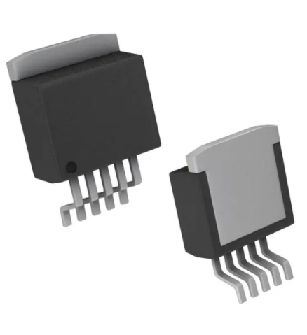


 工商网监
湘ICP备2023018690号
工商网监
湘ICP备2023018690号
