Product
Folder
Sample &
Buy
Technical
Documents
Support &
Community
Tools &
Software
LM2660
SNVS135E – SEPTEMBER 1999 – REVISED DECEMBER 2014
LM2660 Switched Capacitor Voltage Converter
1 Features
3 Description
•
•
•
•
•
•
The LM2660 CMOS charge-pump voltage converter
is a versatile unregulated switched capacitor inverter
or doubler. Operating from a wide 1.5-V to 5.5-V
supply voltage, the LM2660 uses two low-cost
capacitors to provide 100 mA of output current
without the cost, size and EMI related to inductorbased converters. With an operating current of only
120 µA and operating efficiency greater than 90% at
most loads, the LM2660 provides ideal performance
for battery-powered systems. LM2660 devices can be
operated directly in parallel to lower output
impedance, thus providing more current at a given
voltage.
1
Inverts or Doubles Input Supply Voltage
Narrow SOIC and VSSOP Packages
6.5-Ω Typical Output Resistance
88% Typical Conversion Efficiency at 100 mA
Selectable Oscillator Frequency: 10 kHz/80 kHz
Optional External Oscillator Input
2 Applications
•
•
•
•
•
•
Laptop Computers
Cellular Phones
Medical Instruments
Operational Amplifier Power Supplies
Interface Power Supplies
Handheld Instruments
space
space
space
space
The FC (frequency control) pin selects between a
nominal 10-kHz or 80-kHz oscillator frequency. The
oscillator frequency can be lowered by adding an
external capacitor to the OSC pin. Also, the OSC pin
may be used to drive the LM2660 with an external
clock up to 150 kHz. Through these methods, output
ripple frequency and harmonics may be controlled.
Additionally, the LM2660 may be configured to divide
a positive input voltage precisely in half. In this mode,
input voltages as high as 11 V may be used.
Device Information(1)
PART NUMBER
LM2660
PACKAGE
BODY SIZE (NOM)
SOIC (8)
4.90 mm x 3.91 mm
VSSOP (8)
3.00 mm x 3.00 mm
(1) For all available packages, see the orderable addendum at
the end of the datasheet.
Simplified Schematic
1
An IMPORTANT NOTICE at the end of this data sheet addresses availability, warranty, changes, use in safety-critical applications,
intellectual property matters and other important disclaimers. PRODUCTION DATA.
�LM2660
SNVS135E – SEPTEMBER 1999 – REVISED DECEMBER 2014
www.ti.com
Table of Contents
1
2
3
4
5
6
Features ..................................................................
Applications ...........................................................
Description .............................................................
Revision History.....................................................
Pin Configuration and Functions .........................
Specifications.........................................................
1
1
1
2
3
4
6.1
6.2
6.3
6.4
6.5
6.6
4
4
4
4
5
6
Absolute Maximum Ratings ......................................
Handling Ratings.......................................................
Recommended Operating Conditions.......................
Thermal Information ..................................................
Electrical Characteristics...........................................
Typical Characteristics ..............................................
7
Parameter Measurement Information .................. 8
8
Detailed Description .............................................. 9
7.1 Test Circuits .............................................................. 8
8.1 Overview ................................................................... 9
8.2 Functional Block Diagram ......................................... 9
8.3 Feature Description................................................... 9
8.4 Device Functional Modes........................................ 10
9
Application and Implementation ........................ 11
9.1 Application Information............................................ 11
9.2 Typical Applications ............................................... 11
10 Power Supply Recommendations ..................... 16
11 Layout................................................................... 17
11.1 Layout Guidelines ................................................. 17
11.2 Layout Example .................................................... 17
12 Device and Documentation Support ................. 18
12.1
12.2
12.3
12.4
Device Support ....................................................
Trademarks ...........................................................
Electrostatic Discharge Caution ............................
Glossary ................................................................
18
18
18
18
13 Mechanical, Packaging, and Orderable
Information ........................................................... 19
4 Revision History
NOTE: Page numbers for previous revisions may differ from page numbers in the current version.
Changes from Revision D (May 2013) to Revision E
•
Added Device Information and Handling Rating tables, Feature Description, Device Functional Modes, Application
and Implementation, Power Supply Recommendations, Layout, Device and Documentation Support, and
Mechanical, Packaging, and Orderable Information sections; moved some curves to Application Curves section ............. 1
Changes from Revision C (May 2013) to Revision D
•
2
Page
Page
Changed layout of National Data Sheet to TI format ........................................................................................................... 15
Submit Documentation Feedback
Copyright © 1999–2014, Texas Instruments Incorporated
Product Folder Links: LM2660
�LM2660
www.ti.com
SNVS135E – SEPTEMBER 1999 – REVISED DECEMBER 2014
5 Pin Configuration and Functions
SOIC (D) and VSSOP (DGK)
8 Pins
Top View
Pin Functions
PIN
NUMBER
NAME
DESCRIPTION
TYPE
VOLTAGE INVERTER
VOLTAGE DOUBLER
Frequency control for internal oscillator:
FC = open, fOSC = 10 kHz (typ);
1
FC
Input
FC = V+, fOSC = 80 kHz (typ);
Same as inverter.
FC has no effect when OSC pin is driven
externally.
2
CAP+
Power
Connect this pin to the positive terminal of chargeSame as inverter.
pump capacitor.
3
GND
Ground
Power supply ground input.
Power supply positive voltage input.
4
CAP−
Power
Connect this pin to the negative terminal of
charge-pump capacitor.
Same as inverter.
5
OUT
Power
Negative voltage output.
Power supply ground input.
LV must be tied to OUT.
6
LV
Input
Low-voltage operation input. Tie LV to GND when
input voltage is less than 3.5 V. Above 3.5 V, LV
can be connected to GND or left open. When
driving OSC with an external clock, LV must be
connected to GND.
7
OSC
Input
Oscillator control input. OSC is connected to an
internal 15-pF capacitor. An external capacitor can Same as inverter except that OSC cannot be
be connected to slow the oscillator. Also, an
driven by an external clock.
external clock can be used to drive OSC.
8
V+
Power
Power supply positive voltage input.
Positive voltage output.
Submit Documentation Feedback
Copyright © 1999–2014, Texas Instruments Incorporated
Product Folder Links: LM2660
3
�LM2660
SNVS135E – SEPTEMBER 1999 – REVISED DECEMBER 2014
www.ti.com
6 Specifications
6.1 Absolute Maximum Ratings
over operating free-air temperature range (unless otherwise noted) (1)
MIN
Supply voltage (V+ to GND, or GND to OUT)
MAX
UNIT
6
V
LV
(OUT − 0.3 V) to (GND +
3 V)
V
FC, OSC
The least negative of
(OUT − 0.3 V)
or (V+ − 6 V) to (V+ + 0.3
V)
V
V+ and OUT continuous output current
Output short-circuit duration to GND
(2)
120
mA
1
second
Power dissipation SOIC (D) (3)
735
mW
Power dissipation VSSOP (DGK) (3)
500
mW
300
°C
85
°C
Lead temperature (soldering, 10 seconds)
Operating junction temperature
(1)
(2)
(3)
–40
Stresses beyond those listed under Absolute Maximum Ratings may cause permanent damage to the device. These are stress ratings
only, which do not imply functional operation of the device at these or any other conditions beyond those indicated under Recommended
Operating Conditions. Exposure to absolute-maximum-rated conditions for extended periods may affect device reliability.
OUT may be shorted to GND for one second without damage. However, shorting OUT to V+ may damage the device and should be
avoided. Also, for temperatures above 85°C, OUT must not be shorted to GND or V+, or device may be damaged.
The maximum allowable power dissipation is calculated by using PDMax = (TJMax − TA)/RθJA, where TJMax is the maximum junction
temperature, TA is the ambient temperature, and RθJA is the junction-to-ambient thermal resistance of the specified package.
6.2 Handling Ratings
Tstg
Storage temperature range
V(ESD)
Electrostatic
discharge
(1)
MIN
MAX
UNIT
–65
150
°C
Human body model (HBM), per ANSI/ESDA/JEDEC JS-001, all pins (1)
2000
V
JEDEC document JEP155 states that 500-V HBM allows safe manufacturing with a standard ESD control process.
6.3 Recommended Operating Conditions
over operating free-air temperature range (unless otherwise noted)
MIN
V+ (supply voltage)
NOM
MAX
Inverter, LV = Open
3.5
5.5
Inverter, LV = GND
1.5
5.5
Doubler, LV = OUT
2.5
5.5
–40
85
Junction temperature (TJ)
UNIT
°C
6.4 Thermal Information
LM2660
THERMAL METRIC
RθJA
(1)
4
(1)
Junction-to-ambient thermal resistance
SOIC (D)
VSSOP (DGK)
8 PINS
8 PINS
170
250
UNIT
°C/W
For more information about traditional and new thermal metrics, see the IC Package Thermal Metrics application report, SPRA953.
Submit Documentation Feedback
Copyright © 1999–2014, Texas Instruments Incorporated
Product Folder Links: LM2660
�LM2660
www.ti.com
SNVS135E – SEPTEMBER 1999 – REVISED DECEMBER 2014
6.5 Electrical Characteristics
Limits in for typical (TYP) values are for TJ = 25°C, and limits in for minimum (MIN) and maximum (MAX) values apply over
the full operating temperature range; V+ = 5V, FC = Open, C1 = C2 = 150 μF, unless otherwise specified in the Test
Conditions. (1)
PARAMETER
V+
Supply voltage
TEST CONDITIONS
RL = 1k
ROUT
Output resistance (2)
IL = 100 mA
fOSC
Oscillator frequency
OSC = Open
fSW
Switching frequency (3)
OSC = Open
IOSC
OSC input current
Power efficiency
1.5
5.5
Doubler, LV = OUT
2.5
FC = V+
Output current
PEFF
Inverter, LV = GND
LV = Open
IL
TA ≤ 85°C, OUT ≤ −4 V
100
TA > 85°C, OUT ≤ −3.8 V
100
TA ≤ 85°C
FC = Open
(1)
(2)
(3)
0.5
1
3
10
12
5
10
FC = V+
40
80
FC = Open
2.5
5
FC = V+
20
40
±2
FC = V+
±16
RL (1k) between V+ and OUT
96%
98%
RL (500) between GND and OUT
92%
96%
99%
99.96%
Voltage conversion efficiency No Load
V
mA
mA
6.5
FC = Open
UNIT
5.5
0.12
TA > 85°C
IL = 100 mA to GND
VOEFF
MAX
5.5
FC = Open
Supply current
TYP
3.5
No Load
IQ
MIN
Inverter, LV = Open
Ω
kHz
kHz
µA
88%
In the test circuit, capacitors C1 and C2 are 0.2-Ω maximum ESR capacitors. Capacitors with higher ESR will increase output resistance,
reduce output voltage and efficiency.
Specified output resistance includes internal switch resistance and capacitor ESR.
The output switches operate at one half of the oscillator frequency, fOSC = 2fSW.
Submit Documentation Feedback
Copyright © 1999–2014, Texas Instruments Incorporated
Product Folder Links: LM2660
5
�LM2660
SNVS135E – SEPTEMBER 1999 – REVISED DECEMBER 2014
www.ti.com
6.6 Typical Characteristics
(Circuit of Figure 12)
6
Figure 1. Supply Current vs Supply Voltage
Figure 2. Supply Current vs Oscillator Frequency
Figure 3. Output Source Resistance vs Supply Voltage
Figure 4. Output Source Resistance vs Temperature
Figure 5. Output Voltage Drop vs Load Current
Figure 6. Output Voltage vs Oscillator Frequency
Submit Documentation Feedback
Copyright © 1999–2014, Texas Instruments Incorporated
Product Folder Links: LM2660
�LM2660
www.ti.com
SNVS135E – SEPTEMBER 1999 – REVISED DECEMBER 2014
Typical Characteristics (continued)
(Circuit of Figure 12)
Figure 7. Oscillator Frequency vs External Capacitance
Figure 8. Oscillator Frequency vs Supply Voltage
(Fc = V+)
Figure 9. Oscillator Frequency vs Supply Voltage
(Fc = Open)
Figure 10. Oscillator Frequency vs Temperature
(Fc = V+)
Figure 11. Oscillator Frequency vs Temperature
(Fc = Open)
Submit Documentation Feedback
Copyright © 1999–2014, Texas Instruments Incorporated
Product Folder Links: LM2660
7
�LM2660
SNVS135E – SEPTEMBER 1999 – REVISED DECEMBER 2014
www.ti.com
7 Parameter Measurement Information
7.1 Test Circuits
Figure 12. LM2660 Test Circuit
8
Submit Documentation Feedback
Copyright © 1999–2014, Texas Instruments Incorporated
Product Folder Links: LM2660
�LM2660
www.ti.com
SNVS135E – SEPTEMBER 1999 – REVISED DECEMBER 2014
8 Detailed Description
8.1 Overview
The LM2660 contains four large CMOS switches which are switched in a sequence to invert the input supply
voltage. Energy transfer and storage are provided by external capacitors. Figure 13 illustrates the voltage
conversion scheme. When S1 and S3 are closed, C1 charges to the supply voltage V+. During this time interval
switches S2 and S4 are open. In the second time interval, S1 and S3 are open and S2 and S4 are closed, C1 is
charging C2. After a number of cycles, the voltage across C2 will be pumped to V+. Since the anode of C2 is
connected to ground, the output at the cathode of C2 equals −(V+) assuming no load on C2, no loss in the
switches, and no ESR in the capacitors. In reality, the charge transfer efficiency depends on the switching
frequency, the on-resistance of the switches, and the ESR of the capacitors.
Figure 13. Voltage Inverting Principle
8.2 Functional Block Diagram
LM2660
V+
OUT
FC
OSCILLATOR
OSC
Switch Array
Switch Drivers
LV
CAP+
CAPGND
8.3 Feature Description
8.3.1 Changing Oscillator Frequency
The internal oscillator frequency can be selected using the Frequency Control (FC) pin. When FC is open, the
oscillator frequency is 10 kHz; when FC is connected to V+, the frequency increases to 80 kHz. A higher
oscillator frequency allows smaller capacitors to be used for equivalent output resistance and ripple, but
increases the typical supply current from 0.12 mA to 1 mA.
The oscillator frequency can be lowered by adding an external capacitor between OSC and GND. (See Typical
Characteristics.) Also, in the inverter mode, an external clock that swings within 100 mV of V+ and GND can be
used to drive OSC. Any CMOS logic gate is suitable for driving OSC. LV must be grounded when driving OSC.
The maximum external clock frequency is limited to 150 kHz.
The switching frequency of the converter (also called the charge pump frequency) is half of the oscillator
frequency.
NOTE
OSC cannot be driven by an external clock in the voltage-doubling mode.
Submit Documentation Feedback
Copyright © 1999–2014, Texas Instruments Incorporated
Product Folder Links: LM2660
9
�LM2660
SNVS135E – SEPTEMBER 1999 – REVISED DECEMBER 2014
www.ti.com
Feature Description (continued)
Table 1. LM2660 Oscillator Frequency Selection
FC
OSC
OSCILLATOR
Open
Open
10 kHz
V+
Open
80 kHz
Open or V+
External Capacitor
See Typical Characteristics
N/A
External Clock
External Clock
(inverter mode only)
Frequency
8.4 Device Functional Modes
When V+ is applied to the LM2660, the device becomes enabled and will operate in which ever configuration the
device is placed (inverter, doubler, etc.).
10
Submit Documentation Feedback
Copyright © 1999–2014, Texas Instruments Incorporated
Product Folder Links: LM2660
�LM2660
www.ti.com
SNVS135E – SEPTEMBER 1999 – REVISED DECEMBER 2014
9 Application and Implementation
NOTE
Information in the following applications sections is not part of the TI component
specification, and TI does not warrant its accuracy or completeness. TI’s customers are
responsible for determining suitability of components for their purposes. Customers should
validate and test their design implementation to confirm system functionality.
9.1 Application Information
The LM2660 CMOS charge-pump voltage converter is a versatile unregulated switched capacitor inverter or
doubler. Operating from a wide 1.5 V to 5.5 V supply voltage, the LM2660 uses two low-cost capacitors to
provide 100 mA of output current without the cost, size and EMI related to inductor-based converters. With an
operating current of only 120 µA and operating efficiency greater than 90% at most loads, the LM2660 provides
ideal performance for battery-powered systems. LM2660 devices can be operated directly in parallel to lower
output impedance, thus providing more current at a given voltage.
9.2 Typical Applications
9.2.1 Voltage Inverter
Figure 14. LM2660 Voltage Inverter
9.2.1.1 Design Requirements
The main application of LM2660 is to generate a negative supply voltage. The voltage inverter circuit uses only
two external capacitors as shown in the Figure 14. The range of the input supply voltage is 1.5 V to 5.5 V. For a
supply voltage less than 3.5V, the LV pin must be connected to ground to bypass the internal regulator circuitry.
This gives the best performance in low voltage applications. If the supply voltage is greater than 3.5 V, LV may
be connected to ground or left open. The choice of leaving LV open simplifies the direct substitution of the
LM2660 for the LMC7660 Switched Capacitor Voltage Converter.
9.2.1.2 Detailed Design Procedure
The output characteristics of this circuit can be approximated by an ideal voltage source in series with a resistor.
The voltage source equals −(V+). The output resistance Rout is a function of the ON resistance of the internal
MOS switches, the oscillator frequency, and the capacitance and ESR of C1 and C2. A good approximation is:
where
•
RSW is the sum of the ON resistance of the internal MOS switches shown in Figure 13.
(1)
High value, low ESR capacitors will reduce the output resistance. Instead of increasing the capacitance, the
oscillator frequency can be increased to reduce the 2/(fosc × C1) term. Once this term is trivial compared with RSW
and ESRs, further increasing in oscillator frequency and capacitance will become ineffective.
The peak-to-peak output voltage ripple is determined by the oscillator frequency, and the capacitance and ESR
of the output capacitor C2:
(2)
Again, using a low ESR capacitor will result in lower ripple.
Submit Documentation Feedback
Copyright © 1999–2014, Texas Instruments Incorporated
Product Folder Links: LM2660
11
�LM2660
SNVS135E – SEPTEMBER 1999 – REVISED DECEMBER 2014
www.ti.com
Typical Applications (continued)
9.2.1.2.1 Capacitor Selection
The output resistance and ripple voltage are dependent on the capacitance and ESR values of the external
capacitors. The output voltage drop is the load current times the output resistance, and the power efficiency is
where
•
•
IQ(V+) is the quiescent power loss of the IC device, and
IL2ROUT is the conversion loss associated with the switch on-resistance, the two external capacitors and their
ESRs.
(3)
Since the switching current charging and discharging C1 is approximately twice as the output current, the effect
of the ESR of the pumping capacitor C1 is multiplied by four in the output resistance. The output capacitor C2 is
charging and discharging at a current approximately equal to the output current, therefore, its ESR only counts
once in the output resistance. However, the ESR of C2 directly affects the output voltage ripple. Therefore, low
ESR capacitors (Table 2) are recommended for both capacitors to maximize efficiency, reduce the output voltage
drop and voltage ripple. For convenience, C1 and C2 are usually chosen to be the same.
The output resistance varies with the oscillator frequency and the capacitors. In Figure 15, the output resistance
vs. oscillator frequency curves are drawn for three different tantalum capacitors. At very low frequency range,
capacitance plays the most important role in determining the output resistance. Once the frequency is increased
to some point (such as 20 kHz for the 150 μF capacitors), the output resistance is dominated by the ON
resistance of the internal switches and the ESRs of the external capacitors. A low value, smaller size capacitor
usually has a higher ESR compared with a bigger size capacitor of the same type. For lower ESR, use ceramic
capacitors.
Figure 15. Output Source Resistance vs Oscillator Frequency
Table 2. Low ESR Capacitor Manufacturers
MANUFACTURER
CAPACITOR TYPE
Nichicon Corp.
PL, PF series, through-hole aluminum electrolytic
AVX Corp.
TPS series, surface-mount tantalum
Sprague
593D, 594D, 595D series, surface-mount tantalum
Sanyo
OS-CON series, through-hole aluminum electrolytic
12
Submit Documentation Feedback
Copyright © 1999–2014, Texas Instruments Incorporated
Product Folder Links: LM2660
�LM2660
www.ti.com
SNVS135E – SEPTEMBER 1999 – REVISED DECEMBER 2014
9.2.1.2.2 Paralleling Devices
Any number of LM2660s can be paralleled to reduce the output resistance. Each device must have its own
pumping capacitor C1, while only one output capacitor Cout is needed as shown in Figure 16. The composite
output resistance is:
Rout =
Rout of each LM2660
Number of Devices
(4)
Figure 16. Lowering Output Resistance By Paralleling Devices
9.2.1.2.3 Cascading Devices
Cascading the LM2660s is an easy way to produce a greater negative voltage (as shown in Figure 17). If n is the
integer representing the number of devices cascaded, the unloaded output voltage Vout is (−nVin). The effective
output resistance is equal to the weighted sum of each individual device:
(5)
A three-stage cascade circuit shown in Figure 18 generates −3 Vin, from Vin.
Cascading is also possible when devices are operating in doubling mode. In Figure 19, two devices are
cascaded to generate 3 Vin.
An example of using the circuit in Figure 18 or Figure 19 is generating +15 V or −15 V from a +5 V input.
Note that, the number of n is practically limited since the increasing of n significantly reduces the efficiency and
increases the output resistance and output voltage ripple.
Figure 17. Increasing Output Voltage by Cascading Devices
Submit Documentation Feedback
Copyright © 1999–2014, Texas Instruments Incorporated
Product Folder Links: LM2660
13
�LM2660
SNVS135E – SEPTEMBER 1999 – REVISED DECEMBER 2014
www.ti.com
Figure 18. Generating −3VIN from +VIN
Figure 19. Generating +3VIN from +VIN
9.2.1.2.4 Regulating VOUT
It is possible to regulate the output of the LM2660 by use of a low dropout regulator (such as LP2951). The
whole converter is depicted in Figure 20. This converter can give a regulated output from −1.5 V to −5.5 V by
choosing the proper resistor ratio:
where
•
Vref = 1.235 V
(6)
The error flag on pin 5 of the LP2951 goes low when the regulated output at pin 4 drops by about 5%. The
LP2951 can be shutdown by taking pin 3 high.
Figure 20. Combining LM2660 With LP2951 to Make a Negative Adjustable Regulator
14
Submit Documentation Feedback
Copyright © 1999–2014, Texas Instruments Incorporated
Product Folder Links: LM2660
�LM2660
www.ti.com
SNVS135E – SEPTEMBER 1999 – REVISED DECEMBER 2014
Also, as shown in Figure 21 by operating LM2660 in voltage doubling mode and adding a linear regulator (such
as LP2981) at the output, we can get +5 V output from an input as low as +3 V.
Figure 21. Generating +5 V from +3 V Input Voltage
9.2.1.3 Application Curves
Figure 22. Efficiency vs Load Current
Figure 23. Efficiency vs Oscillator Frequency
9.2.2 Positive Voltage Doubler
Figure 24. LM2660 Voltage Doubler
9.2.2.1 Design Requirements
The LM2660 can operate as a positive voltage doubler (as shown in the Figure 24). The doubling function is
achieved by reversing some of the connections to the device. The input voltage is applied to the GND pin with an
allowable voltage from 2.5 V to 5.5 V. The V+ pin is used as the output. The LV pin and OUT pin must be
connected to ground. The OSC pin can not be driven by an external clock in this operation mode. The unloaded
output voltage is twice of the input voltage and is not reduced by the diode D1's forward drop.
Submit Documentation Feedback
Copyright © 1999–2014, Texas Instruments Incorporated
Product Folder Links: LM2660
15
�LM2660
SNVS135E – SEPTEMBER 1999 – REVISED DECEMBER 2014
www.ti.com
9.2.2.2 Detailed Design Procedure
The Schottky diode D1 is only needed for start-up. The internal oscillator circuit uses the V+ pin and the LV
pin (connected to ground in the voltage doubler circuit) as its power rails. Voltage across V+ and LV must be
larger than 1.5 V to insure the operation of the oscillator. During start-up, D1 is used to charge up the voltage
at V+ pin to start the oscillator; also, it protects the device from turning-on its own parasitic diode and
potentially latching-up. Therefore, the Schottky diode D1 should have enough current carrying capability to
charge the output capacitor at start-up, as well as a low forward voltage to prevent the internal parasitic
diode from turning-on. A Schottky diode like 1N5817 can be used for most applications. If the input voltage
ramp is less than 10V/ms, a smaller Schottky diode like MBR0520LT1 can be used to reduce the circuit size.
9.2.2.3 Application Curves
See Application Curves in the Voltage Inverter section.
10 Power Supply Recommendations
The LM2660 is designed to operate from as an inverter over an input voltage supply range between 1.5 V and
5.5 V when the LV pin is grounded. This input supply must be well regulated and capable to supply the required
input current. If the input supply is located far from the LM2660 additional bulk capacitance may be required in
addition to the ceramic bypass capacitors.
16
Submit Documentation Feedback
Copyright © 1999–2014, Texas Instruments Incorporated
Product Folder Links: LM2660
�LM2660
www.ti.com
SNVS135E – SEPTEMBER 1999 – REVISED DECEMBER 2014
11 Layout
11.1 Layout Guidelines
The high switching frequency and large switching currents of the LM2660 make the choice of layout important.
The following steps should be used as a reference to ensure the device is stable and maintains proper LED
current regulation across its intended operating voltage and current range:
• Place CIN on the top layer (same layer as the LM2660) and as close to the device as possible. Connecting
the input capacitor through short, wide traces to both the V+ and GND pins reduces the inductive voltage
spikes that occur during switching which can corrupt the V+ line.
• Place COUT on the top layer (same layer as the LM2660) and as close as possible to the OUT and GND pin.
The returns for both CIN and COUT should come together at one point, as close to the GND pin as possible.
Connecting COUT through short, wide traces reduce the series inductance on the OUT and GND pins that can
corrupt the VOUT and GND lines and cause excessive noise in the device and surrounding circuitry.
• Place C1 on the top layer (same layer as the LM2660) and as close to the device as possible. Connect the
flying capacitor through short, wide traces to both the CAP+ and CAP– pins.
11.2 Layout Example
LM2660
FC
CAP+
V+
OSC
GND
LV
CAP-
OUT
Figure 25. LM2660 Layout Example
Submit Documentation Feedback
Copyright © 1999–2014, Texas Instruments Incorporated
Product Folder Links: LM2660
17
�LM2660
SNVS135E – SEPTEMBER 1999 – REVISED DECEMBER 2014
www.ti.com
12 Device and Documentation Support
12.1 Device Support
12.1.1 Third-Party Products Disclaimer
TI'S PUBLICATION OF INFORMATION REGARDING THIRD-PARTY PRODUCTS OR SERVICES DOES NOT
CONSTITUTE AN ENDORSEMENT REGARDING THE SUITABILITY OF SUCH PRODUCTS OR SERVICES
OR A WARRANTY, REPRESENTATION OR ENDORSEMENT OF SUCH PRODUCTS OR SERVICES, EITHER
ALONE OR IN COMBINATION WITH ANY TI PRODUCT OR SERVICE.
12.2 Trademarks
All trademarks are the property of their respective owners.
12.3 Electrostatic Discharge Caution
These devices have limited built-in ESD protection. The leads should be shorted together or the device placed in conductive foam
during storage or handling to prevent electrostatic damage to the MOS gates.
12.4 Glossary
SLYZ022 — TI Glossary.
This glossary lists and explains terms, acronyms, and definitions.
18
Submit Documentation Feedback
Copyright © 1999–2014, Texas Instruments Incorporated
Product Folder Links: LM2660
�LM2660
www.ti.com
SNVS135E – SEPTEMBER 1999 – REVISED DECEMBER 2014
13 Mechanical, Packaging, and Orderable Information
The following pages include mechanical, packaging, and orderable information. This information is the most
current data available for the designated devices. This data is subject to change without notice and revision of
this document. For browser-based versions of this data sheet, refer to the left-hand navigation.
Submit Documentation Feedback
Copyright © 1999–2014, Texas Instruments Incorporated
Product Folder Links: LM2660
19
�PACKAGE OPTION ADDENDUM
www.ti.com
30-Sep-2021
PACKAGING INFORMATION
Orderable Device
Status
(1)
Package Type Package Pins Package
Drawing
Qty
Eco Plan
(2)
Lead finish/
Ball material
MSL Peak Temp
Op Temp (°C)
Device Marking
(3)
(4/5)
(6)
LM2660-MWC
ACTIVE
WAFERSALE
YS
0
1
RoHS & Green
Call TI
Level-1-NA-UNLIM
-40 to 85
LM2660M
NRND
SOIC
D
8
95
Non-RoHS
& Green
Call TI
Level-1-235C-UNLIM
-40 to 85
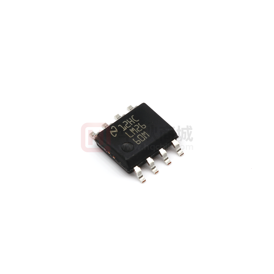
LM26
60M
LM2660M/NOPB
ACTIVE
SOIC
D
8
95
RoHS & Green
SN
Level-1-260C-UNLIM
-40 to 85
LM26
60M
LM2660MM/NOPB
ACTIVE
VSSOP
DGK
8
1000
RoHS & Green
SN
Level-1-260C-UNLIM
-40 to 85
S01A
LM2660MX/NOPB
ACTIVE
SOIC
D
8
2500
RoHS & Green
SN
Level-1-260C-UNLIM
-40 to 85
LM26
60M
(1)
The marketing status values are defined as follows:
ACTIVE: Product device recommended for new designs.
LIFEBUY: TI has announced that the device will be discontinued, and a lifetime-buy period is in effect.
NRND: Not recommended for new designs. Device is in production to support existing customers, but TI does not recommend using this part in a new design.
PREVIEW: Device has been announced but is not in production. Samples may or may not be available.
OBSOLETE: TI has discontinued the production of the device.
(2)
RoHS: TI defines "RoHS" to mean semiconductor products that are compliant with the current EU RoHS requirements for all 10 RoHS substances, including the requirement that RoHS substance
do not exceed 0.1% by weight in homogeneous materials. Where designed to be soldered at high temperatures, "RoHS" products are suitable for use in specified lead-free processes. TI may
reference these types of products as "Pb-Free".
RoHS Exempt: TI defines "RoHS Exempt" to mean products that contain lead but are compliant with EU RoHS pursuant to a specific EU RoHS exemption.
Green: TI defines "Green" to mean the content of Chlorine (Cl) and Bromine (Br) based flame retardants meet JS709B low halogen requirements of


 工商网监
湘ICP备2023018690号
工商网监
湘ICP备2023018690号

