LM2687
LM2687 Low Noise Regulated Switched Capacitor Voltage Inverter
Literature Number: SNVS060D
�LM2687
Low Noise Regulated Switched Capacitor Voltage
Inverter
General Description
Features
The LM2687 CMOS Negative Regulated Switched Capacitor
Voltage Inverter delivers a very low noise adjustable output
for an input voltage in the range of +2.7V to +5.5V. Four low
cost capacitors are used in this circuit to provide up to 10mA
of output current. The regulated output for the LM2687 is
adjustable between −1.5V and −5.2V. The LM2687 operates
at 100 kHz (typical) switching frequency to reduce output
resistance and voltage ripple. With an operating current of
only 500 µA (charge pump power efficiency greater than
90% with most loads) and 0.05 µA typical shutdown current,
the LM2687 provides ideal performance for cellular phone
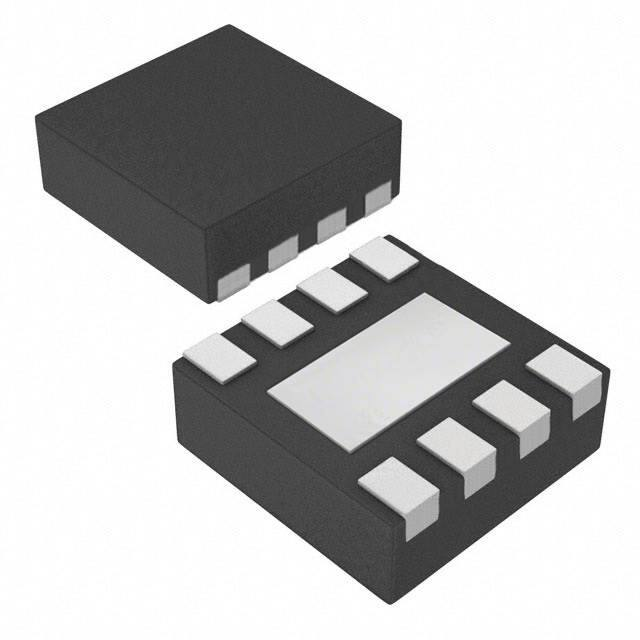
power amplifier bias and other low current, low noise negative voltage needs. The device comes in a small 8-pin MSOP
or LLP package.
n
n
n
n
n
Inverts and regulates the input supply voltage
Small MSOP-8 or LLP-8 package
91% typical charge pump power efficiency at 10mA
Low output ripple (1mV typical)
Shutdown lowers Quiescent current to 0.05 µA (typical)
Applications
n
n
n
n
n
Wireless Communication Systems
Cellular Phone Power Amplifier Biasing
Interface Power Supplies
Handheld Instrumentation
Laptop Computers and PDA’s
Typical Application Circuit
10118001
Connection Diagrams
8-Pin MSOP
8-Pin LLP
10118002
10118025
© 2003 National Semiconductor Corporation
DS101180
www.national.com
LM2687 Low Noise Regulated Switched Capacitor Voltage Inverter
April 2003
�LM2687
Ordering Information for MSOP Package
Device Order Number
Package Number
Package Marking*
LM2687MM
MUA08A
S12A
Tape and Reel (1000 units/reel)
LM2687MMX
MUA08A
S12A
Tape and Reel (3500 units/reel)
Supplies As
Ordering Information for LLP Package
Device Order Number
Package Number
Package Marking*
LM2687LD
LDA08A
L050B
Tape and Reel (1000 units/reel)
LM2687LDX
LDA08A
L050B
Tape and Reel (3500 units/reel)
Supplies As
Note: * The small physical sizes of the MSOP-8 and LLP-8 packages do not
allow for the full part number marking. Devices will be marked with the
designation shown in the column Package Marking.
Pin Description
Pin No.
Name
1
Cap+
Positive terminal for C1.
2
GND
Ground.
3
Cap−
Negative terminal for C1.
4
SD
Active low, logic-level shutdown input.
5
VNEG
Negative unregulated output voltage.
6
VFB
7
VOUT
8
VIN
DAP
Die Attach Pad
www.national.com
Function
Feedback input. Connect VFB to an external resistor divider between VOUT and a positive
adjust voltage VADJ (0≤VADJ≤VIN). DO NOT leave unconnected.
Regulated negative output voltage.
Positive power supply input.
LLP package only. Connect this pad to VNEG.
2
�TJMAX (Note 3)
(Note 1)
θJA (Note 3)
If Military/Aerospace specified devices are required,
please contact the National Semiconductor Sales Office/
Distributors for availability and specifications.
Supply Voltage (VIN to GND or GND
to OUT)
150˚C
250˚C/W
Operating Input Voltage Range
2.7V to 5.5V
Operating Output Current Range
Operating Ambient
+ 5.8V
Temp. Range
(GND − 0.3V) to
(VIN + 0.3V)
SD
VNEG and VOUT Continuous Output
Current
10mA
VOUT Short-Circuit Duration to GND
(Note 2)
1 sec.
Continuous Power Dissipation (TA =
25˚C) (Note 3)
600mW
0mA to 10mA
−40˚C to 85˚C
Operating Junction Temp. Range
−40˚C to 110˚C
Storage Temperature
−65˚C to 150˚C
Lead Temp. (Soldering, 10 sec.)
300˚C
ESD Rating (Note 4)
2kV
Electrical Characteristics
Limits with standard typeface apply for TJ = 25˚C, and limits in boldface type apply over the full temperature range. Unless
otherwise specified VIN = 3.6V, C1 = C2 = 1µF, C3 = 10µF.
Symbol
Parameter
Conditions
Min
Typ
Max
500
950
µA
0.05
1
µA
110
105
180
170
kHz
IQ
Supply Current
ISD
Shutdown Supply Current
FSW
Switching Frequency
(Note 5)
2.7V ≤ VIN ≤.5.5V
VIN = 3.6V
ηPOWER
Power Efficiency at VNEG
IL = 3.6mA
IL = 10mA
94
91
TSTART
Start Up time
(Note 6)
120
Open Circuit, No Load
50
60
Units
%
600
µs
Output Resistance to VNEG
(Note 7)
30
Ω
VR
Output Voltage Ripple
(Note 8)
IL =2.5mA, VOUT = −2.7V
IL = 10mA, VOUT = −3.8V
1
2
mV
VFB
Feedback Pin Reference
Voltage
IL = 2.5mA (Note 9)
Adjustable Output Voltage
5.5V ≥ VIN ≥ 2.7V, 2.5mA ≥ IL
5.5V ≥ VIN ≥ 3.0V, 10mA ≥ IL ≥
0mA
Load Regulation
0 to 10mA, VOUT = − 2.4V
5
mV/mA
Line Regulation
5.5V ≥ VIN ≥ 2.7V, IL = 2.5mA
1
mV/V
RNEG
VOUT
VIH
Shutdown Pin Input Voltage 5.5V ≥ VIN ≥ 2.7V
High
VIL
Shutdown Pin Input Voltage 5.5V ≥ VIN ≥ 2.7V
Low
−1.25
−1.20
−1.15
V
V
− (VIN −0.3V)
− (VIN −1.2V)
2.2
V
0.5
V
Note 1: Absolute Maximum Ratings indicate limits beyond which damage to the device may occur. Electrical specifications do not apply when operating the device
beyond its rated operating conditions.
Note 2: OUT may be shorted to GND for one second without damage. However, shorting OUT to VIN may damage the device and must be avoided. Also, for
temperatures above TA = 85˚C, OUT must not be shorted to GND or VIN or device may be damaged.
Note 3: The maximum power dissipation must be de-rated at elevated temperatures and is limited by TJMAX (maximum junction temperature), TA (ambient
temperature) and θJA (junction-to-ambient thermal resistance). The maximum power dissipation at any temperature is:
PDissMAX = (TJMAX — TA)/θJA up to the value listed in the Absolute Maximum Ratings.
Note 4: Rating is for the human body model, a 100pF capacitor discharged through a 1.5 kΩ resistor into each pin.
Note 5: The output switches operate at one half the oscillator frequency, fOSC = 2fSW.
Note 6: All capacitors are 1µF.
Note 7: Current drawn from VNEG pin decreases power efficiency and will increase output voltage ripple.
Note 8: In the test circuit, capacitors C1 and C2 are 1µF, C3 = 10µF, 0.30Ω maximum ESR capacitors. Capacitors with higher ESR will increase output resistance,
increase output voltage ripple, and reduce efficiency.
Note 9: The feedback resistors R1 and R2 are 200kΩ resistors.
3
www.national.com
LM2687
Absolute Maximum Ratings
�LM2687
10118021
FIGURE 1. Standard Application Circuit for Minimum Capacitance Values
10118022
FIGURE 2. Standard Application Circuit for Low Output Noise
www.national.com
4
�Unless otherwise specified, TA = 25˚C, VOUT = −2.5V.
Output Voltage vs. Output Current
Figure 2
Output Voltage vs. Output Current
Figure 1
10118005
10118004
Output Voltage vs. Input Voltage
Maximum Output Current vs. Input Voltage
10118006
10118007
Maximum VNEG Current vs. Input Voltage
No Load Supply Current vs. Input Voltage
10118008
10118009
5
www.national.com
LM2687
Typical Performance Characteristics
�LM2687
Typical Performance Characteristics Unless otherwise specified, TA = 25˚C,
VOUT = −2.5V. (Continued)
Start-Up Time vs. Input Voltage
Figure 1
Switching Frequency vs. Input Voltage
10118010
10118011
Start-Up from Shutdown (no load)
Figure 2
Output Ripple
Figure 1
10118013
10118012
Output Ripple
Figure 2
Line Transient Response
10118017
10118014
www.national.com
6
�LM2687
Typical Performance Characteristics Unless otherwise specified, TA = 25˚C,
VOUT = −2.5V. (Continued)
Load Transient Response
VFB vs. Temperature
10118018
10118015
Output Noise Spectrum
Figure 1
Output Noise Spectrum
Figure 2
10118024
10118023
10118003
FIGURE 3. Functional Block Diagram
7
www.national.com
�LM2687
Device Description
The LM2687 is an inverting, regulated charge-pump power
converter. It features low noise, small physical size, and is
simple to use. It is an ideal solution for biasing GaAsFET
devices such as power amplifier modules found in portable
devices and cellular phones.
A switched capacitor charge-pump circuit is used to invert
the input voltage VIN to its corresponding negative value
which is seen at VNEG. This voltage is regulated by a low
dropout linear regulator at VOUT (Figure 3). The output voltage can be regulated anywhere from −1.5V to −5.2V and is
determined by a pair of feedback resistors (see Setting the
Output Voltage). The PSRR of the linear regulator reduces
the output voltage ripple produced by the charge-pump inverter to 1mVP-P (typical) at the output VOUT. The regulator
also attenuates noise from the incoming supply due to its
high PSRR.
The switching frequency is fixed at 100kHz and RSW (the
combined resistance of the internal switches) is typically
10Ω. It is clear from this equation that low ESR capacitors
are desirable and that larger values of C1 will further reduce
the output resistance. The output resistance of the entire
circuit (in dropout) is:
ROUT = RNEG + Rregulator
Rregulator (the output impedance of the linear regulator) is
approximately 10Ω. When the circuit is in regulation, the
overall output resistance is equal to the linear regulator load
regulation (5mV/mA). The dropout voltage is therefore affected by the capacitors used since it is simply defined as
IOUT*ROUT.
A larger value of capacitor and lower ESR for C2 will lower
the output voltage ripple of the charge-pump. This ripple will
then be subject to the PSRR of the linear regulator and
reduced at VOUT. A larger value and lower ESR for C3 will
further reduce this ripple.
Shutdown
The LM2687 features a logic-level shutdown feature. The
function is active-low and will reduce the supply current to
0.05µA (typical) when engaged. When shutdown is active
VOUT and VNEG are switched to ground.
The Low Dropout Linear Regulator uses an N-channel FET
device which behaves similarly to an NPN device. Because
of this and the internal compensation there are no strict ESR
requirements for the output capacitor to maintain stability.
Using the minimum recommended values will ensure stability under all conditions.
In summation, larger value capacitors with lower ESR will
give the lowest output noise and ripple. C1, C2, and C3
should be 1.0µF minimum with less than 0.3Ω ESR. Larger
values may be used for any or all capacitors. All capacitors
should be either ceramic, surface-mount chip tantalum, or
polymer electrolytic.
Application Information
SETTING THE OUTPUT VOLTAGE
The output voltage on the LM2687 is set by using a resistor
divider between the output, the feedback pin, and an arbitrary voltage VADJ (Figure 3). VADJ can range from GND to
any positive voltage up to VIN. VADJ is usually chosen to be
GND and should not be connected to a different voltage
unless it is well regulated so the output will stay constant.
The feedback pin is held at a constant voltage VFB which
equals −1.2V. The output voltage can be selected using the
equation:
OUTPUT NOISE AND RIPPLE
Low output noise and output voltage ripple are two of the
attractive features of the LM2687. Because they are small,
the noise and ripple (1mV typ.) can be hard to measure
accurately. Ground loop error between the circuit and the
oscilloscope caused by the switching of the charge-pump
produces ground currents in the probe wires. This causes
sharp voltage spikes on the oscilloscope waveform. To reduce this error measure, the output directly at the output
capacitor (C3) and use the shortest wires possible. Also, do
not use the ground lead on the probe. Take the tip cover off
of the probe and touch the grounding ring of the probe
directly to the ground terminal of C3. This should give the
most accurate reading of the actual output waveform.
The current into the feedback pin IFB is in the range of 10nA
to 100nA. Therefore using a value of 500kΩ or smaller for R1
should make this current of little concern when setting the
output voltage. For best accuracy, use resistors with 1% or
better tolerance.
CAPACITOR SELECTION
Selecting the right capacitors for your circuit is important.
The capacitors affect the output resistance of the chargepump, the output voltage ripple, and the overall dropout
voltage (VIN-|VOUT|) of the circuit. The output resistance of
the charge-pump inverter is:
www.national.com
8
�LM2687
Physical Dimensions
inches (millimeters) unless otherwise noted
MSOP-8 Package
8-Lead Mini SO-8 (MM)
For Ordering, Refer to Ordering Information Table
NS Package Number MUA08A
9
www.national.com
�LM2687 Low Noise Regulated Switched Capacitor Voltage Inverter
Physical Dimensions
inches (millimeters) unless otherwise noted (Continued)
LLP-8 Package
8-Lead Leadless Leadframe Package (LD)
For Ordering, Refer to Ordering Information Table
NS Package Number LDA08A
LIFE SUPPORT POLICY
NATIONAL’S PRODUCTS ARE NOT AUTHORIZED FOR USE AS CRITICAL COMPONENTS IN LIFE SUPPORT
DEVICES OR SYSTEMS WITHOUT THE EXPRESS WRITTEN APPROVAL OF THE PRESIDENT AND GENERAL
COUNSEL OF NATIONAL SEMICONDUCTOR CORPORATION. As used herein:
1. Life support devices or systems are devices or
systems which, (a) are intended for surgical implant
into the body, or (b) support or sustain life, and
whose failure to perform when properly used in
accordance with instructions for use provided in the
labeling, can be reasonably expected to result in a
significant injury to the user.
National Semiconductor
Americas Customer
Support Center
Email: new.feedback@nsc.com
Tel: 1-800-272-9959
www.national.com
National Semiconductor
Europe Customer Support Center
Fax: +49 (0) 180-530 85 86
Email: europe.support@nsc.com
Deutsch Tel: +49 (0) 69 9508 6208
English Tel: +44 (0) 870 24 0 2171
Français Tel: +33 (0) 1 41 91 8790
2. A critical component is any component of a life
support device or system whose failure to perform
can be reasonably expected to cause the failure of
the life support device or system, or to affect its
safety or effectiveness.
National Semiconductor
Asia Pacific Customer
Support Center
Fax: +65-6250 4466
Email: ap.support@nsc.com
Tel: +65-6254 4466
National Semiconductor
Japan Customer Support Center
Fax: 81-3-5639-7507
Email: jpn.feedback@nsc.com
Tel: 81-3-5639-7560
National does not assume any responsibility for use of any circuitry described, no circuit patent licenses are implied and National reserves the right at any time without notice to change said circuitry and specifications.
�IMPORTANT NOTICE
Texas Instruments Incorporated and its subsidiaries (TI) reserve the right to make corrections, modifications, enhancements, improvements,
and other changes to its products and services at any time and to discontinue any product or service without notice. Customers should
obtain the latest relevant information before placing orders and should verify that such information is current and complete. All products are
sold subject to TI’s terms and conditions of sale supplied at the time of order acknowledgment.
TI warrants performance of its hardware products to the specifications applicable at the time of sale in accordance with TI’s standard
warranty. Testing and other quality control techniques are used to the extent TI deems necessary to support this warranty. Except where
mandated by government requirements, testing of all parameters of each product is not necessarily performed.
TI assumes no liability for applications assistance or customer product design. Customers are responsible for their products and
applications using TI components. To minimize the risks associated with customer products and applications, customers should provide
adequate design and operating safeguards.
TI does not warrant or represent that any license, either express or implied, is granted under any TI patent right, copyright, mask work right,
or other TI intellectual property right relating to any combination, machine, or process in which TI products or services are used. Information
published by TI regarding third-party products or services does not constitute a license from TI to use such products or services or a
warranty or endorsement thereof. Use of such information may require a license from a third party under the patents or other intellectual
property of the third party, or a license from TI under the patents or other intellectual property of TI.
Reproduction of TI information in TI data books or data sheets is permissible only if reproduction is without alteration and is accompanied
by all associated warranties, conditions, limitations, and notices. Reproduction of this information with alteration is an unfair and deceptive
business practice. TI is not responsible or liable for such altered documentation. Information of third parties may be subject to additional
restrictions.
Resale of TI products or services with statements different from or beyond the parameters stated by TI for that product or service voids all
express and any implied warranties for the associated TI product or service and is an unfair and deceptive business practice. TI is not
responsible or liable for any such statements.
TI products are not authorized for use in safety-critical applications (such as life support) where a failure of the TI product would reasonably
be expected to cause severe personal injury or death, unless officers of the parties have executed an agreement specifically governing
such use. Buyers represent that they have all necessary expertise in the safety and regulatory ramifications of their applications, and
acknowledge and agree that they are solely responsible for all legal, regulatory and safety-related requirements concerning their products
and any use of TI products in such safety-critical applications, notwithstanding any applications-related information or support that may be
provided by TI. Further, Buyers must fully indemnify TI and its representatives against any damages arising out of the use of TI products in
such safety-critical applications.
TI products are neither designed nor intended for use in military/aerospace applications or environments unless the TI products are
specifically designated by TI as military-grade or "enhanced plastic." Only products designated by TI as military-grade meet military
specifications. Buyers acknowledge and agree that any such use of TI products which TI has not designated as military-grade is solely at
the Buyer's risk, and that they are solely responsible for compliance with all legal and regulatory requirements in connection with such use.
TI products are neither designed nor intended for use in automotive applications or environments unless the specific TI products are
designated by TI as compliant with ISO/TS 16949 requirements. Buyers acknowledge and agree that, if they use any non-designated
products in automotive applications, TI will not be responsible for any failure to meet such requirements.
Following are URLs where you can obtain information on other Texas Instruments products and application solutions:
Products
Applications
Audio
www.ti.com/audio
Communications and Telecom www.ti.com/communications
Amplifiers
amplifier.ti.com
Computers and Peripherals
www.ti.com/computers
Data Converters
dataconverter.ti.com
Consumer Electronics
www.ti.com/consumer-apps
DLP® Products
www.dlp.com
Energy and Lighting
www.ti.com/energy
DSP
dsp.ti.com
Industrial
www.ti.com/industrial
Clocks and Timers
www.ti.com/clocks
Medical
www.ti.com/medical
Interface
interface.ti.com
Security
www.ti.com/security
Logic
logic.ti.com
Space, Avionics and Defense
www.ti.com/space-avionics-defense
Power Mgmt
power.ti.com
Transportation and Automotive www.ti.com/automotive
Microcontrollers
microcontroller.ti.com
Video and Imaging
RFID
www.ti-rfid.com
OMAP Mobile Processors
www.ti.com/omap
Wireless Connectivity
www.ti.com/wirelessconnectivity
TI E2E Community Home Page
www.ti.com/video
e2e.ti.com
Mailing Address: Texas Instruments, Post Office Box 655303, Dallas, Texas 75265
Copyright © 2011, Texas Instruments Incorporated
�


 工商网监
湘ICP备2023018690号
工商网监
湘ICP备2023018690号
