Sample &
Buy
Product
Folder
Support &
Community
Tools &
Software
Technical
Documents
LM2734Z, LM2734Z-Q1
SNVS334F – JANUARY 2005 – REVISED JANUARY 2016
LM2734Z/-Q1 Thin SOT 1-A Load Step-Down DC-DC Regulator
1 Features
3 Description
•
•
The LM2734Z regulator is a monolithic, highfrequency, PWM step-down DC–DC converter
assembled in a thick 6-pin SOT and a WSON nonpullback package. The device provides all the active
functions to provide local DC–DC conversion with fast
transient response and accurate regulation in the
smallest possible PCB area.
1
•
•
•
•
•
•
•
•
•
•
•
Qualified for Automotive Applications
AEC-Q100 Qualified With the Following Results:
– Device Temperature Grade 1: –40°C to 125°C
Ambient Operating Temperature Range
– Device HBM ESD Classification Level 2
– Device CDM ESD Classification Level C6
6-pin SOT Package, or 6-Pin WSON Package
3.0-V to 20-V Input Voltage Range
0.8-V to 18-V Output Voltage Range
1-A Output Current
3-MHz Switching Frequency
300-mΩ NMOS Switch
30-nA Shutdown Current
0.8-V, 2% Internal Voltage Reference
Internal Soft-Start
Current-Mode, PWM Operation
Thermal Shutdown
2 Applications
•
•
•
•
•
DSL Modems
Local Point of Load Regulation
Battery-Powered Devices
USB-Powered Devices
Automotive
With a minimum of external components and online
design support through WEBENCH™, the LM2734Z
is easy to use. The ability to drive 1-A loads with an
internal 300-mΩ NMOS switch using state-of-the-art
0.5-µm BiCMOS technology results in the best power
density available. The world class control circuitry
allows for ON-times as low as 13 ns, thus supporting
exceptionally high-frequency conversion over the
entire 3-V to 20-V input operating range down to the
minimum output voltage of 0.8 V. Switching frequency
is internally set to 3 MHz, allowing the use of
extremely small surface mount inductors and chip
capacitors. Even though the operating frequency is
very high, efficiencies up to 85% are easy to achieve.
External shutdown is included, featuring an ultra-low
standby current of 30 nA. The LM2734Z uses currentmode control and internal compensation to provide
high-performance regulation over a wide range of
operating conditions. Additional features include
internal soft-start circuitry to reduce inrush current,
pulse-by-pulse current limit, thermal shutdown, and
output overvoltage protection.
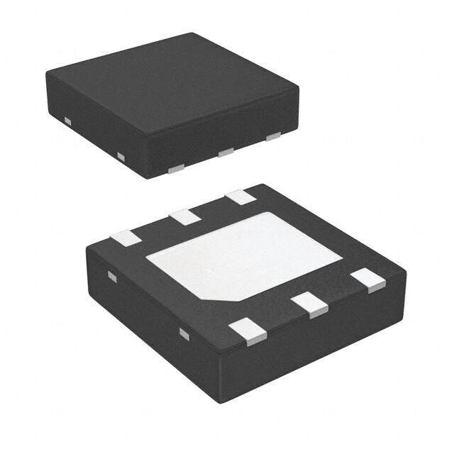
Device Information(1)
PART NUMBER
LM2734Z
PACKAGE
BODY SIZE (NOM)
WSON (6)
3.00 mm × 3.00 mm
SOT (6)
1.60 mm × 2.90 mm
(1) For all available packages, see the orderable addendum at
the end of the data sheet.
Typical Application Circuit
Efficiency vs Load Current
D2
VIN
BOOST
VIN
C3
C1
L1
SW
VOUT
LM2734
ON
D1
EN
C2
R1
OFF
FB
GND
R2
1
An IMPORTANT NOTICE at the end of this data sheet addresses availability, warranty, changes, use in safety-critical applications,
intellectual property matters and other important disclaimers. PRODUCTION DATA.
�LM2734Z, LM2734Z-Q1
SNVS334F – JANUARY 2005 – REVISED JANUARY 2016
www.ti.com
Table of Contents
1
2
3
4
5
6
7
Features ..................................................................
Applications ...........................................................
Description .............................................................
Revision History.....................................................
Pin Configuration and Functions .........................
Specifications.........................................................
1
1
1
2
3
4
6.1
6.2
6.3
6.4
6.5
6.6
4
4
4
5
5
6
Absolute Maximum Ratings ......................................
ESD Ratings..............................................................
Recommended Operating Conditions.......................
Thermal Information ..................................................
Electrical Characteristics...........................................
Typical Characteristics ..............................................
Detailed Description .............................................. 7
7.1 Overview ................................................................... 7
7.2 Functional Block Diagram ......................................... 7
7.3 Feature Description................................................... 7
7.4 Device Functional Modes........................................ 11
8
Application and Implementation ........................ 12
8.1 Application Information............................................ 12
8.2 Typical Applications ................................................ 12
9 Power Supply Recommendations...................... 26
10 Layout................................................................... 26
10.1 Layout Guidelines ................................................. 26
10.2 Layout Examples................................................... 27
11 Device and Documentation Support ................. 28
11.1
11.2
11.3
11.4
11.5
11.6
Device Support......................................................
Documentation Support ........................................
Community Resources..........................................
Trademarks ...........................................................
Electrostatic Discharge Caution ............................
Glossary ................................................................
28
28
28
28
28
28
12 Mechanical, Packaging, and Orderable
Information ........................................................... 28
4 Revision History
NOTE: Page numbers for previous revisions may differ from page numbers in the current version.
Changes from Revision E (April 2013) to Revision F
Page
•
Added ESD Ratings table, Feature Description section, Device Functional Modes section, Application and
Implementation section, Power Supply Recommendations section, Layout section, Device and Documentation
Support section, and Mechanical, Packaging, and Orderable Information section................................................................ 1
•
Removed soldering information ............................................................................................................................................. 4
Changes from Revision D (April 2013) to Revision E
•
2
Page
Changed layout of National Data Sheet to TI format ........................................................................................................... 25
Submit Documentation Feedback
Copyright © 2005–2016, Texas Instruments Incorporated
Product Folder Links: LM2734Z LM2734Z-Q1
�LM2734Z, LM2734Z-Q1
www.ti.com
SNVS334F – JANUARY 2005 – REVISED JANUARY 2016
5 Pin Configuration and Functions
DDC Package
6-Pin SOT
Top View
BOOST
1
6
SW
GND
2
5
VIN
FB
3
4
EN
NGG Package
6-Pin WSON
Top View
FB
1
GND
2
BOOST
3
DAP
6
EN
5
VIN
4
SW
Pin Functions
PIN
TYPE (1)
DESCRIPTION
NAME
SOT
WSON
BOOST
1
3
I
Boost voltage that drives the internal NMOS control switch. A bootstrap
capacitor is connected between the BOOST and SW pins.
DAP
—
—
P
The die attach pad is internally connected to GND.
EN
4
6
I
Enable control input. Logic high enables operation. Do not allow this pin to float
or be greater than VIN + 0.3 V.
FB
3
1
I
Feedback pin. Connect FB to the external resistor divider to set output voltage.
GND
2
2
P
Signal and Power ground pin. Place the bottom resistor of the feedback network
as close as possible to this pin for accurate regulation.
SW
6
4
O
Output switch. Connects to the inductor, catch diode, and bootstrap capacitor.
VIN
5
5
P
Input supply voltage. Connect a bypass capacitor to this pin.
(1)
I –Input, O – Output, P – Power
Copyright © 2005–2016, Texas Instruments Incorporated
Product Folder Links: LM2734Z LM2734Z-Q1
Submit Documentation Feedback
3
�LM2734Z, LM2734Z-Q1
SNVS334F – JANUARY 2005 – REVISED JANUARY 2016
www.ti.com
6 Specifications
6.1 Absolute Maximum Ratings
See
(1) (2)
VIN
MIN
MAX
UNIT
Input voltage
–0.5
24
V
SW voltage
–0.5
24
V
Boost voltage
–0.5
30
V
Boost to SW voltage
–0.5
6
V
FB voltage
–0.5
3
V
EN voltage
–0.5
VIN + 0.3
V
150
°C
150
°C
TJ
Junction temperature
Tstg
Storage temperature
(1)
(2)
–65
Stresses beyond those listed under Absolute Maximum Ratings may cause permanent damage to the device. These are stress ratings
only, which do not imply functional operation of the device at these or any other conditions beyond those indicated under Recommended
Operating Conditions. Exposure to absolute-maximum-rated conditions for extended periods may affect device reliability.
If Military/Aerospace specified devices are required, please contact the Texas Instruments Sales Office/ Distributors for availability and
specifications.
6.2 ESD Ratings
VALUE
V(ESD)
(1)
(2)
Electrostatic
discharge
Human-body model (HBM), per AEC Q100-002 (1) (2)
±2000
Charged-device model (CDM), per AEC Q100-002
±1000
UNIT
V
AEC Q100-002 indicates that HBM stressing shall be in accordance with the ANSI/ESDA/JEDEC JS-001 specification.
Human-body model, 1.5 kΩ in series with 100 pF.
6.3 Recommended Operating Conditions
VIN
TJ
4
MIN
MAX
3
20
V
SW voltage
–0.5
20
V
Boost voltage
V
Input voltage
UNIT
–0.5
25
Boost to SW voltage
1.6
5.5
V
Junction temperature
–40
125
°C
Submit Documentation Feedback
Copyright © 2005–2016, Texas Instruments Incorporated
Product Folder Links: LM2734Z LM2734Z-Q1
�LM2734Z, LM2734Z-Q1
www.ti.com
SNVS334F – JANUARY 2005 – REVISED JANUARY 2016
6.4 Thermal Information
LM2734Z
THERMAL METRIC (1)
DDC (SOT)
NGG (WSON)
6 PINS
6 PINS
UNIT
RθJA
Junction-to-ambient thermal resistance (2)
180.3
56.2
°C/W
RθJC(top)
Junction-to-case (top) thermal resistance
51.6
52.6
°C/W
RθJB
Junction-to-board thermal resistance
27.7
30.7
°C/W
ψJT
Junction-to-top characterization parameter
1.2
0.9
°C/W
ψJB
Junction-to-board characterization parameter
27.3
30.8
°C/W
RθJC(bot)
Junction-to-case (bottom) thermal resistance
—
10.7
°C/W
(1)
(2)
For more information about traditional and new thermal metrics, see the Semiconductor and IC Package Thermal Metrics application
report (SPRA953).
Thermal shutdown occurs if the junction temperature exceeds 165°C. The maximum power dissipation is a function of TJ(MAX), RθJA and
TA . The maximum allowable power dissipation at any ambient temperature is PD = (TJ(MAX) – TA)/RθJA . All numbers apply for packages
soldered directly onto a 3-in × 3-in printed-circuit-board with 2-oz. copper on 4 layers in still air. For a 2-layer board using 1-oz. copper in
still air, RθJA = 204°C/W.
6.5 Electrical Characteristics
All typical specifications are for TJ = 25°C, and all maximum and minimum limits apply over the full operating temperature
range (TJ = –40°C to 125°C). VIN = 5 V, VBOOST – VSW = 5 V (unless otherwise noted). Data sheet minimum and maximum
specification limits are specified by design, test, or statistical analysis.
PARAMETER
TEST CONDITIONS
VFB
Feedback voltage
ΔVFB/ΔVIN
Feedback voltage line regulation
VIN = 3 V to 20 V
IFB
Feedback input bias current
Sink and source
Undervoltage lockout
VIN Rising
Undervoltage lockout
VIN Falling
UVLO
UVLO hysteresis
MIN (1)
TYP (2)
MAX (1)
0.784
0.8
0.816
0.01
V
%/V
10
250
2.74
2.90
nA
2
2.3
0.30
0.44
0.62
3.6
MHz
FSW
Switching frequency
2.2
3.0
DMAX
Maximum duty cycle
78%
85%
DMIN
Minimum duty Cycle
RDS(ON)
Switch ON resistance
ICL
UNIT
V
8%
VBOOST - VSW = 3 V
(SOT Package)
300
600
mΩ
VBOOST - VSW = 3 V
(WSON Package)
340
650
mΩ
Switch current limit
VBOOST - VSW = 3 V
1.7
2.5
A
Quiescent current
Switching
1.5
2.5
mA
Quiescent current (shutdown)
VEN = 0 V
30
Boost pin current
(Switching)
Shutdown threshold voltage
VEN Falling
Enable threshold voltage
VEN Rising
IEN
Enable pin current
Sink/source
ISW
Switch leakage
IQ
IBOOST
VEN_TH
(1)
(2)
1.2
4.25
nA
6
0.4
1.8
mA
V
10
nA
40
nA
Specified to Texas Instruments' Average Outgoing Quality Level (AOQL).
Typicals represent the most likely parametric norm.
Copyright © 2005–2016, Texas Instruments Incorporated
Product Folder Links: LM2734Z LM2734Z-Q1
Submit Documentation Feedback
5
�LM2734Z, LM2734Z-Q1
SNVS334F – JANUARY 2005 – REVISED JANUARY 2016
www.ti.com
6.6 Typical Characteristics
at VIN = 5 V, VBOOST - VSW = 5 V, L1 = 2.2 µH and TA = 25°C (unless otherwise noted)
VOUT = 5 V
VOUT = 3.3 V
Figure 1. Efficiency vs Load Current
Figure 2. Efficiency vs Load Current
VOUT = 1.5 V
Figure 3. Efficiency vs Load Current
VOUT = 1.5 V
IOUT = 500 mA
Figure 4. Oscillator Frequency vs Temperature
VOUT = 3.3 V
Figure 5. Line Regulation
6
Submit Documentation Feedback
IOUT = 500 mA
Figure 6. Line Regulation
Copyright © 2005–2016, Texas Instruments Incorporated
Product Folder Links: LM2734Z LM2734Z-Q1
�LM2734Z, LM2734Z-Q1
www.ti.com
SNVS334F – JANUARY 2005 – REVISED JANUARY 2016
7 Detailed Description
7.1 Overview
The LM2734Z is a constant frequency buck regulator that can deliver load current of 1 A. Device is optimized for
high-efficiency operation and includes a number of features that make it suitable for demanding applications.
High switching frequency allows for use of small external components enabling small solution size and saving
board space.
Device is designed to operate from wide input voltage range up to 20 V, making it ideal for wide range of
applications (such as automotive, industrial, communications, and so forth). LM2734Z can be controlled through
shutdown pin, consuming only 30 nA in standby mode, making it very appealing for applications that demand
very low standby power consumption.
7.2 Functional Block Diagram
VIN
VIN
Current-Sense Amplifier
OFF
EN
Internal
Regulator
and
Enable
Circuit
+
-
BOOST
VBOOST
Under
Voltage
Lockout
Oscillator
CIN
D2
Thermal
Shutdown
Current
Limit
Output
Control
Logic
Reset
Pulse
+
ISENSE
+
+
Corrective Ramp
0.3:
Switch
Driver
SW
OVP
Comparator
-
ON
RSENSE
Error
Signal
D
1
+
PWM
Comparator
CBOOST
VSW L
IL
VOUT
COUT
0.88V
+
-
R
1
FB
Internal
Compensation
+
Error Amplifier
+
-
VREF
0.8V
R
2
GND
7.3 Feature Description
7.3.1 Theory of Operation
The LM2734Z is a constant frequency PWM buck regulator IC that delivers a 1-A load current. The regulator has
a preset switching frequency of 3 MHz. This high frequency allows the LM2734Z to operate with small surface
mount capacitors and inductors, resulting in a DC–DC converter that requires a minimum amount of board
space. The LM2734Z is internally compensated, so it is simple to use, and requires few external components.
The LM2734Z uses current-mode control to regulate the output voltage.
The following operating description of the LM2734Z refers to the Functional Block Diagram and to the waveforms
in Figure 7. The LM2734Z supplies a regulated output voltage by switching the internal NMOS control switch at
constant frequency and variable duty cycle. A switching cycle begins at the falling edge of the reset pulse
generated by the internal oscillator. When this pulse goes low, the output control logic turns on the internal
NMOS control switch. During this ON-time, the SW pin voltage (VSW) swings up to approximately VIN, and the
inductor current (IL) increases with a linear slope. IL is measured by the current-sense amplifier, which generates
an output proportional to the switch current. The sense signal is summed with the corrective ramp of the
Copyright © 2005–2016, Texas Instruments Incorporated
Product Folder Links: LM2734Z LM2734Z-Q1
Submit Documentation Feedback
7
�LM2734Z, LM2734Z-Q1
SNVS334F – JANUARY 2005 – REVISED JANUARY 2016
www.ti.com
Feature Description (continued)
regulator and compared to the output of the error amplifier, which is proportional to the difference between the
feedback voltage and VREF. When the PWM comparator output goes high, the output switch turns off until the
next switching cycle begins. During the switch OFF-time, inductor current discharges through Schottky diode D1,
which forces the SW pin to swing below ground by the forward voltage (VD) of the catch diode. The regulator
loop adjusts the duty cycle (D) to maintain a constant output voltage.
VSW
D = TON/TSW
VIN
SW
Voltage
TOFF
TON
0
VD
IL
t
TSW
IPK
Inductor
Current
t
0
Figure 7. LM2734Z Waveforms of SW Pin Voltage and Inductor Current
7.3.2 Boost Function
Capacitor CBOOST and diode D2 in Figure 8 are used to generate a voltage VBOOST. VBOOST - VSW is the gate drive
voltage to the internal NMOS control switch. To properly drive the internal NMOS switch during its ON-time,
VBOOST needs to be at least 1.6 V greater than VSW. Although the LM2734Z operates with this minimum voltage,
it may not have sufficient gate drive to supply large values of output current. Therefore, TI recommends that
VBOOST be greater than 2.5 V above VSW for best efficiency. VBOOST – VSW must not exceed the maximum
operating limit of 5.5 V.
5.5 V > VBOOST – VSW > 2.5 V for best performance.
VBOOST
D2
BOOST
VIN
VIN
CIN
LM2734
CBOOST
L
SW
VOUT
GND
COUT
D1
Figure 8. VOUT Charges CBOOST
When the LM2734Z starts up, internal circuitry from the BOOST pin supplies a maximum of 20 mA to CBOOST.
This current charges CBOOST to a voltage sufficient to turn the switch on. The BOOST pin continues to source
current to CBOOST until the voltage at the feedback pin is greater than 0.76 V.
8
Submit Documentation Feedback
Copyright © 2005–2016, Texas Instruments Incorporated
Product Folder Links: LM2734Z LM2734Z-Q1
�LM2734Z, LM2734Z-Q1
www.ti.com
SNVS334F – JANUARY 2005 – REVISED JANUARY 2016
Feature Description (continued)
There are various methods to derive VBOOST:
1. From the input voltage (VIN)
2. From the output voltage (VOUT)
3. From an external distributed voltage rail (VEXT)
4. From a shunt or series zener diode
In Functional Block Diagram, capacitor CBOOST and diode D2 supply the gate-drive current for the NMOS switch.
Capacitor CBOOST is charged through diode D2 by VIN. During a normal switching cycle, when the internal NMOS
control switch is off (TOFF) (refer to Figure 7), VBOOST equals VIN minus the forward voltage of D2 (VFD2), during
which the current in the inductor (L) forward biases the Schottky diode D1 (VFD1). Therefore the voltage stored
across CBOOST is calculated using Equation 1.
VBOOST –VSW = VIN – VFD2 + VFD1
(1)
When the NMOS switch turns on (TON), the switch pin rises to:
VSW = VIN – (RDSON x IL),
(2)
forcing VBOOST to rise thus reverse biasing D2. The voltage at VBOOST is then:
VBOOST = 2 VIN – (RDSON x IL) – VFD2 + VFD1
(3)
which is approximately:
2 VIN – 0.4 V
(4)
for many applications. Thus the gate-drive voltage of the NMOS switch is approximately:
VIN –0.2 V
(5)
An alternate method for charging CBOOST is to connect D2 to the output as shown in Figure 8. The output voltage
must be between 2.5 V and 5.5 V, so that proper gate voltage is applied to the internal switch. In this circuit,
CBOOST provides a gate drive voltage that is slightly less than VOUT.
In applications where both VIN and VOUT are greater than 5.5 V, or less than 3 V, CBOOST cannot be charged
directly from these voltages. If VIN and VOUT are greater than 5.5 V, CBOOST can be charged from VIN or VOUT
minus a Zener voltage by placing a Zener diode D3 in series with D2, as shown in Figure 9. When using a series
Zener diode from the input, ensure that the regulation of the input supply does not create a voltage that falls
outside the recommended VBOOST voltage.
(VINMAX – VD3) < 5.5V
(VINMIN – VD3) > 1.6V
(6)
(7)
D2
D3
VIN
VIN
CIN
BOOST
VBOOST
CBOOST
LM2734
L
VOUT
SW
GND
D1
C OUT
Figure 9. Zener Reduces Boost Voltage from VIN
An alternative method is to place the Zener diode D3 in a shunt configuration as shown in Figure 10. A small
350-mW to 500-mW, 5.1-V Zener in a SOT or SOD package can be used for this purpose. A small ceramic
capacitor such as a 6.3-V, 0.1-µF capacitor (C4) must be placed in parallel with the Zener diode. When the
internal NMOS switch turns on, a pulse of current is drawn to charge the internal NMOS gate capacitance. The
0.1-µF parallel shunt capacitor ensures that the VBOOST voltage is maintained during this time.
Copyright © 2005–2016, Texas Instruments Incorporated
Product Folder Links: LM2734Z LM2734Z-Q1
Submit Documentation Feedback
9
�LM2734Z, LM2734Z-Q1
SNVS334F – JANUARY 2005 – REVISED JANUARY 2016
www.ti.com
Feature Description (continued)
Resistor R3 must be chosen to provide enough RMS current to the Zener diode (D3) and to the BOOST pin. A
recommended choice for the Zener current (IZENER) is 1 mA. The current IBOOST into the BOOST pin supplies the
gate current of the NMOS control switch and varies typically according to Equation 8.
IBOOST = (D + 0.5) × (VZENER – VD2) mA
where
•
•
•
•
•
D is the duty cycle
VZENER and VD2 are in volts
IBOOST is in milliamps
VZENER is the voltage applied to the anode of the boost diode (D2)
VD2 is the average forward voltage across D2
(8)
NOTE
Equation 8 for IBOOST gives typical current.
For the worst case IBOOST, increase the current by 25%. In that case, the worse-case boost current is:
IBOOST-MAX = 1.25 × IBOOST
(9)
R3 is then given by Equation 10.
R3 = (VIN - VZENER) / (1.25 × IBOOST + IZENER)
(10)
For example, let VIN = 10 V, VZENER = 5 V, VD2 = 0.7 V, IZENER = 1 mA, and duty cycle D = 50%. Then:
IBOOST = (0.5 + 0.5) × (5 - 0.7) mA = 4.3 mA
R3 = (10 V - 5 V) / (1.25 × 4.3 mA + 1 mA) = 787 Ω
(11)
(12)
VZ
C4
D2
D3
R3
VIN
VIN
BOOST
CBOOST
LM2734
C IN
VBOOST
L
SW
VOUT
GND
COUT
D1
Figure 10. Boost Voltage Supplied from the Shunt Zener on VIN
7.3.3 Soft-Start
This function forces VOUT to increase at a controlled rate during start-up. During soft-start, the reference voltage
of the error amplifier ramps from 0 V to its nominal value of 0.8 V in approximately 200 µs. This forces the
regulator output to ramp up in a more linear and controlled fashion, which helps reduce inrush current.
7.3.4 Output Overvoltage Protection
The overvoltage comparator compares the FB pin voltage to a voltage that is 10% higher than the internal
reference Vref. Once the FB pin voltage goes 10% above the internal reference, the internal NMOS control
switch is turned off, which allows the output voltage to decrease toward regulation.
10
Submit Documentation Feedback
Copyright © 2005–2016, Texas Instruments Incorporated
Product Folder Links: LM2734Z LM2734Z-Q1
�LM2734Z, LM2734Z-Q1
www.ti.com
SNVS334F – JANUARY 2005 – REVISED JANUARY 2016
Feature Description (continued)
7.3.5 Undervoltage Lockout
Undervoltage lockout (UVLO) prevents the LM2734Z from operating until the input voltage exceeds 2.74 V
(typical).
The UVLO threshold has approximately 440 mV of hysteresis, so the part operates until VIN drops below 2.3 V
(typical). Hysteresis prevents the part from turning off during power up if VIN is non-monotonic.
7.3.6 Current Limit
The LM2734Z uses cycle-by-cycle current limiting to protect the output switch. During each switching cycle, a
current limit comparator detects if the output switch current exceeds 1.7 A (typical), and turns off the switch until
the next switching cycle begins.
7.4 Device Functional Modes
7.4.1 Enable Pin and Shutdown Mode
The LM2734Z has a shutdown mode that is controlled by the enable pin (EN). When a logic low voltage is
applied to EN, the part is in shutdown mode and its quiescent current drops to typically 30 nA. Switch leakage
adds another 40 nA from the input supply. The voltage at this pin must never exceed VIN + 0.3 V.
7.4.2 Thermal Shutdown
Thermal shutdown limits total power dissipation by turning off the output switch when the IC junction temperature
exceeds 165°C. After thermal shutdown occurs, the output switch doesn’t turn on until the junction temperature
drops to approximately 150°C.
Copyright © 2005–2016, Texas Instruments Incorporated
Product Folder Links: LM2734Z LM2734Z-Q1
Submit Documentation Feedback
11
�LM2734Z, LM2734Z-Q1
SNVS334F – JANUARY 2005 – REVISED JANUARY 2016
www.ti.com
8 Application and Implementation
NOTE
Information in the following applications sections is not part of the TI component
specification, and TI does not warrant its accuracy or completeness. TI’s customers are
responsible for determining suitability of components for their purposes. Customers should
validate and test their design implementation to confirm system functionality.
8.1 Application Information
This device operates with wide input voltage in the range of 3 V to 20 V and provides regulated output voltage in
the range of 0.8 V to 18 V. This device is optimized for high-efficiency operation with a minimum number of
external components, making it ideal for applications where board space is constrained.
8.2 Typical Applications
8.2.1 LM2734Z Design Example 1
D2
VIN
BOOST
VIN
C3
C1
L1
R3
VOUT
SW
LM2734
ON
D1
EN
C2
R1
OFF
FB
GND
R2
Figure 11. VBOOST Derived from VIN
Operating Conditions: 5 V to 1.5 V / 1 A
8.2.1.1 Design Requirements
Table 1 lists the operating conditions for the design example 1.
Table 1. Design Parameters
PARAMETER
VALUE
PARAMETER
VALUE
VIN
5.0 V
POUT
2.5 W
VOUT
2.5 V
PDIODE
151 mW
IOUT
1.0 A
PIND
75 mW
VD
0.35 V
PSWF
53 mW
Freq
3 MHz
PSWR
53 mW
IQ
1.5 mA
PCOND
187 mW
TRISE
8 ns
PQ
7.5 mW
TFALL
8 ns
PBOOST
21 mW
RDSON
330 mΩ
PLOSS
548 mW
INDDCR
75 mΩ
D
56.8%
12
Submit Documentation Feedback
Copyright © 2005–2016, Texas Instruments Incorporated
Product Folder Links: LM2734Z LM2734Z-Q1
�LM2734Z, LM2734Z-Q1
www.ti.com
SNVS334F – JANUARY 2005 – REVISED JANUARY 2016
8.2.1.2 Detailed Design Procedure
8.2.1.2.1 Inductor Selection
The Duty Cycle (D) can be approximated quickly using the ratio of output voltage (VO) to input voltage (VIN) as
shown in Equation 13.
VO
D=
VIN
(13)
The catch diode (D1) forward voltage drop and the voltage drop across the internal NMOS must be included to
calculate a more accurate duty cycle. Calculate D with Equation 14.
VO + VD
D=
VIN + VD - VSW
(14)
VSW can be approximated by Equation 15.
VSW = IO x RDS(ON)
(15)
The diode forward drop (VD) can range from 0.3 V to 0.7 V depending on the quality of the diode. The lower VD
is, the higher the operating efficiency of the converter.
The inductor value determines the output ripple current. Lower inductor values decrease the size of the inductor,
but increase the output ripple current. An increase in the inductor value decreases the output ripple current. The
ratio of ripple current (ΔiL) to output current (IO) is optimized when it is set between 0.3 and 0.4 at 1 A. The ratio r
is defined in Equation 16.
r=
'iL
lO
(16)
One must also ensure that the minimum current limit (1.2 A) is not exceeded, so the peak current in the inductor
must be calculated. The peak current (ILPK) in the inductor is calculated by Equation 17.
ILPK = IO + ΔIL/2
(17)
If r = 0.5 at an output of 1 A, the peak current in the inductor is 1.25 A. The minimum specified current limit over
all operating conditions is 1.2 A. One can either reduce r to 0.4 resulting in a 1.2-A peak current, or make the
engineering judgement that 50 mA over is safe enough with a 1.7-A typical current limit and 6 sigma limits. When
the designed maximum output current is reduced, the ratio r can be increased. At a current of 0.1 A, r can be
made as high as 0.9. The ripple ratio can be increased at lighter loads because the net ripple is actually quite
low, and if r remains constant the inductor value can be made quite large. An equation empirically developed for
the maximum ripple ratio at any current below 2 A is:
r = 0.387 × IOUT-0.3667
(18)
NOTE
Use this as a guideline.
The LM2734Z operates at frequencies allowing the use of ceramic output capacitors without compromising
transient response. Ceramic capacitors allow higher inductor ripple without significantly increasing output ripple.
See the Output Capacitor section for more details on calculating output voltage ripple.
Copyright © 2005–2016, Texas Instruments Incorporated
Product Folder Links: LM2734Z LM2734Z-Q1
Submit Documentation Feedback
13
�LM2734Z, LM2734Z-Q1
SNVS334F – JANUARY 2005 – REVISED JANUARY 2016
www.ti.com
Now that the ripple current or ripple ratio is determined, the inductance is calculated by Equation 19.
L=
VO + VD
IO x r x fS
x (1-D)
where
•
•
fs is the switching frequency
IO is the output current
(19)
When selecting an inductor, make sure that it is capable of supporting the peak output current without saturating.
Inductor saturation results in a sudden reduction in inductance and prevent the regulator from operating correctly.
Because of the speed of the internal current limit, the peak current of the inductor need only be specified for the
required maximum output current. For example, if the designed maximum output current is 0.5 A and the peak
current is 0.7 A, then the inductor must be specified with a saturation current limit of >0.7 A. There is no need to
specify the saturation or peak current of the inductor at the 1.7-A typical switch current limit. The difference in
inductor size is a factor of 5. Because of the operating frequency of the LM2734Z, ferrite based inductors are
preferred to minimize core losses. This presents little restriction because the variety of ferrite based inductors is
huge. Lastly, inductors with lower series resistance (DCR) provides better operating efficiency. For
recommended inductors, see the design examples in Typical Applications.
8.2.1.2.2 Input Capacitor
An input capacitor is necessary to ensure that VIN does not drop excessively during switching transients. The
primary specifications of the input capacitor are capacitance, voltage, RMS current rating, and ESL (Equivalent
Series Inductance). The recommended input capacitance is 10 µF, although 4.7 µF works well for input voltages
below 6 V. The input voltage rating is specifically stated by the capacitor manufacturer. Make sure to check any
recommended deratings and also verify if there is any significant change in capacitance at the operating input
voltage and the operating temperature. The input capacitor maximum RMS input current rating (IRMS-IN) must be
greater than:
IRMS-IN = IO x
r2
D x 1-D +
12
(20)
As seen in Equation 20, the maximum RMS capacitor current occurs when D = 0.5. Always calculate the RMS at
the point where the duty cycle, D, is closest to 0.5. The ESL of an input capacitor is usually determined by the
effective cross sectional area of the current path. A large leaded capacitor has high ESL and a 0805 ceramic
chip capacitor has very low ESL. At the operating frequencies of the LM2734Z, certain capacitors may have an
ESL so large that the resulting impedance (2πfL) is higher than that required to provide stable operation. As a
result, surface mount capacitors are strongly recommended. Sanyo POSCAP, Tantalum or Niobium, Panasonic
SP or Cornell Dubilier ESR, and multilayer ceramic capacitors (MLCC) are all good choices for both input and
output capacitors and have very low ESL. For MLCCs, TI recommends using X7R or X5R dielectrics. Consult
capacitor manufacturer data sheet to see how rated capacitance varies over operating conditions.
8.2.1.2.3 Output Capacitor
The output capacitor is selected based upon the desired output ripple and transient response. The initial current
of a load transient is provided mainly by the output capacitor. The output ripple of the converter is shown in
Equation 21.
'VO = 'iL x (RESR +
1
)
8 x fS x CO
(21)
When using MLCCs, the ESR is typically so low that the capacitive ripple may dominate. When this occurs, the
output ripple is approximately sinusoidal and 90° phase shifted from the switching action. Given the availability
and quality of MLCCs and the expected output voltage of designs using the LM2734Z, there is really no need to
review any other capacitor technologies. Another benefit of ceramic capacitors is their ability to bypass high
frequency noise. A certain amount of switching edge noise couples through parasitic capacitances in the inductor
14
Submit Documentation Feedback
Copyright © 2005–2016, Texas Instruments Incorporated
Product Folder Links: LM2734Z LM2734Z-Q1
�LM2734Z, LM2734Z-Q1
www.ti.com
SNVS334F – JANUARY 2005 – REVISED JANUARY 2016
to the output. A ceramic capacitor bypasses this noise while a tantalum will not. Because the output capacitor is
one of the two external components that control the stability of the regulator control loop, most applications will
require a minimum at 10 µF of output capacitance. Capacitance can be increased significantly with little detriment
to the regulator stability. Like the input capacitor, recommended multilayer ceramic capacitors are X7R or X5R.
Again, verify actual capacitance at the desired operating voltage and temperature.
Check the RMS current rating of the capacitor. The RMS current rating of the capacitor chosen must also meet
Equation 22.
r
12
IRMS-OUT = IO x
(22)
8.2.1.2.4 Catch Diode
The catch diode (D1) conducts during the switch OFF-time. A Schottky diode is recommended for its fast
switching times and low forward voltage drop. The catch diode must be chosen so that its current rating is
greater than Equation 23.
ID1 = IO x (1-D)
(23)
The reverse breakdown rating of the diode must be at least the maximum input voltage plus appropriate margin.
To improve efficiency choose a Schottky diode with a low forward voltage drop.
8.2.1.2.5 Boost Diode
A standard diode such as the 1N4148 type is recommended. For VBOOST circuits derived from voltages less than
3.3 V, a small-signal Schottky diode is recommended for greater efficiency. A good choice is the BAT54 small
signal diode.
8.2.1.2.6 Boost Capacitor
A ceramic 0.01-µF capacitor with a voltage rating of at least 6.3 V is sufficient. The X7R and X5R MLCCs
provide the best performance.
8.2.1.2.7 Output Voltage
The output voltage is set using Equation 24 where R2 is connected between the FB pin and GND, and R1 is
connected between VO and the FB pin. A good value for R2 is 10 kΩ.
R1 =
VO
VREF
- 1 x R2
(24)
8.2.1.2.8 Calculating Efficiency, and Junction Temperature
The complete LM2734Z DC–DC converter efficiency can be calculated in the following manner:
POUT
K=
PIN
(25)
Or
POUT
K=
POUT + PLOSS
(26)
Calculations for determining the most significant power losses are shown below. Other losses totaling less than
2% are not discussed.
Power loss (PLOSS) is the sum of two basic types of losses in the converter, switching and conduction.
Conduction losses usually dominate at higher output loads, where as switching losses remain relatively fixed and
dominate at lower output loads. The first step in determining the losses is to calculate the duty cycle (D).
VOUT + VD
D=
VIN + VD - VSW
(27)
Copyright © 2005–2016, Texas Instruments Incorporated
Product Folder Links: LM2734Z LM2734Z-Q1
Submit Documentation Feedback
15
�LM2734Z, LM2734Z-Q1
SNVS334F – JANUARY 2005 – REVISED JANUARY 2016
www.ti.com
VSW is the voltage drop across the internal NFET when it is on, and is equal to Equation 28.
VSW = IOUT × RDSON
(28)
VD is the forward voltage drop across the Schottky diode. It can be obtained from the Electrical Characteristics
section. If the voltage drop across the inductor (VDCR) is accounted for, use Equation 29 to calculate the duty
cycle.
VO + VD + VDCR
D=
VIN + VD - VSW
(29)
This usually gives only a minor duty cycle change, and has been omitted in the examples for simplicity.
The conduction losses in the free-wheeling Schottky diode are calculated using Equation 30.
PDIODE = VD × IOUT(1-D)
(30)
Often this is the single most significant power loss in the circuit. Take care choosing a Schottky diode that has a
low forward voltage drop.
Another significant external power loss is the conduction loss in the output inductor. The equation can be
simplified to Equation 31.
PIND = IOUT2 × RDCR
(31)
The LM2734Z conduction loss is mainly associated with the internal NFET, as shown in Equation 32.
PCOND = IOUT2 ×RDSON x D
(32)
Switching losses are also associated with the internal NFET. They occur during the switch on and off transition
periods, where voltages and currents overlap resulting in power loss. The simplest means to determine this loss
is to empirically measure the rise and fall times (10% to 90%) of the switch at the switch node using Equation 33
through Equation 35.
PSWF = 1/2 (VIN × IOUT × freq × TFALL)
PSWR = 1/2(VIN x IOUT x freq x TRISE)
PSW = PSWF + PSWR
(33)
(34)
(35)
Table 2. Typical Rise and Fall Times vs Input Voltage
VIN
TRISE
TFALL
5V
8 ns
4 ns
10 V
9 ns
6 ns
15 V
10 ns
7 ns
Another loss is the power required for operation of the internal circuitry:
PQ = IQ x VIN
(36)
IQ is the quiescent operating current, and is typically around 1.5 mA. The other operating power that needs to be
calculated is that required to drive the internal NFET:
PBOOST = IBOOST x VBOOST
(37)
VBOOST is normally between 3 VDC and 5 VDC. The IBOOST rms current is approximately 4.25 mA. Total power
losses are:
6PCOND + PSW + PDIODE + PIND + PQ + PBOOST = PLOSS
(38)
8.2.1.2.9 Calculating the LM2734Z Junction Temperature
Thermal Definitions:
TJ = Chip junction temperature
TA = Ambient temperature
RθJC = Thermal resistance from chip junction to device case
RθJA = Thermal resistance from chip junction to ambient air
16
Submit Documentation Feedback
Copyright © 2005–2016, Texas Instruments Incorporated
Product Folder Links: LM2734Z LM2734Z-Q1
�LM2734Z, LM2734Z-Q1
www.ti.com
SNVS334F – JANUARY 2005 – REVISED JANUARY 2016
Figure 12. Cross-Sectional View of Integrated Circuit Mounted on a Printed Circuit Board
Heat in the LM2734Z due to internal power dissipation is removed through conduction and/or convection.
Conduction: Heat transfer occurs through cross sectional areas of material. Depending on the material, the
transfer of heat can be considered to have poor to good thermal conductivity properties (insulator vs conductor).
Heat Transfer goes as:
silicon→package→lead frame→PCB.
Convection: Heat transfer is by means of airflow. This could be from a fan or natural convection. Natural
convection occurs when air currents rise from the hot device to cooler air.
Thermal impedance is defined as shown in Equation 39.
RT =
'T
Power
(39)
Thermal impedance from the silicon junction to the ambient air is defined as shown in Equation 40.
TJ - TA
RTJA =
Power
(40)
This impedance can vary depending on the thermal properties of the PCB. This includes PCB size, weight of
copper used to route traces and ground plane, and number of layers within the PCB. The type and number of
thermal vias can also make a large difference in the thermal impedance. Thermal vias are necessary in most
applications. They conduct heat from the surface of the PCB to the ground plane. Four to six thermal vias must
be placed under the exposed pad to the ground plane if the WSON package is used. If the 6-pin SOT package is
used, place two to four thermal vias close to the ground pin of the device.
The data sheet specifies two different RθJA numbers for the thin SOT–6 package. The two numbers show the
difference in thermal impedance for a four-layer board with 2-oz. copper traces, versus a four-layer board with 1oz. copper. RθJA equals 120°C/W for 2-oz. copper traces and GND plane, and 235°C/W for 1-oz. copper traces
and GND plane.
The first method to accurately measure the silicon temperature for a given application, two methods can be used.
The first method requires the user to know the thermal impedance of the silicon junction to case. (RθJC) is
approximately 80°C/W for the thin SOT-6 package. Knowing the internal dissipation from the efficiency
calculation given previously, and the case temperature, which can be empirically measured on the bench:
TJ - TC
RTJA =
Power
(41)
Therefore:
TJ = (RθJC × PLOSS) + TC
(42)
Copyright © 2005–2016, Texas Instruments Incorporated
Product Folder Links: LM2734Z LM2734Z-Q1
Submit Documentation Feedback
17
�LM2734Z, LM2734Z-Q1
SNVS334F – JANUARY 2005 – REVISED JANUARY 2016
www.ti.com
6PCOND + PSWF + PSWR + PQ + PBOOST = PINTERNAL
PINTERNAL = 322 mW
TJ = (RTJC x Power) + TC = 80oC/W x 322 mW + TC
(43)
The second method can give a very accurate silicon junction temperature. The first step is to determine RθJA of
the application. The LM2734Z has overtemperature protection circuitry. When the silicon temperature reaches
165°C, the device stops switching. The protection circuitry has a hysteresis of 15°C. Once the silicon
temperature has decreased to approximately 150°C, the device starts to switch again. Knowing this, the RθJA for
any PCB can be characterized during the early stages of the design by raising the ambient temperature in the
given application until the circuit enters thermal shutdown. If the SW-pin is monitored, it is obvious when the
internal NFET stops switching indicating a junction temperature of 165°C. Knowing the internal power dissipation
from the above methods, the junction temperature and the ambient temperature, RθJA can be determined using
Equation 44.
165oC - TA
RTJA =
PINTERNAL
(44)
Once this is determined, the maximum ambient temperature allowed for a desired junction temperature can be
found using Equation 45.
6PCOND + PSWF + PSWR + PQ + PBOOST = PINTERNAL
PINTERNAL = 322 mW
(45)
Using a standard Texas Instruments 6-pin SOT demonstration board to determine the RθJA of the board. The four
layer PCB is constructed using FR4 with 1/2-oz copper traces. The copper ground plane is on the bottom layer.
The ground plane is accessed by two vias. The board measures 2.5 cm × 3 cm. It was placed in an oven with no
forced airflow.
The ambient temperature was raised to 94°C, and at that temperature, the device went into thermal shutdown.
RTJA =
165oC - 94oC
322 mW
= 220oC/W
(46)
If the junction temperature was to be kept below 125°C, then the ambient temperature cannot go above 54.2°C.
TJ - (RθJA × PLOSS) = TA
(47)
The method described above to find the junction temperature in the thin 6-pin SOT package can also be used to
calculate the junction temperature in the WSON package. The 6-pin WSON package has a RθJC = 20°C/W, and
RθJA can vary depending on the application. RθJA can be calculated in the same manner as described in method
2 (see LM2734Z Design Example 3).
8.2.1.2.10 WSON Package
The LM2734Z is packaged in a thin, 6-pin SOT package and the 6-pin WSON. The WSON package has the
same footprint as the thin, 6-pin SOT, but is thermally superior due to the exposed ground paddle on the bottom
of the package.
Figure 13. No Pullback WSON Configuration
18
Submit Documentation Feedback
Copyright © 2005–2016, Texas Instruments Incorporated
Product Folder Links: LM2734Z LM2734Z-Q1
�LM2734Z, LM2734Z-Q1
www.ti.com
SNVS334F – JANUARY 2005 – REVISED JANUARY 2016
RθJA of the WSON package is normally two to three times better than that of the thin, 6-pin SOT package for a
similar PCB configuration (area, copper weight, thermal vias).
FB
1
GND
BOOST
2
3
6
EN
5
VIN
4
SW
Figure 14. Dog Bone
For certain high power applications, the PCB land may be modified to a dog bone shape (see Figure 14). By
increasing the size of ground plane, and adding thermal vias, the RθJA for the application can be reduced.
6PCOND + PSWF + PSWR + PQ + PBOOST = PINTERNAL
PINTERNAL = 322 mW
(48)
This example follows LM2734Z Design Example 2, but uses the WSON package. Using a standard Texas
Instruments 6-pin WSON demonstration board, use Method 2 to determine RθJA of the board. The four-layer PCB
is constructed using FR4 with 1- or 2-oz copper traces. The copper ground plane is on the bottom layer. The
ground plane is accessed by four vias. The board measures 2.5 cm × 3 cm. It was placed in an oven with no
forced airflow.
The ambient temperature was raised to 113°C, and at that temperature, the device went into thermal shutdown.
RTJAa =
165oC - 113oC
322 mW
= 161oC/W
(49)
If the junction temperature is to be kept below 125°C, then the ambient temperature cannot go above 73.2°C.
TJ - (RθJA × PLOSS) = TA
(50)
8.2.1.2.11 Package Selection
To determine which package you must use for your specific application, variables must be known before
determining the appropriate package to use.
1. Maximum ambient system temperature
2. Internal LM2734Z power losses
3. Maximum junction temperature desired
4. RθJA of the specific application, or RθJC (WSON or 6-pin SOT)
The junction temperature must be less than 125°C for the worst-case scenario.
Copyright © 2005–2016, Texas Instruments Incorporated
Product Folder Links: LM2734Z LM2734Z-Q1
Submit Documentation Feedback
19
�LM2734Z, LM2734Z-Q1
SNVS334F – JANUARY 2005 – REVISED JANUARY 2016
www.ti.com
Table 3 lists the bill of materials for LM2734Z design example 1.
Table 3. Bill of Materials for Figure 11
PART ID
PART VALUE
PART NUMBER
MANUFACTURER
U1
1-A Buck Regulator
LM2734ZX
Texas Instruments
C1, Input Cap
10 µF, 6.3 V, X5R
C3216X5ROJ106M
TDK
C2, Output Cap
10 µF, 6.3 V, X5R
C3216X5ROJ106M
TDK
C3, Boost Cap
0.01 uF, 16 V, X7R
C1005X7R1C103K
TDK
D1, Catch Diode
0.3 VF Schottky 1A, 10VR
MBRM110L
ON Semi
D2, Boost Diode
1 VF at 50-mA Diode
1N4148W
Diodes, Inc.
L1
2.2 µH, 1.8 A
ME3220–222MX
Coilcraft
R1
8.87 kΩ, 1%
CRCW06038871F
Vishay
R2
10.2 kΩ, 1%
CRCW06031022F
Vishay
R3
100 kΩ, 1%
CRCW06031003F
Vishay
8.2.1.3 Application Curve
VIN=5.0 V
VOUT = 1.5 V
No load
Figure 15. Typical Start-Up Profile
20
Submit Documentation Feedback
Copyright © 2005–2016, Texas Instruments Incorporated
Product Folder Links: LM2734Z LM2734Z-Q1
�LM2734Z, LM2734Z-Q1
www.ti.com
SNVS334F – JANUARY 2005 – REVISED JANUARY 2016
8.2.2 LM2734Z Design Example 2
D2
VIN
BOOST
VIN
C3
C1
L1
R3
VOUT
SW
LM2734
ON
D1
C2
EN
OFF
R1
FB
GND
R2
Figure 16. VBOOST Derived from VOUT
12 V to 3.3 V / 1 A
8.2.2.1 Design Requirements
Table 4 lists the operating conditions for design example 2.
Table 4. Design Parameters
PARAMETER
VALUE
PARAMETER
VALUE
VIN
5.0 V
POUT
VOUT
2.5 V
PDIODE
151 mW
2.5 W
IOUT
1.0 A
PIND
75 mW
VD
0.35 V
PSWF
53 mW
Freq
3 MHz
PSWR
53 mW
IQ
1.5 mA
PCOND
187 mW
TRISE
8 ns
PQ
7.5 mW
TFALL
8 ns
PBOOST
21 mW
RDSON
330 mΩ
PLOSS
548 mW
INDDCR
75 mΩ
D
56.8%
8.2.2.2 Detailed Design Procedure
Refer to Detailed Design Procedure. Table 5 lists the bill of materials for LM2734Z design example 2.
Table 5. Bill of Materials for Figure 16
PART ID
PART VALUE
PART NUMBER
MANUFACTURER
U1
1-A Buck Regulator
LM2734ZX
Texas Instruments
C1, Input Cap
10 µF, 25 V, X7R
C3225X7R1E106M
TDK
C2, Output Cap
22 µF, 6.3 V, X5R
C3216X5ROJ226M
TDK
C3, Boost Cap
0.01 µF, 16 V, X7R
C1005X7R1C103K
TDK
D1, Catch Diode
0.34 VF Schottky 1A, 30VR
SS1P3L
Vishay
D2, Boost Diode
0.6 VF at 30-mA Diode
BAT17
Vishay
L1
3.3 µH, 1.3 A
ME3220–332MX
Coilcraft
R1
31.6 kΩ, 1%
CRCW06033162F
Vishay
R2
10.0 kΩ, 1%
CRCW06031002F
Vishay
R3
100 kΩ, 1%
CRCW06031003F
Vishay
Copyright © 2005–2016, Texas Instruments Incorporated
Product Folder Links: LM2734Z LM2734Z-Q1
Submit Documentation Feedback
21
�LM2734Z, LM2734Z-Q1
SNVS334F – JANUARY 2005 – REVISED JANUARY 2016
www.ti.com
8.2.3 LM2734Z Design Example 3
C4
D3
R4
D2
BOOST
VIN
VIN
C3
C1
R3
L1
VOUT
SW
LM2734
ON
OFF
D1
C2
EN
R1
FB
GND
R2
Figure 17. VBOOST Derived from VSHUNT
18 V to 1.5 V / 1 A
8.2.3.1 Design Requirements
Table 6 lists the operating conditions for design example 3.
Table 6. Design Parameters
PARAMETER
VALUE
PARAMETER
VALUE
Package
SOT-6
POUT
2.475 W
VIN
12.0 V
PDIODE
523 mW
VOUT
3.30 V
PIND
56.25 mW
IOUT
750 mA
PSWF
108 mW
VD
0.35 V
PSWR
108 mW
Freq
3 MHz
PCOND
68.2 mW
IQ
1.5 mA
PQ
IBOOST
4 mA
VBOOST
5V
TRISE
8 ns
TFALL
8 ns
RDSON
400 mΩ
INDDCR
75 mΩ
D
30.3%
22
Submit Documentation Feedback
18 mW
PBOOST
20 mW
PLOSS
902 mW
Copyright © 2005–2016, Texas Instruments Incorporated
Product Folder Links: LM2734Z LM2734Z-Q1
�LM2734Z, LM2734Z-Q1
www.ti.com
SNVS334F – JANUARY 2005 – REVISED JANUARY 2016
8.2.3.2 Detailed Design Procedure
Refer to Detailed Design Procedure.
Table 7 lists the bill of materials for LM2734Z design example 3.
Table 7. Bill of Materials for Figure 17
PART ID
PART VALUE
PART NUMBER
MANUFACTURER
U1
1-A Buck Regulator
LM2734ZX
Texas Instruments
C1, Input Cap
10 µF, 25 V, X7R
C3225X7R1E106M
TDK
C2, Output Cap
22 µF, 6.3 V, X5R
C3216X5ROJ226M
TDK
C3, Boost Cap
0.01 µF, 16 V, X7R
C1005X7R1C103K
TDK
C4, Shunt Cap
0.1 µF, 6.3 V, X5R
C1005X5R0J104K
TDK
D1, Catch Diode
0.4 VF Schottky 1A, 30VR
SS1P3L
Vishay
D2, Boost Diode
1 VF at 50-mA Diode
1N4148W
Diodes, Inc.
D3, Zener Diode
5.1 V 250-Mw SOT
BZX84C5V1
Vishay
L1
3.3 µH, 1.3 A
ME3220–332MX
Coilcraft
R1
8.87 kΩ, 1%
CRCW06038871F
Vishay
R2
10.2 kΩ, 1%
CRCW06031022F
Vishay
R3
100 kΩ, 1%
CRCW06031003F
Vishay
R4
4.12 kΩ, 1%
CRCW06034121F
Vishay
8.2.4 LM2734Z Design Example 4
D3
D2
BOOST
VIN
VIN
C1
C3
R3
L1
VOUT
SW
LM2734
ON
D1
EN
C2
R1
OFF
FB
GND
R2
Figure 18. VBOOST Derived from Series Zener Diode (VIN)
15 V to 1.5 V / 1 A
Copyright © 2005–2016, Texas Instruments Incorporated
Product Folder Links: LM2734Z LM2734Z-Q1
Submit Documentation Feedback
23
�LM2734Z, LM2734Z-Q1
SNVS334F – JANUARY 2005 – REVISED JANUARY 2016
www.ti.com
8.2.4.1 Design Requirements
Table 8 lists the operating conditions for design example 4.
Table 8. Design Parameters
PARAMETER
VALUE
PARAMETER
VALUE
POUT
2.475 W
12.0 V
PDIODE
523 mW
VOUT
3.3 V
PIND
56.25 mW
IOUT
750 mA
PSWF
108 mW
VD
0.35 V
PSWR
108 mW
Freq
3 MHz
PCOND
68.2 mW
IQ
1.5 mA
PQ
Package
WSON-6
VIN
IBOOST
4 mA
VBOOST
5V
TRISE
8 ns
TFALL
8 ns
RDSON
400 mΩ
INDDCR
75 mΩ
D
30.3%
18 mW
PBOOST
20 mW
PLOSS
902 mW
8.2.4.2 Detailed Design Procedure
Refer to Detailed Design Procedure.
Table 9 lists the bill of materials for LM2734Z design example 4.
Table 9. Bill of Materials for Figure 18
PART ID
PART VALUE
PART NUMBER
MANUFACTURER
U1
1-A Buck Regulator
LM2734ZX
Texas Instruments
C1, Input Cap
10 µF, 25 V, X7R
C3225X7R1E106M
TDK
C2, Output Cap
22 µF, 6.3 V, X5R
C3216X5ROJ226M
TDK
C3, Boost Cap
0.01 µF, 16 V, X7R
C1005X7R1C103K
TDK
D1, Catch Diode
0.4 VF Schottky 1A, 30VR
SS1P3L
Vishay
D2, Boost Diode
1 VF at 50-mA Diode
1N4148W
Diodes, Inc.
D3, Zener Diode
11 V 350-Mw SOT
BZX84C11T
Diodes, Inc.
L1
3.3 µH, 1.3 A
ME3220–332MX
Coilcraft
R1
8.87 kΩ, 1%
CRCW06038871F
Vishay
R2
10.2 kΩ, 1%
CRCW06031022F
Vishay
R3
100 kΩ, 1%
CRCW06031003F
Vishay
24
Submit Documentation Feedback
Copyright © 2005–2016, Texas Instruments Incorporated
Product Folder Links: LM2734Z LM2734Z-Q1
�LM2734Z, LM2734Z-Q1
www.ti.com
SNVS334F – JANUARY 2005 – REVISED JANUARY 2016
8.2.5 LM2734Z Design Example 5
D3
D2
VIN
BOOST
VIN
C3
C1
R3
L1
VOUT
SW
LM2734
ON
D1
EN
C2
R1
OFF
FB
GND
R2
Figure 19. VBOOST Derived from Series Zener Diode (VOUT)
15 V to 9 V / 1 A
8.2.5.1 Design Requirements
Table 10 lists the operating conditions for design example 5.
Table 10. Design Parameters
PARAMETER
VALUE
Package
PARAMETER
VALUE
WSON-6
VIN
15.0 V
POUT
VOUT
9.0 V
PDIODE
130 mW
IOUT
1.0 A
PIND
104 mW
VD
0.35 V
PCOND
Freq
3 MHz
PSW
382.5 mW
IQ
1.5 mA
PQ
22.5 mW
PLOSS
825 mW
TRISE
10 ns
TFALL
7 ns
RDSON
300 mΩ
INDDCR
104 mΩ
D
9W
186 mW
62%
8.2.5.2 Detailed Design Procedure
Refer to Detailed Design Procedure.
Table 11 lists the bill of materials for the LM2734Z design example 5.
Table 11. Bill of Materials for Figure 19
PART ID
PART VALUE
PART NUMBER
MANUFACTURER
U1
1-A Buck Regulator
LM2734ZX
Texas Instruments
C1, Input Cap
10 µF, 25 V, X7R
C3225X7R1E106M
TDK
C2, Output Cap
22 µF, 16 V, X5R
C3216X5R1C226M
TDK
C3, Boost Cap
0.01 µF, 16 V, X7R
C1005X7R1C103K
TDK
D1, Catch Diode
0.4 VF Schottky 1A, 30VR
SS1P3L
Vishay
D2, Boost Diode
1 VF at 50-mA Diode
1N4148W
Diodes, Inc.
D3, Zener Diode
4.3 V 350-mw SOT
BZX84C4V3
Diodes, Inc.
L1
2.2 µH, 1.8 A
ME3220–222MX
Coilcraft
R1
102 kΩ, 1%
CRCW06031023F
Vishay
Copyright © 2005–2016, Texas Instruments Incorporated
Product Folder Links: LM2734Z LM2734Z-Q1
Submit Documentation Feedback
25
�LM2734Z, LM2734Z-Q1
SNVS334F – JANUARY 2005 – REVISED JANUARY 2016
www.ti.com
Table 11. Bill of Materials for Figure 19 (continued)
PART ID
PART VALUE
PART NUMBER
MANUFACTURER
R2
10.2 kΩ, 1%
CRCW06031022F
Vishay
R3
100 kΩ, 1%
CRCW06031003F
Vishay
9 Power Supply Recommendations
The LM2734Z is designed to operate from an input voltage supply range between 3 to 20 V. This input supply
must be able to withstand the maximum input current and maintain voltage above 3.0 V. In case where input
supply is located farther away (more than a few inches) from LM2734Z additional bulk capacitance may be
required in addition to ceramic bypass capacitors.
10 Layout
10.1 Layout Guidelines
When planning layout there are a few things to consider when trying to achieve a clean, regulated output. The
most important consideration when completing the layout is the close coupling of the GND connections of the CIN
capacitor and the catch diode D1. These ground ends must be close to one another and be connected to the
GND plane with at least two through-holes. Place these components as close to the IC as possible. Next in
importance is the location of the GND connection of the COUT capacitor, which must be near the GND
connections of CIN and D1.
There must be a continuous ground plane on the bottom layer of a two-layer board except under the switching
node island.
The FB pin is a high impedance node and care must be taken to make the FB trace short to avoid noise pickup
and inaccurate regulation. The feedback resistors must be placed as close as possible to the IC, with the GND of
R2 placed as close as possible to the GND of the IC. The VOUT trace to R1 must be routed away from the
inductor and any other traces that are switching.
High AC currents flow through the VIN, SW and VOUT traces, so they must be as short and wide as possible.
However, making the traces wide increases radiated noise, so the designer must make this trade-off. Radiated
noise can be decreased by choosing a shielded inductor.
The remaining components must also be placed as close as possible to the IC. Please see the AN-1229 SIMPLE
SWITCHER® PCB Layout Guidelines Application Note (SNVA054) for further considerations and the LM2734Z
demo board as an example of a four-layer layout.
26
Submit Documentation Feedback
Copyright © 2005–2016, Texas Instruments Incorporated
Product Folder Links: LM2734Z LM2734Z-Q1
�LM2734Z, LM2734Z-Q1
www.ti.com
SNVS334F – JANUARY 2005 – REVISED JANUARY 2016
10.2 Layout Examples
Figure 20. Top Layer
Figure 21. Bottom Layer
Figure 22. Internal Plane 1 (GND)
Figure 23. Internal Plane 2 (VIN)
Copyright © 2005–2016, Texas Instruments Incorporated
Product Folder Links: LM2734Z LM2734Z-Q1
Submit Documentation Feedback
27
�LM2734Z, LM2734Z-Q1
SNVS334F – JANUARY 2005 – REVISED JANUARY 2016
www.ti.com
11 Device and Documentation Support
11.1 Device Support
11.1.1 Third-Party Products Disclaimer
TI'S PUBLICATION OF INFORMATION REGARDING THIRD-PARTY PRODUCTS OR SERVICES DOES NOT
CONSTITUTE AN ENDORSEMENT REGARDING THE SUITABILITY OF SUCH PRODUCTS OR SERVICES
OR A WARRANTY, REPRESENTATION OR ENDORSEMENT OF SUCH PRODUCTS OR SERVICES, EITHER
ALONE OR IN COMBINATION WITH ANY TI PRODUCT OR SERVICE.
11.2 Documentation Support
11.2.1 Related Documentation
For related documentation see the following:
• AN-1229 SIMPLE SWITCHER® PCB Layout Guidelines Application Note (SNVA054)
• AN-1350 LM2734 Evaluation Board User's Guide (SNVA100)
11.3 Community Resources
The following links connect to TI community resources. Linked contents are provided "AS IS" by the respective
contributors. They do not constitute TI specifications and do not necessarily reflect TI's views; see TI's Terms of
Use.
TI E2E™ Online Community TI's Engineer-to-Engineer (E2E) Community. Created to foster collaboration
among engineers. At e2e.ti.com, you can ask questions, share knowledge, explore ideas and help
solve problems with fellow engineers.
Design Support TI's Design Support Quickly find helpful E2E forums along with design support tools and
contact information for technical support.
11.4 Trademarks
WEBENCH, E2E are trademarks of Texas Instruments.
All other trademarks are the property of their respective owners.
11.5 Electrostatic Discharge Caution
These devices have limited built-in ESD protection. The leads should be shorted together or the device placed in conductive foam
during storage or handling to prevent electrostatic damage to the MOS gates.
11.6 Glossary
SLYZ022 — TI Glossary.
This glossary lists and explains terms, acronyms, and definitions.
12 Mechanical, Packaging, and Orderable Information
The following pages include mechanical, packaging, and orderable information. This information is the most
current data available for the designated devices. This data is subject to change without notice and revision of
this document. For browser-based versions of this data sheet, refer to the left-hand navigation.
28
Submit Documentation Feedback
Copyright © 2005–2016, Texas Instruments Incorporated
Product Folder Links: LM2734Z LM2734Z-Q1
�PACKAGE OPTION ADDENDUM
www.ti.com
10-Dec-2020
PACKAGING INFORMATION
Orderable Device
Status
(1)
Package Type Package Pins Package
Drawing
Qty
Eco Plan
(2)
Lead finish/
Ball material
MSL Peak Temp
Op Temp (°C)
Device Marking
(3)
(4/5)
(6)
LM2734ZMK/NOPB
ACTIVE
SOT-23-THIN
DDC
6
1000
RoHS & Green
SN
Level-1-260C-UNLIM
-40 to 125
SFTB
LM2734ZMKX/NOPB
ACTIVE
SOT-23-THIN
DDC
6
3000
RoHS & Green
SN
Level-1-260C-UNLIM
-40 to 125
SFTB
LM2734ZQMKE/NOPB
ACTIVE
SOT-23-THIN
DDC
6
250
RoHS & Green
SN
Level-1-260C-UNLIM
-40 to 125
SVBB
LM2734ZQSDE/NOPB
ACTIVE
WSON
NGG
6
250
RoHS & Green
SN
Level-3-260C-168 HR
-40 to 125
L238B
LM2734ZSD/NOPB
ACTIVE
WSON
NGG
6
1000
RoHS & Green
SN
Level-3-260C-168 HR
-40 to 125
L163B
(1)
The marketing status values are defined as follows:
ACTIVE: Product device recommended for new designs.
LIFEBUY: TI has announced that the device will be discontinued, and a lifetime-buy period is in effect.
NRND: Not recommended for new designs. Device is in production to support existing customers, but TI does not recommend using this part in a new design.
PREVIEW: Device has been announced but is not in production. Samples may or may not be available.
OBSOLETE: TI has discontinued the production of the device.
(2)
RoHS: TI defines "RoHS" to mean semiconductor products that are compliant with the current EU RoHS requirements for all 10 RoHS substances, including the requirement that RoHS substance
do not exceed 0.1% by weight in homogeneous materials. Where designed to be soldered at high temperatures, "RoHS" products are suitable for use in specified lead-free processes. TI may
reference these types of products as "Pb-Free".
RoHS Exempt: TI defines "RoHS Exempt" to mean products that contain lead but are compliant with EU RoHS pursuant to a specific EU RoHS exemption.
Green: TI defines "Green" to mean the content of Chlorine (Cl) and Bromine (Br) based flame retardants meet JS709B low halogen requirements of


 工商网监
湘ICP备2023018690号
工商网监
湘ICP备2023018690号
