������
���
����
���
���
�� �����
���
SLCS014A −OCTOBER 1977 −REVISED AUGUST 2003
D Single Supply or Dual Supplies
D Wide Range of Supply Voltage
D OR N PACKAGE
(TOP VIEW)
. . . 2 V to 28 V
1OUT
2OUT
VCC
2IN−
2IN+
1IN−
1IN+
D Low Supply-Current Drain Independent of
D
D
D
D
D
D
D
Supply Voltage . . . 0.8 mA Typ
Low Input Bias Current . . . 25 nA Typ
Low Input Offset Current . . . 3 nA Typ
Low Input Offset Voltage . . . 3 mV Typ
Common-Mode Input Voltage Range
Includes Ground
Differential Input Voltage Range Equal to
Maximum-Rated Supply Voltage . . . ±28 V
Low Output Saturation Voltage
Output Compatible With TTL, MOS, and
CMOS
1
14
2
13
3
12
4
11
5
10
6
9
7
8
3OUT
4OUT
GND
4IN+
4IN−
3IN+
3IN−
description/ordering information
This device consists of four independent voltage comparators that are designed to operate from a single power
supply over a wide range of voltages. Operation from dual supplies also is possible as long as the difference
between the two supplies is 2 V to 28 V and VCC is a least 1.5 V more positive than the input common-mode
voltage. Current drain is independent of the supply voltage. The outputs can be connected to other
open-collector outputs to achieve wired-AND relationships.
ORDERING INFORMATION
TA
VIOmax
AT 25°C
PDIP (N)
−40°C
−40
C to 85
85°C
C
20 mV
ORDERABLE
PART NUMBER
PACKAGE†
SOIC (D)
Tube of 25
LM3302N
Tube of 50
LM3302D
Reel of 2500
LM3302DR
TOP-SIDE
MARKING
LM3302N
LM3302
† Package drawings, standard packing quantities, thermal data, symbolization, and PCB design guidelines are available at
www.ti.com/sc/package.
symbol (each comparator)
IN+
OUT
IN−
Copyright 2003, Texas Instruments Incorporated
�
� ���
�� ��� ����������� �� ������� �� �� ��!"������� #���$
���#���� ������� �� �������������� ��� �%� ����� �� ��&��
����������
����#��# '������($ ���#������ ���������) #��� ��� ���������"( ���"�#�
������) �� �"" ����������$
POST OFFICE BOX 655303
• DALLAS, TEXAS 75265
1
�������
���
����
���
���
�� �����
���
SLCS014A −OCTOBER 1977 −REVISED AUGUST 2003
schematic
VCC
80-µA Current
Regulator
60 µA
80 µA
10 µA
10 µA
IN+
OUT
IN−
GND
Current values shown are nominal.
absolute maximum ratings over operating free-air temperature range (unless otherwise noted)†
Supply voltage, VCC (see Note 1) . . . . . . . . . . . . . . . . . . . . . . . . . . . . . . . . . . . . . . . . . . . . . . . . . . . . . . . . . . . . 28 V
Differential input voltage, VID (see Note 2) . . . . . . . . . . . . . . . . . . . . . . . . . . . . . . . . . . . . . . . . . . . . . . . . . . . ±28 V
Input voltage range, VI (either input) . . . . . . . . . . . . . . . . . . . . . . . . . . . . . . . . . . . . . . . . . . . . . . . . . −0.3 V to 28 V
Output voltage, VO . . . . . . . . . . . . . . . . . . . . . . . . . . . . . . . . . . . . . . . . . . . . . . . . . . . . . . . . . . . . . . . . . . . . . . . . . 28 V
Output current, IO . . . . . . . . . . . . . . . . . . . . . . . . . . . . . . . . . . . . . . . . . . . . . . . . . . . . . . . . . . . . . . . . . . . . . . . . 20 mA
Duration of output short-circuit to ground (see Note 3) . . . . . . . . . . . . . . . . . . . . . . . . . . . . . . . . . . . . . . Unlimited
Package thermal impedance, θJA (see Notes 4 and 5): D package . . . . . . . . . . . . . . . . . . . . . . . . . . . . 86°C/W
N package . . . . . . . . . . . . . . . . . . . . . . . . . . . . 80°C/W
Operating virtual junction temperature, TJ . . . . . . . . . . . . . . . . . . . . . . . . . . . . . . . . . . . . . . . . . . . . . . . . . . . 150°C
Lead temperature 1,6 mm (1/16 inch) from case for 10 seconds: D or N package . . . . . . . . . . . . . . . . 260°C
Storage temperature range, Tstg . . . . . . . . . . . . . . . . . . . . . . . . . . . . . . . . . . . . . . . . . . . . . . . . . . . −65°C to 150°C
† Stresses beyond those listed under absolute maximum ratings may cause permanent damage to the device. There are stress ratings only, and
functional operation of the device at these or any other conditions beyond those indicated in the recommended operating conditions section of this
specification is not implied. Exposure to absolute-maximum-rated conditions for extended periods may affect device reliability.
NOTES: 1. All voltage values, except differential voltages, are with respect to the network ground.
2. Differential voltages are at IN+ with respect to IN−.
3. Short circuits from the output to VCC can cause excessive heating and eventual destruction.
4. Maximum power dissipation is a function of TJ(max), θJA, and TA. The maximum allowable power dissipation at any allowable
ambient temperature is PD = (TJ(max) − TA)/θJA. Operating at the absolute maximum TJ of 150°C can affect reliability.
5. The package thermal impedance is calculated in accordance with JESD 51-7.
2
POST OFFICE BOX 655303
• DALLAS, TEXAS 75265
�������
���
����
���
���
�� �����
���
SLCS014A −OCTOBER 1977 −REVISED AUGUST 2003
electrical characteristics at specified free-air temperature, VCC = 5 V (unless otherwise noted)
TEST CONDITIONS†
PARAMETER
VIO
Input offset voltage
VCC = 5 V to 28 V,
VO = 1.4 V
IIO
Input offset voltage
VO = 1.4 V
IIB
Input bias current
VICR
Common-mode input
voltage range
TA
MIN
25°C
VIC = VICRmin,
TYP
MAX
3
20
−40°C to 85°C
40
25°C
3
−40°C to 85°C
−25
−40°C to 85°C
25°C
−40°C to 85°C
AVD
Large-signal differential
voltage amplification
VCC = 15 V,
RL = 15 Ω to VCC
VO = 1.4 V to 11.4 V,
IOH
High-level output current
VID = 1 V,
VOH = 5 V
VOL
Low-level output voltage
VID = −1 V,
IOL = 4 mA
−40°C to 85°C
IOL
Low-level output current
VID = 1 V,
VOL = 1.5 V
25°C
ICC
Supply current
(four comparators)
VO = 2.5 V,
No load
25°C
25°C
0 to
VCC−1.5
30
V/mV
0.1
nA
−40°C to 85°C
1
25°C
150
µA
500
700
6
nA
V
0 to
VCC−2
25°C
nA
−500
−1000
2
mV
100
300
25°C
UNIT
mV
16
mA
0.8
mA
† All characteristics are measured with zero common-mode input voltage unless otherwise specified.
switching characteristics, VCC = 5 V, TA = 25°C
PARAMETER
Response time
TEST CONDITIONS
RL = 5.1 kΩ to 5 V,
CL = 15 pF‡,
See Note 6
TYP
100-mV input step with 5-mV overdrive
1.3
TTL-level input step
0.3
UNIT
µs
‡ CL includes probe and jig capacitance.
NOTE 6: The response time specified is the interval between the input step function and the instant when the output crosses 1.4 V.
POST OFFICE BOX 655303
• DALLAS, TEXAS 75265
3
�PACKAGE OPTION ADDENDUM
www.ti.com
13-Aug-2021
PACKAGING INFORMATION
Orderable Device
Status
(1)
Package Type Package Pins Package
Drawing
Qty
Eco Plan
(2)
Lead finish/
Ball material
MSL Peak Temp
Op Temp (°C)
Device Marking
(3)
(4/5)
(6)
LM3302D
ACTIVE
SOIC
D
14
50
RoHS & Green
NIPDAU
Level-1-260C-UNLIM
-40 to 85
LM3302
LM3302DR
ACTIVE
SOIC
D
14
2500
RoHS & Green
NIPDAU
Level-1-260C-UNLIM
-40 to 85
LM3302
LM3302DRE4
ACTIVE
SOIC
D
14
2500
RoHS & Green
NIPDAU
Level-1-260C-UNLIM
-40 to 85
LM3302
LM3302N
ACTIVE
PDIP
N
14
25
RoHS & Green
NIPDAU
N / A for Pkg Type
-40 to 85
LM3302N
(1)
The marketing status values are defined as follows:
ACTIVE: Product device recommended for new designs.
LIFEBUY: TI has announced that the device will be discontinued, and a lifetime-buy period is in effect.
NRND: Not recommended for new designs. Device is in production to support existing customers, but TI does not recommend using this part in a new design.
PREVIEW: Device has been announced but is not in production. Samples may or may not be available.
OBSOLETE: TI has discontinued the production of the device.
(2)
RoHS: TI defines "RoHS" to mean semiconductor products that are compliant with the current EU RoHS requirements for all 10 RoHS substances, including the requirement that RoHS substance
do not exceed 0.1% by weight in homogeneous materials. Where designed to be soldered at high temperatures, "RoHS" products are suitable for use in specified lead-free processes. TI may
reference these types of products as "Pb-Free".
RoHS Exempt: TI defines "RoHS Exempt" to mean products that contain lead but are compliant with EU RoHS pursuant to a specific EU RoHS exemption.
Green: TI defines "Green" to mean the content of Chlorine (Cl) and Bromine (Br) based flame retardants meet JS709B low halogen requirements of
很抱歉,暂时无法提供与“LM3302DRG4”相匹配的价格&库存,您可以联系我们找货
免费人工找货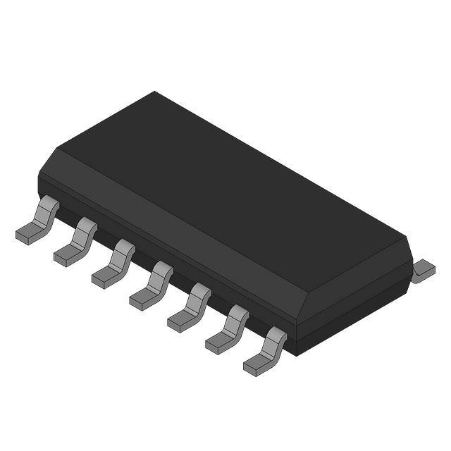


 工商网监
湘ICP备2023018690号
工商网监
湘ICP备2023018690号
