LM330-N
www.ti.com
SNOSC19D – MAY 1998 – REVISED MARCH 2013
LM330-N 3-Terminal Positive Regulator
Check for Samples: LM330-N
FEATURES
1
•
•
•
•
•
•
•
•
2
Input-output Differential Less than 0.6V
Output Current of 150 mA
Reverse Battery Protection
Line Transient Protection
Internal Short Circuit Current Limit
Internal Thermal Overload Protection
Mirror-image Insertion Protection
P+ Product Enhancement Tested
DESCRIPTION
The LM330-N 5V 3-terminal positive voltage regulator
features an ability to source 150 mA of output current
with an input-output differential of 0.6V or less.
Familiar regulator features such as current limit and
thermal overload protection are also provided.
The low dropout voltage makes the LM330-N useful
for certain battery applications since this feature
allows a longer battery discharge before the output
falls out of regulation. For example, a battery
supplying the regulator input voltage may discharge
to 5.6V and still properly regulate the system and
load voltage. Supporting this feature, the LM330-N
protects both itself and regulated systems from
negative voltage inputs resulting from reverse
installations of batteries.
Other protection features include line transient
protection up to 26V, when the output actually shuts
down to avoid damaging internal and external circuits.
Also, the LM330-N regulator cannot be harmed by a
temporary mirror-image insertion.
Schematic and Connection Diagrams
Figure 1. (TO-220)
Plastic Package
Front View
See Package Number NDE0003B
1
2
Please be aware that an important notice concerning availability, standard warranty, and use in critical applications of
Texas Instruments semiconductor products and disclaimers thereto appears at the end of this data sheet.
All trademarks are the property of their respective owners.
PRODUCTION DATA information is current as of publication date.
Products conform to specifications per the terms of the Texas
Instruments standard warranty. Production processing does not
necessarily include testing of all parameters.
Copyright © 1998–2013, Texas Instruments Incorporated
�LM330-N
SNOSC19D – MAY 1998 – REVISED MARCH 2013
www.ti.com
These devices have limited built-in ESD protection. The leads should be shorted together or the device placed in conductive foam
during storage or handling to prevent electrostatic damage to the MOS gates.
Absolute Maximum Ratings (1) (2)
Input Voltage
Operating Range
26V
Line Transient Protection (1000 ms)
40V
Internal Power Dissipation
Internally Limited
Operating Temperature Range
0°C to +70°C
Maximum Junction Temperature
+125°C
−65°C to +150°C
Storage Temperature Range
Lead Temperature
(Soldering, 10 sec.)
(1)
+300°C
“Absolute Maximum Ratings” indicate limits beyond which damage to the device may occur. Operating Ratings indicate conditions for
which the device is functional, but do not ensure specific performance limits.
If Military/Aerospace specified devices are required, please contact the Texas Instruments Sales Office/Distributors for availability and
specifications.
(2)
Electrical Characteristics (1)
Symbol
Vo
ΔVo
Min
Typ
Max
Output Voltage
Parameter
Tj = 25°C
4.8
5
5.2
Output Voltage
5 < Io < 150 mA
4.75
Over Temp
6 < VIN < 26V; 0°C ≤ Tj ≤ 100°C
Line Regulation
9 < VIN < 16V, Io = 5 mA
7
25
6 < VIN < 26V, Io = 5 mA
30
60
5 < Io < 150 mA
14
50
Load Regulation
Conditions
Long Term Stability
IQ
ΔIQ
Quiescent Current
5.25
20
3.5
7
Io = 50 mA
5
11
40
Io = 150 mA
18
VIN = 40V, RL = 100Ω, 1s
14
Reverse Polarity
VIN = −6V, RL = 100Ω
−80
Quiescent Current
6 < VIN < 26V
10
V
mV
mV/1000 hrs
Io = 10 mA
Line Transient
Units
mA
%
Change
VIN
Overvoltage Shutdown
26
38
Voltage
Max Line Transient
60
1s, Vo ≤ 5.5V
50
−30
Reverse Polarity
Input Voltage
DC Vo > − 0.3V, RL = 100Ω
−12
Output Noise Voltage
10 Hz–100 kHz
50
μV
Output Impedance
Io = 100 mADC + 10 mArms
200
mΩ
Ripple Rejection
56
Current Limit
(1)
2
V
150
dB
400
700
0.32
0.6
Dropout Voltage
Io = 150 mA
Thermal Resistance
Junction to Case
4
Junction to Ambient
50
mA
V
°C/W
Unless otherwise specified: VIN = 14V, Io = 150 mA, Tj = 25°C, C1 = 0.1 μF, C2 = 10 μF. All characteristics except noise voltage and
ripple rejection are measured using pulse techniques (tW ≤ 10 ms, duty cycle ≤ 5%). Output voltage changes due to changes in internal
temperature must be taken into account separately.
Submit Documentation Feedback
Copyright © 1998–2013, Texas Instruments Incorporated
Product Folder Links: LM330-N
�LM330-N
www.ti.com
SNOSC19D – MAY 1998 – REVISED MARCH 2013
Typical Performance Characteristics
Dropout Voltage
Dropout Voltage
Figure 2.
Figure 3.
Low Voltage Behavior
High Voltage Behavior
Figure 4.
Figure 5.
Line Transient Response
Load Transient Response
Figure 6.
Figure 7.
Submit Documentation Feedback
Copyright © 1998–2013, Texas Instruments Incorporated
Product Folder Links: LM330-N
3
�LM330-N
SNOSC19D – MAY 1998 – REVISED MARCH 2013
www.ti.com
Typical Performance Characteristics (continued)
4
Peak Output Current
Quiescent Current
Figure 8.
Figure 9.
Quiescent Current
Quiescent Current
Figure 10.
Figure 11.
Ripple Rejection
Ripple Rejection
Figure 12.
Figure 13.
Submit Documentation Feedback
Copyright © 1998–2013, Texas Instruments Incorporated
Product Folder Links: LM330-N
�LM330-N
www.ti.com
SNOSC19D – MAY 1998 – REVISED MARCH 2013
Typical Performance Characteristics (continued)
Output Impedance
Overvoltage Supply Current
Figure 14.
Figure 15.
Reverse Supply Current
Output at Reverse Supply
Figure 16.
Figure 17.
Output at Overvoltage
Output Voltage (Normalized
to 5V at Tj = 25°C)
Figure 18.
Figure 19.
Submit Documentation Feedback
Copyright © 1998–2013, Texas Instruments Incorporated
Product Folder Links: LM330-N
5
�LM330-N
SNOSC19D – MAY 1998 – REVISED MARCH 2013
www.ti.com
TYPICAL APPLICATIONS
The LM330-N is designed specifically to operate at lower input to output voltages. The device is designed
utilizing a power lateral PNP transistor which reduces dropout voltage from 2.0V to 0.3V when compared to IC
regulators using NPN pass transistors. Since the LM330-N can operate at a much lower input voltage, the device
power dissipation is reduced, heat sinking can be simpler and device reliability improved through lower chip
operating temperature. Also, a cost savings can be utilized through use of lower power/voltage components. In
applications utilizing battery power, the LM330-N allows the battery voltage to drop to within 0.3V of output
voltage prior to the voltage regulator dropping out of regulation.
* Required if regulator is located far from power supply filter.
** C2 may be either an Aluminum or Tantalum type capacitor but must be rated to operate at −40°C to ensure
regulator stability to that temperature extreme. 10 μF is the minimum value required for stability and may be increased
without bound. Locate as close as possible to the regulation.
Note: Compared to IC regulator with 2.0V dropout voltage and IQmax, = 6.0 mA.
6
Submit Documentation Feedback
Copyright © 1998–2013, Texas Instruments Incorporated
Product Folder Links: LM330-N
�LM330-N
www.ti.com
SNOSC19D – MAY 1998 – REVISED MARCH 2013
REVISION HISTORY
Changes from Revision C (March 2013) to Revision D
•
Page
Changed layout of National Data Sheet to TI format ............................................................................................................ 6
Submit Documentation Feedback
Copyright © 1998–2013, Texas Instruments Incorporated
Product Folder Links: LM330-N
7
�PACKAGE OPTION ADDENDUM
www.ti.com
10-Dec-2020
PACKAGING INFORMATION
Orderable Device
Status
(1)
Package Type Package Pins Package
Drawing
Qty
Eco Plan
(2)
Lead finish/
Ball material
MSL Peak Temp
Op Temp (°C)
Device Marking
(3)
(4/5)
(6)
LM330T-5.0/NOPB
ACTIVE
TO-220
NDE
3
45
RoHS & Green
SN
Level-1-NA-UNLIM
0 to 70
LM330T
-5.0
(1)
The marketing status values are defined as follows:
ACTIVE: Product device recommended for new designs.
LIFEBUY: TI has announced that the device will be discontinued, and a lifetime-buy period is in effect.
NRND: Not recommended for new designs. Device is in production to support existing customers, but TI does not recommend using this part in a new design.
PREVIEW: Device has been announced but is not in production. Samples may or may not be available.
OBSOLETE: TI has discontinued the production of the device.
(2)
RoHS: TI defines "RoHS" to mean semiconductor products that are compliant with the current EU RoHS requirements for all 10 RoHS substances, including the requirement that RoHS substance
do not exceed 0.1% by weight in homogeneous materials. Where designed to be soldered at high temperatures, "RoHS" products are suitable for use in specified lead-free processes. TI may
reference these types of products as "Pb-Free".
RoHS Exempt: TI defines "RoHS Exempt" to mean products that contain lead but are compliant with EU RoHS pursuant to a specific EU RoHS exemption.
Green: TI defines "Green" to mean the content of Chlorine (Cl) and Bromine (Br) based flame retardants meet JS709B low halogen requirements of
很抱歉,暂时无法提供与“LM330T-5.0/NOPB”相匹配的价格&库存,您可以联系我们找货
免费人工找货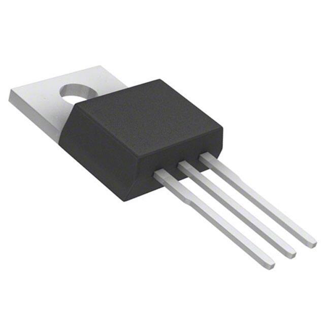


 工商网监
湘ICP备2023018690号
工商网监
湘ICP备2023018690号
