LM3432, LM3432B
www.ti.com
SNVS498D – APRIL 2007 – REVISED MAY 2013
6-Channel Current Regulator for LED Backlight Application
Check for Samples: LM3432, LM3432B
FEATURES
•
1
•
2
•
•
•
•
•
•
•
•
•
Dynamic Headroom Control (DHC) Output to
Maximize Efficiency when used in Conjunction
with Texas Instruments Semiconductor's
LM3430 Boost Controller for LED Backlighting
Current Sinking Adjustable up to 40mA in
Each String
Fast Current Switching Slew Rate, tr = 60ns
Typical
Wide Dimming Ratio, up to 4000:1 with fDIM =
500Hz
High LED Driving Voltage up to 80V
±2.0% Current Matching Between Strings
Accepts Both Digital and Analog Dimming
Control
LED Open/Short Fault Indication (For
LM3432B, no open fault indication)
Over-Temperature Indication
Internal Thermal Shutdown with Hysteresis
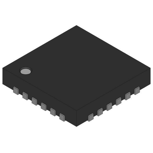
Low profile, Thermally Enhanced WQFN-24
(5x4x0.8mm) and eHTSSOP-28
(9.7x6.4x1.1mm) Packages (The LM3432B is
available in the WQFN-24 only)
APPLICATIONS
•
•
LCD Display Backlight Applications
General Lighting Solutions
DESCRIPTION
The LM3432/LM3432B are 6-channel high voltage
current regulators which provide a simple solution for
LED
backlight
applications.
These
devices
incorporate six individual current regulator channels
to give accurate driving current for each LED string.
The string-to-string tolerance is kept within ±2.0%.
Additionally, the Dynamic Headroom Control output
can communicate with a LM3430 boost regulator to
adjust the LED supply voltage to the lowest level
needed to keep the string current in regulation,
yielding optimal overall system efficiency.
TYPICAL APPLICATION CIRCUIT
Adjust to the lowest possible
voltage level to maximize
efficiency
VLED+
( 80V max. )
VIN
CVIN
Connect to GND
for digital input/
Connect with
capacitor for
analog input
To LM3430
VDHC pin
MODE
VIN
RDHC
VDHC
CDHC
CDHC
CVDHC
LM3432/LM3432B
VCC
IREF
CVCC
IOUT1
IOUT2
RIREF
IOUT3
IOUT4
IOUT5
PWM for digital input/
DC voltage for analog input
DIM
OTMb
EN
ON
OFF
IOUT6
AGND PGND
FAULTb
Fault logics
to MCU
GND
1
2
Please be aware that an important notice concerning availability, standard warranty, and use in critical applications of
Texas Instruments semiconductor products and disclaimers thereto appears at the end of this data sheet.
All trademarks are the property of their respective owners.
PRODUCTION DATA information is current as of publication date.
Products conform to specifications per the terms of the Texas
Instruments standard warranty. Production processing does not
necessarily include testing of all parameters.
Copyright © 2007–2013, Texas Instruments Incorporated
�LM3432, LM3432B
SNVS498D – APRIL 2007 – REVISED MAY 2013
www.ti.com
DESCRIPTION CONTINUED
The 6-channel current sink can be adjusted from 15mA to 40mA by an external resistor. Their output drivers can
withstand up to 80V. Digital PWM or analog voltage signal can be used to control the duty cycle of all the
channels. With a fast current switching slew rate, tr = 60ns typical, accurate current control and wide dimming
ratio during PWM dimming are ensured.
The LM3432/LM3432B contain LED open/short circuit and over-temperature fault signaling to the system microcontroller (the LM3432B does not include open circuit fault signaling). These devices are available in a low
profile, thermally enhanced 24 lead WQFN package. The LM3432 is also available in the 28 lead eHTSSOP.
IOUT1
20
PGND
VIN
NC
21
22
23
24
NC
Connection Diagram
VCC
1
IREF
2
18
NC
AGND
3
17
IOUT3
19
IOUT2
CDHC
4
16
NC
VDHC
5
15
IOUT4
EN
6
14
NC
EP
12
IOUT5
IOUT6
11
NC
OTMb
FAULTb
DIM
10
13
9
7
8
MODE
Figure 1. Top View
24 Lead Plastic WQFN-24
VIN
1
28
PGND
NC
2
27
PGND
NC
3
26
NC
NC
4
25
IOUT1
VCC
5
24
NC
IREF
6
23
IOUT2
AGND
7
22
NC
CDHC
8
21
IOUT3
VDHC
9
20
NC
EN
10
19
IOUT4
MODE
11
18
NC
DIM
12
17
IOUT5
FAULTb
13
16
NC
OTMb
14
15
IOUT6
EP
Figure 2. Top View
28 Lead Plastic eHTSSOP-28
Pin Descriptions
Pin Number
2
WQFN-24
eHTSSOP-28
1
5
2
3
Name
Description
VCC
Internal linear regulator output, needs 680nF minimum for stability.
6
IREF
IOUT current setting pin. An external resistor is used to program the string current.
7
AGND
Analog ground
4
8
CDHC
An external capacitor to ground programs the Dynamic Headroom Control (DHC)
response time constant.
5
9
VDHC
DHC voltage output. Connecting this output through a gain setting resistor to the DHC
pin of Texas Instruments Semiconductor's LM3430 enables the DHC function.
6
10
EN
7
11
MODE
8
12
DIM
9
13
FAULTb
Device Enable, active HIGH.
Dimming mode select pin. Short to ground for Digital PWM dimming or connect to an
external capacitor to ground for analog dimming.
Digital PWM or Analog voltage input for IOUT duty cycle.
Open drain active LOW output for output fault.
10
14
OTMb
12, 13, 15,
17, 19, 20
15, 17, 19,
21, 23, 25
IOUT1-6
Open drain active LOW over temperature warning output.
22
27, 28
PGND
24
1
VIN
Supply voltage input, from 6V to 40V.
11, 14, 16,
18, 21, 23
2, 3, 4, 16, 18,
20, 22, 24, 26
NC
No connection and should be left open.
EP
EP
EP
Thermal connection pad, connect directly to GND.
Constant current sink outputs, adjustable 15mA to 40mA, voltage across this pin can
be up to 80V max.
Power Ground.
Submit Documentation Feedback
Copyright © 2007–2013, Texas Instruments Incorporated
Product Folder Links: LM3432 LM3432B
�LM3432, LM3432B
www.ti.com
SNVS498D – APRIL 2007 – REVISED MAY 2013
These devices have limited built-in ESD protection. The leads should be shorted together or the device placed in conductive foam
during storage or handling to prevent electrostatic damage to the MOS gates.
ABSOLUTE MAXIMUM RATINGS
(1) (2)
If Military/Aerospace specified devices are required, contact the Texas Instruments Sales Office/ Distributors for
availability and specifications.
VALUE / UNIT
VIN Voltage
-0.3V to 42V
IREF Voltage
-0.3V to 7V
IOUT1 through IOUT6 Voltage
-0.3V to 82V
VCC Voltage
-0.3V to 7V
EN Voltage
-0.3V to 7V
FAULTb, OTMb Voltage
-0.3V to 7V
MODE Voltage
-0.3V to 7V
PWM Voltage
-0.3V to 7V
VDHC Voltage
-0.3V to 7V
CDHC Voltage
-0.3V to 7V
ESD Susceptibility
Human Body Model
(3)
2.0kV
Lead Temperature
Vapor Phase (60 sec.)
215°C
Infra-red (15 sec.)
220°C
Maximum Junction Temperature
(1)
(2)
(3)
150°C
Absolute Maximum Ratings are limits beyond which damage to the device may occur. The Recommended Operating Limits define the
conditions within which the device is intended to be functional. For specifications and test conditions, see the Electrical Characteristics.
Rating limits apply to both the LM3432 and LM3432B.
The human body model is a 100 pF capacitor discharged through a 1.5kΩ resistor into each pin.
RECOMMENDED OPERATING CONDITIONS
(1)
VALUE / UNIT
Supply Voltage, VIN
6 to 40V
IOUT1 through IOUT6 Voltage
0 to 80V
Operating Junction Temp.
-40°C to +125°C
Storage Temperature
Thermal Resistance, θJA
-65°C to +150°C
(2)
WQFN-24
eHTSSOP-28
(1)
(2)
33.2°C/W
29°C/W
Absolute Maximum Ratings are limits beyond which damage to the device may occur. The Recommended Operating Limits define the
conditions within which the device is intended to be functional. For specifications and test conditions, see the Electrical Characteristics.
The maximum allowable power dissipation is a function of the maximum junction temperature, TJ_MAX, the junction-to-ambient thermal
resistance, θJA and the ambient temperature, TA. The maximum allowable power dissipation at any ambient temperature is calculated
using: PD_MAX = (TJ_MAX - TA)/θJA. Exceeding the maximum allowable power dissipation will cause excessive die temperature.
Submit Documentation Feedback
Copyright © 2007–2013, Texas Instruments Incorporated
Product Folder Links: LM3432 LM3432B
3
�LM3432, LM3432B
SNVS498D – APRIL 2007 – REVISED MAY 2013
www.ti.com
ELECTRICAL CHARACTERISTICS
Limits in standard type are for TJ = 25°C only; limits in boldface type apply over the junction temperature (TJ) range of -40°C
to +125°C. Minimum and Maximum limits are specified through test, design, or statistical correlation. VIN = 18V, RIREF = 54.7
kΩ, VEN = 5V, VMODE = 0V, VDIM = 5V and VOUT1-6 = 1.2V unless otherwise indicated (1). Parameter limits apply to both the
LM3432 and LM3432B unless otherwise indicated.
Symbol
Parameter
Conditions
Min
Typ
Max
Units
Input Characteristics
ISHDN
IQ
VEN
VEN_HYST
IEN
Shutdown Input Supply Current
EN = 0V, DIM = 0V
Quiescent Current from VIN
Enable Threshold Voltage
VEN rising
1.48
Enable Threshold Hysteresis
Enable pin Pull-up Current
40
90
µA
2.25
2.65
mA
1.75
2
V
0.4
V
EN = 0V
0.5
µA
EN = 2V
5
VCC Regulator
VCCreg
VCC Regulated Output
4.7
5
5.25
V
4.7
5
5.25
V
VCCreg_1
VCC Regulated Output at Max. VIN
VIN = 40V
VCCreg_2
VCC Regulated Output at Min. VIN
VIN = 6V, IVCC = 2mA
4.8
V
IVCC_SC
VCC Short-Circuit Current
VIN = 6V, VCC = 0V
9
mA
VCCUVLO
VCC UVLO Upper Threshold
VCC rising
VCCUVLO_HYST
3.9
VCC UVLO Hysteresis
4.15
4.4
V
0.375
V
Analog PWM control
IMODE
MODE pin Output Current
MODE = 2V
34
µA
VMODE_PK
MODE pin Peak Voltage
CMODE = 5.6nF
3.1
V
VMODE_VA
MODE pin Valley Voltage
CMODE = 5.6nF
1.0
V
Digital PWM control
VPWM_HIGH
PWM Voltage HIGH
MODE = GND
VPWM_LOW
PWM Voltage LOW
MODE = GND
1.7
V
1
V
Dynamic Headroom Control Output
VDHC_MAX
VDHC pin Max. Output Voltage
IVDHC = 2mA
2
IVDHC_MAX
5
2.5
V
VDHC pin Max. Output Current
VDHC = 1.2V
9
mA
VDHC_REG_20
VDHC Regulation at 20mA
RIREF = 54.7k, CDHC = 100nF
0.625
V
VDHC_REG_40
VDHC Regulation at 40mA
RIREF = 27.5k, CDHC = 100nF
1.25
V
IOUT Rising Edge Phase Delay
MODE = GND, Pulsing PWM 10µs
500
ns
IOUT Rise Time
MODE = GND, rising edge from 10%
to 90% of IOUT
25
ns
Switching Characteristics
tpd_H
Tr
Output Current
VIREF
IREF pin Voltage
6V ≤ VIN ≤ 40V
1.215
1.245
1.27
V
IOUT20
Constant Current Sink of 20mA
RIREF = 54.7k, VIOUT1-6 = 1.1V
18.85
18.5
20
21.05
21.4
mA
IOUT40
Constant Current Sink of 40mA
RIREF = 27.5k, VIOUT1-6 = 1.6V
37.9
37.3
40
41.55
42.15
mA
Output Current Matching of IOUT20 (2)
6V ≤ VIN ≤ 40V
2.25
%
IOUT20_match
(1)
(2)
All limits are specified at room temperature (standard type face) and at temperature extremes (bold type face). All room temperature
limits are 100% tested. All limits at temperature extremes are ensured via correlation using standard Statistical Quality Control (SQC)
methods. All limits are used to calculate Average Outgoing Quality Level (AOQL). Typical values represent the most likely parametric
norm at TJ = 25°C and are provided for reference purposes only.
IOUT_match is the greatest percentage delta between output string currents with respect to the median.
1 Max(IOUTX) - Min(IOUTX)
x 100% and
IOUT_match =
2
Median
Median =
4
Max(IOUTX) + Min(IOUTX)
2
Submit Documentation Feedback
Copyright © 2007–2013, Texas Instruments Incorporated
Product Folder Links: LM3432 LM3432B
�LM3432, LM3432B
www.ti.com
SNVS498D – APRIL 2007 – REVISED MAY 2013
ELECTRICAL CHARACTERISTICS (continued)
Limits in standard type are for TJ = 25°C only; limits in boldface type apply over the junction temperature (TJ) range of -40°C
to +125°C. Minimum and Maximum limits are specified through test, design, or statistical correlation. VIN = 18V, RIREF = 54.7
kΩ, VEN = 5V, VMODE = 0V, VDIM = 5V and VOUT1-6 = 1.2V unless otherwise indicated (1). Parameter limits apply to both the
LM3432 and LM3432B unless otherwise indicated.
Symbol
IOUT40_match
IOUT_max
Parameter
Conditions
Output Current Matching of IOUT40
(2)
Min
Typ
Max
2
%
50
80
110
mA
V
6V ≤ VIN ≤ 40V
Units
Maximum Output Current, IREF shorted to
GND.
VIREF = 0V, VIOUT = 4.5V
VDROP_IOUT20
Dropout Voltage of IOUT20 (3)
RIREF = 54.7k
0.3
0.525
VDROP_IOUT40
Dropout Voltage of IOUT40 (3)
RIREF = 27.5k
0.6
1.125
V
Output Current when EN is LOW
EN = 0, VOUT = 80V
0.025
3
µA
VSHORTFAULT
VIOUT Short Fault Threshold
FAULTb goes LOW during VIOUT
rising,
Other VIOUTs = 1.0V
7.9
8.8
V
tD_SHORTFAULT
Short Fault Delay
VIOUT set to 10V, FAULTb goes LOW,
Other VIOUTs = 1.0V
150
tD_OPENFAULT
Open Fault Delay (LM3432 only)
VIOUTX set open, FAULTb goes LOW
50
VFAULT_LOW
FAULTb and OTMb LOW
5mA into FAULTb
ILEAK_FAULT
FAULTb and OTMb Open Leakage
VFAULTb = VOTMb = 5V
IOUT_OFF
Fault Detection
7.3
0.005
µs
µs
0.7
V
1
µA
Thermal Protection
(3)
OTM
Over Temperature Monitor Threshold
125
°C
OTMHYST
Over Temperature Monitor Hysteresis
20
°C
TSD
Thermal Shutdown Threshold
165
°C
TSDHYST
Thermal Shutdown Hysteresis
20
°C
Dropout voltage is defined as the IOUT pin to GND voltage at which the output current sink drops 10% from the nominal value.
Submit Documentation Feedback
Copyright © 2007–2013, Texas Instruments Incorporated
Product Folder Links: LM3432 LM3432B
5
�LM3432, LM3432B
SNVS498D – APRIL 2007 – REVISED MAY 2013
www.ti.com
TYPICAL PERFORMANCE CHARACTERISTICS
Unless otherwise specified, the following conditions apply: VIN = 18V, RIREF = 54.7 kΩ, VEN = 5V, VMODE = 0V, VDIM = 5V and
VOUT1-6 = 1.2V. Typical performance characteristics are valid for both the LM3432 and LM3432B unless otherwise indicated.
Quiescent Current vs Supply Voltage
Shutdown Current vs Supply Voltage
10
100
8
80
ISHDN (PA)
IQ (mA)
125°C
6
4
-40°C
-40°C
60
+25°C
40
125°C
2
20
+25°C
0
0
0
10
20
30
40
50
0
10
20
VIN (V)
30
40
50
VIN (V)
Figure 3.
Figure 4.
VCC Regulator Output vs Supply Voltage
Current Setting Reference Voltage vs Supply Voltage
5.1
1.27
IVCC = 2mA
1.26
+25°C
VIREF (V)
VCCreg (V)
5.05
-40°C
5
+25°C
1.25
125°C
1.24
-40°C
4.95
125°C
1.23
4.9
1.22
0
10
20
30
40
50
0
10
20
VIN (V)
30
40
50
VIN (V)
Figure 5.
Figure 6.
Average String Current vs Current Setting Resistance
Output Current Matching vs Temperature
3.0
50
VIN = 18V
IOUT_match (%)
IOUT(AVG) (mA)
40
30
-40°C
2.0
RIREF = 73.3 k:
RIREF = 54.7 k:
1.0
+25°C
20
RIREF = 27.5 k:
125°C
10
20
30
40
50
60
70
80
0.0
-50
50
100
150
TJ (°C)
RIREF (k:)
Figure 7.
6
0
Figure 8.
Submit Documentation Feedback
Copyright © 2007–2013, Texas Instruments Incorporated
Product Folder Links: LM3432 LM3432B
�LM3432, LM3432B
www.ti.com
SNVS498D – APRIL 2007 – REVISED MAY 2013
TYPICAL PERFORMANCE CHARACTERISTICS (continued)
Unless otherwise specified, the following conditions apply: VIN = 18V, RIREF = 54.7 kΩ, VEN = 5V, VMODE = 0V, VDIM = 5V and
VOUT1-6 = 1.2V. Typical performance characteristics are valid for both the LM3432 and LM3432B unless otherwise indicated.
PWM Digital Dimming Operation
(Channel 1 Waveform)
PWM Dimming Frequency vs CMODE
60
50
fDIM (kHz)
40
30
20
10
0
100
1000
10000
100000
CMODE (pF)
Figure 9.
Figure 10.
PWM Dimming Characteristic, Rising Edge
(Channel 1 Waveform)
PWM Dimming Characteristic, Falling Edge
(Channel 1 Waveform)
Figure 11.
Figure 12.
Analog Dimming Operation
Figure 13.
Submit Documentation Feedback
Copyright © 2007–2013, Texas Instruments Incorporated
Product Folder Links: LM3432 LM3432B
7
�LM3432, LM3432B
SNVS498D – APRIL 2007 – REVISED MAY 2013
www.ti.com
SIMPLIFIED FUNCTIONAL BLOCK DIAGRAM
VIN
VIN
5V LINEAR
REGULATOR
vcc
VIN
BANDGAP
THERMAL
SHUTDOWN
EN
vcc
VCC
VDHC
vcc
AGND
IREF
vcc
FAULT
IREF
IREF
PGND
vcc
vcc
IREF
VDHC
MODE
FAULT
DIM
IOUT1
ON
IOUT2
ON
FAULT
6
CONTROL
vcc
ON
6
CDHC
IREF
IOUT3
ON
FAULT
FAULTb
vcc
IREF
IOUT4
ON
FAULT
vcc
IREF
vcc
OTMb
IOUT5
ON
FAULT
OVER-TEMP
vcc
IREF
IOUT6
ON
FAULT
8
Submit Documentation Feedback
Copyright © 2007–2013, Texas Instruments Incorporated
Product Folder Links: LM3432 LM3432B
�LM3432, LM3432B
www.ti.com
SNVS498D – APRIL 2007 – REVISED MAY 2013
FUNCTIONAL DESCRIPTION
OVERVIEW
The LM3432/LM3432B are 6-channel high voltage current regulators for LED backlight applications which
incorporates individual channel current regulators to give accurate current sinking for each LED string. String to
string tolerance is kept within ±2.0% at 40 mA and ±2.25% at 20 mA. The 6-channels current sinks can be
adjusted from 15 mA to 40 mA by an external resistor. Channel outputs can withstand up to 80V. Channel 5 or 6
output can be disabled by shorting the selected output pin to ground prior to power-up. Both the digital PWM
dimming signal and analog voltage signal can be used to control the duty cycle of all the six channels. The
LM3432/LM3432B also provide fault indications to the system MCU for an LED open (included in the LM3432
only) or short circuit or an over-temperature condition.
INTERNAL 5V LINEAR REGULATOR
An internal 5V linear regulator with an Under-Voltage Lock-Out (UVLO) function is integrated within the
LM3432/LM3432B. This regulated 5V is used for internal circuitry and can support a small amount of external
loading, not to exceed 2 mA when VIN = 6V. The supply input pin (VIN) can be connected directly to an input
voltage up to 40V, with transient capability up to 42V. The VCC output regulates at 5V and is current limited to 9
mA. To ensure stable operation, the external capacitor CVCC must be at least 680 nF with 1 µF recommended. If
the voltage at the VCC pin drops below the UVLO threshold of 3.8V, the device will shut down the output
channels and other functional blocks. Normal operation will be resumed once the VCC voltage is allowed to rise
above the UVLO rising threshold of 4.15V.
BANDGAP VOLTAGE REFERENCE
A precision reference voltage is required for accurate control of the output currents. The LM3432/LM3432B
contain a bandgap voltage reference block that provides a high precision reference voltage for internal operation.
The bandgap reference voltage is typically trimmed to 1.245V.
OUTPUT CURRENT REGULATOR (IOUT1 to IOUT6)
The LM3432/LM3432B contains six individual integrated current regulators to give accurate current sinking for
each LED string. String to string tolerance is kept within ±2.0% at 40 mA and ±2.25% at 20 mA. The sink current
level is adjusted by an external resistor, RIREF in the range of 15 mA to 40 mA. The IOUT pins can withstand up
to 80V. The ability to withstand high voltage enables the user to add more LEDs in a single string. The
calculation of IOUT with respect to RIREF is shown below.
1.094
x 106 where IOUT is in mA
IOUT =
RIREF
(1)
Channels 5 and 6 are designed to be user disabled without activating the fault detection circuitry. With this
feature, the user can readily configure the device to a 4, 5 or 6 channel driver. In order to disable a channel, the
IOUT5 and/or IOUT6 pin(s) must be tied to ground before powering up the device. During power-up, channels 5
and 6 will be checked and any grounded channel(s) will be automatically disabled. The disabled status will
remain until either power is recycled or the enable (EN) pin is toggled.
ANALOG DIMMING OF LED STRINGS
Dimming of LED brightness is achieved by Pulse Width Modulation (PWM) control of the string currents. The
LM3432/LM3432B accepts both analog voltage and PWM digital dimming input signals for this feature. With a
capacitor (CMODE) connected across the MODE pin and ground, the device will monitor the voltage level at the
DIM pin and generate the required PWM control signal internally. The internal implementation of the
LM3432/LM3432B’s dimming function is illustrated in Figure 14.
Submit Documentation Feedback
Copyright © 2007–2013, Texas Instruments Incorporated
Product Folder Links: LM3432 LM3432B
9
�LM3432, LM3432B
SNVS498D – APRIL 2007 – REVISED MAY 2013
www.ti.com
DIM
1V to 3V +
-
PWM
+
Comp2
-
VDIM
VCC
PWM
Modulator
34 PA
MODE
+
Comp1
-
3V
1V
3V
+
-
CMODE
+
1V
Ramp
Generator
-
Figure 14. Analog Dimming of LEDs
An internal current source of 34 µA (typical) will charge the external capacitor (CMODE) linearly until it reaches 3V.
The comparator (Comp1) then forces CMODE to be discharged to 1V very quickly. By repeating the cycle, a sawtooth waveform as shown in Figure 14 is generated. Comparator (Comp2) compares this ramp waveform with
the external dc voltage at the DIM pin generating the desired PWM control signal.
When VDIM ≤ 1V, ON duty factor, DON = 0% and when VDIM ≥ 3V, DON = 100%. The frequency of the PWM
control signal can be calculated as shown below.
fPWM =
1.65 x 10⁻⁵
where fPWM is in Hz
CMODE
(2)
Or
CMODE =
1.65 x 10⁻⁵
where CMODE is in Farads
fPWM
(3)
PWM DIGITAL DIMMING of LED STRINGS
Alternatively, the dimming control can be implemented by direct application of a digital signal to the device. With
the MODE pin connected to ground, an externally applied PWM dimming signal is applied to the DIM pin. The
peak amplitude of the externally applied PWM signal should be greater than 1.5V to ensure clean PWM
switching.
During PWM dimming, channels are not switched simultaneously in an effort to minimize large surge currents
from being drawn from the LED supply rail. Each channel will have 0.5 µs phase delay with respect to the
preceding channel. As a consequence of the phase delay, for a control pulse width less than 0.5 µs, the duty
cycle will be rounded down to 0% and for a control pulse width less than 0.5 µs off time, the duty cycle will be
rounded up to 100%. Therefore, 0.5µs becomes the finest pulse width resolution that can be realized. The PWM
switching timing for all six channels is shown in Figure 15.
10
Submit Documentation Feedback
Copyright © 2007–2013, Texas Instruments Incorporated
Product Folder Links: LM3432 LM3432B
�LM3432, LM3432B
www.ti.com
SNVS498D – APRIL 2007 – REVISED MAY 2013
T = TON + TOFF
VDIM
TON
TOFF
IOUT1
0.5 Ps
IOUT2
1.0 Ps
IOUT3
1.5 Ps
IOUT4
2.0 Ps
IOUT5
2.5 Ps
IOUT6
3.0 Ps
Time
Figure 15. PWM Dimming Switching Timing
LED SHORT FAULT DETECT
With DHC
If the Dynamic Headroom Control (DHC) feature is used, the lowest voltage between the IOUT pins and ground
among the strings will be regulated to 0.625V typical (ILED = 20 mA) by lowering the LED supply rail voltage,
VLED. If an LED short fault condition occurs and causes the voltage between any of the IOUT pins and ground to
exceed the typical short fault threshold of 7.9V for more than 150 µs, the affected channel(s) will be latched off
and the FAULTb pin will be pulled to ground. The affected channel(s) will remain latched off until recycling power
or toggling the EN pin. All of the other channels that are not affected will continue to function normally.
Without DHC
In applications where the DHC function is not used, the IOUT pin voltage on each string will be the voltage
difference between the LED supply rail voltage, VLED, and the voltage drop across the entire LED string. If the
voltage between any of the IOUT pins and ground is less than 2V typical, the short fault detect feature will be
active for all channels. In the event an LED short fault condition occurs and causes the voltage between any of
the IOUT pin and ground to exceed the typical short fault threshold of 7.9V for more than 150 μs, the affected
channel(s) will be latched off and the FAULTb pin will be pulled to ground. The affected channel(s) will remain
latched off until recycling power or toggling the EN pin. All of the other channels that are not affected will
continue to function normally. If the voltages between all IOUT pins and ground are greater than 2V typical, the
Short Fault Detect feature will be disabled to prevent false triggering of the short fault detect function.
Submit Documentation Feedback
Copyright © 2007–2013, Texas Instruments Incorporated
Product Folder Links: LM3432 LM3432B
11
�LM3432, LM3432B
SNVS498D – APRIL 2007 – REVISED MAY 2013
www.ti.com
LED OPEN FAULT DETECT (LM3432 ONLY)
For the LM3432, if an open fault should occur and the affected channel sinks no current for greater than 50 µs, it
will be latched off (until recycling power or toggling EN pin). The FAULTb pin’s output will be pulled to ground
while the other channels keep functioning normally. The open fault detection and FAULTb indication features are
inactive in the LM3432B.
IOUT
#
SHORT FAULT
6V
P(M
+
VCC
ShortFaultx
VIREF
ON
V
-
+ -
+
FAULT
#
IOUTx Driver
VCC
+ -
0.3V
+
OpenFaultx
** OPEN FAULT
** Open fault protection and indication are not available in the LM3432B
Figure 16. Fault Detect Functional Block Diagram
OVER-TEMPERATURE MONITOR
If the LM3432/LM3432B junction temperature exceeds approximately 125°C, the OTMb pin will be pulled to
ground but the part will continue to function. Action must be taken to lower the temperature at this point. The
PWM duty factor may be lowered as an example to reduce the amount of heat generated, which will in turn lower
the die temperature. If the junction temperature is allowed to rise beyond approximately 165°C, the part will shut
down. When the device is cooled down to about 145°C, device operation will resume.
Note that this thermal shutdown protection is only intended as a fault mode protection feature. Device operation
above rated maximum operating junction temperature is neither recommended nor ensured.
12
Submit Documentation Feedback
Copyright © 2007–2013, Texas Instruments Incorporated
Product Folder Links: LM3432 LM3432B
�LM3432, LM3432B
www.ti.com
SNVS498D – APRIL 2007 – REVISED MAY 2013
DYNAMIC HEADROOM CONTROL
To use the DHC function, connect a gain setting resistor from the VDHC pin of the LM3432/LM3432B to the
VDHC pin of the LM3430 (Texas Instruments Semiconductor’s Boost Controller for LED Backlighting) that is
supplying power to the LED rails. The LM3432/LM3432B’s DHC function will regulate the voltage between the
IOUT pins and ground to a minimum of 0.625V typical (IOUT = 20 mA) to optimize overall efficiency. A large
DHC time constant needs to be set in order not to interfere with the loop response of the DC-DC converter. This
can be implemented by connecting a capacitor from the LM3432/LM3432B’s CDHC pin to ground. If the DHC
function is not needed, leave the VDHC pin floating. When operated in this manner, if the lowest voltage between
any of the IOUT pins and ground is greater than 2V, the LED short fault detection function will be disabled. For
the LM3432B, if any open condition occurs on any channels, the DHC function will be inactive and the LED
supply rail voltage from the LM3430 will stay at its preset level. If the excess headroom voltage is greater than
the short fault detect threshold, 7.3V(min), the device may latch off the LED string(s) due to short fault protection.
In order to insure the proper operation of good LED strings, designers must design for sufficient excess
headroom voltage below the short fault detect threshold.
Submit Documentation Feedback
Copyright © 2007–2013, Texas Instruments Incorporated
Product Folder Links: LM3432 LM3432B
13
�LM3432, LM3432B
SNVS498D – APRIL 2007 – REVISED MAY 2013
www.ti.com
APPLICATIONS INFORMATION
The LM3432/LM3432B provide a simple and handy solution for LED driving. With only a few external passive
components, an LED panel of up to about 120 white LEDs can be illuminated. A typical application configuration
driving six strings with twelve white LEDs per string is shown in Figure 17.
VLED = 48V
VIN = 6V ± 40V
12 LEDs / String
CVIN
1 PF/50V
FAULTb
Fault flags to MCU
VIN
OTMb
VDHC
CDHC
MODE
LM3432/LM3432B
CVCC
RIREF
1 PF/10V
54.7k
VLED+
IOUT1
VCC
IREF
IOUT1
IOUT2
IOUT2
IOUT3
IOUT3
IOUT4
PWM digital dimming
control input
IOUT4
IOUT5
DIM
IOUT5
> +1.5V
IOUT6
IOUT6
ON
EN
AGND
PGND
OFF
GND
Figure 17. Typical Application Schematic to Drive 72 White LEDs (@20 mA) (PWM Digital Dimming)
DETERMINATION OF EXTERNAL COMPONENTS
The typical application only requires three external components. The selection of those components is described
in detail below.
Programming of String Current, IOUT1 to IOUT6
The string current can be programmed by an external resistor, RIREF. The equation to calculate the resistance of
this resistor is shown below.
1.094
in k:
RIREF =
IOUT
(4)
In order to ensure good current regulation over the full operating temperature range, a high quality resistor with
±1% tolerance and a low temperature coefficient is recommended.
14
Submit Documentation Feedback
Copyright © 2007–2013, Texas Instruments Incorporated
Product Folder Links: LM3432 LM3432B
�LM3432, LM3432B
www.ti.com
SNVS498D – APRIL 2007 – REVISED MAY 2013
For the example shown in Figure 17, the string current is 20 mA. Applying to the equation:
1.094
= 54.7 k:
RIREF =
20 mA
(5)
Selecting the VCC Output Capacitor, CVCC
For proper operation, a VCC output capacitor (CVCC) of at least 680 nF is required for stability reason. The
recommended CVCC capacitance is 1 µF.
Selecting the VIN Capacitor, CVIN
The purpose of this capacitor is to supply transient current to the device and suppress VIN noise in order to
ensure proper operation. A low ESR ceramic capacitor with good high frequency performance is recommended.
The capacitance can range from 0.1 µF to 1 µF.
Analog Dimming Control
If analog dimming control is required, a capacitor, CMODE should be connected from the MODE pin to ground
instead of shorting the MODE pin to ground. The relationship between the PWM dimming frequency and the
capacitance of CMODE is illustrated below.
fPWM =
1.65 x 10⁻⁵
CMODE
where CMODE is in Farads and fPWM is in Hz
(6)
When VPWM ≤ 1V, DON = 0% and when VPWM ≥ 3V, DON = 100%
The LED dimming ratio is calculated from the ratio of minimum ON duty factor to the maximum ON duty factor.
With the LM3432/LM3432B, the LEDs can be fully turned on up to 100% ON duty factor and the minimum ON
duty factor is limited by the phase delay time, 0.5 µs. The dimming ratio can be estimated as below.
Dimming Ratio =
1
:1
5 x 10⁻⁷ fPWM
(7)
As an example, if the PWM dimming frequency is set to 500 Hz, the best achievable dimming ratio is:
Dimming Ratio (fPWM = 500 Hz) =
1
-7
5 x 10 x 500
: 1 = 4000 : 1
(8)
Driving High Current LEDs
The LM3432/LM3432B can support string currents from 15 mA to 40 mA. If the application needs to drive high
current LEDs that require more than 40 mA per string, the LM3432/LM3432B provides the alternative of
connecting several IOUT ports together to achieve higher output current per string. With this approach, there is
the obvious trade off between higher output current and number of strings driven. Two possible configurations
are illustrated in Figure 18.
Submit Documentation Feedback
Copyright © 2007–2013, Texas Instruments Incorporated
Product Folder Links: LM3432 LM3432B
15
�LM3432, LM3432B
CVIN
VLED = 50V
VIN = 6V ± 40V
CVIN
1 PF/50V
12 LEDs/String
VLED = 50V
VIN = 6V ± 40V
www.ti.com
12 LEDs/String
SNVS498D – APRIL 2007 – REVISED MAY 2013
1 PF/50V
VIN
VIN
LM3432/
LM3432B
LM3432/
LM3432B
VLED+
IOUT1
IOUT1
IOUT2
IOUT2
IOUT2
IOUT3
IOUT4
IOUT5
IOUT2
IOUT3
IOUT3
IOUT3
IOUT4
IOUT4
IOUT4
IOUT5
IOUT5
IOUT5
IOUT6
IOUT6
IOUT6
AGND
VLED+
IOUT1
IOUT1
IOUT6
PGND
AGND
PGND
40 mA Per channel
40 mA Per channel
GND
GND
Two 120 mA Strings
Three 80 mA Strings
Figure 18. Achieving Higher LED String Current by Grouping IOUT Ports
Dynamic Headroom Control, DHC with LM3430
When the LM3432/LM3432B are powered with Texas Instruments Semiconductor's Boost Controller for LED
Backlighting, LM3430, the Dynamic Headroom Control (DHC) feature helps to provide the optimal system
efficiency. By connecting VDHC through a gain setting resistor to the DHC pin of the LM3430 that is supplying
the LED power rail, the LM3432/LM3432B’s DHC function will regulate the minimum of the ON voltage of the six
channels to 0.625V typical (IOUT = 20 mA). This is the minimum voltage headroom required at outputs to keep the
current regulator in its linear operating range. In order not to interfere with the feedback loop response of the
upstream DC-DC converter, the DHC response time constant must be set to a large enough value by adding a
capacitor from CDHC pin to ground.
Figure 19 is an application schematic of a LED panel driver using both the LM3430 and the LM3432/LM3432B
with the Dynamic Headroom Control function enabled. The LM3430 boosts a voltage from VIN to 50V nominal to
supply the LED strings. With the DHC function disabled, the LM3430 will keep the LED string supply regulated at
50V. When the DHC is enabled, this voltage will dynamically be regulated down to a voltage that can just keep
all LED string currents in regulation. That is about 40V in the application shown in Figure 19. The reduction in
this rail voltage can significantly improve the overall system efficiency.
16
Submit Documentation Feedback
Copyright © 2007–2013, Texas Instruments Incorporated
Product Folder Links: LM3432 LM3432B
�LM3432, LM3432B
www.ti.com
SNVS498D – APRIL 2007 – REVISED MAY 2013
RUV2
182k
VIN
8V~26V
VIN
CIN1
10 PF
50V
CCOMP2 12 pF
FB
COMP
VDHC
LM3430
RCOMP 118k CCOMP1 47 nF
SS
RT/SYNC
CS
RT
CSS
16.5k
100 pF
UVLO
VCC
OUT
CVCC1
RUV1
GND
100 nF
RDHC
61.9k
VLED 50V
9k
SD1
RB160M-60
L1 22 PH
RS1
RS2
Q1
Si2308 300:
CSNS
RSNS
0.2:
1W
VIN
4.02k
COUT
2 x 10 PF
100V
VCC
CVCC2
1 PF
RFB1
DIM
CIN2
1 PF
50V
54.7k
IREF
*
CCDHC
CDHC
3.01k
CDHC
RIREF
100 nF
100 pF
IOUT1
LM3432/
LM3432B
MODE
EN
OTMb
FAULTb PGND
* By connecting the MODE pin to ground with an
external capacitor, the Analog Dimming function
will be enabled. The capacitance of the external
capacitor determines the PWM Dimming
frequency and the applied DC voltage to DIM pin
controls the duty ratio of LED current.
118k
1 nF
VDHC
PWM
Dimming
* Signal
RFB2
IOUT2
IOUT3
IOUT4
IOUT5
IOUT6
AGND
12 LEDs x 6 strings
WLED (20 mA)
Fault logics to
MCU
Figure 19. LM3430 + LM3432/LM3432B Application Schematic with Dynamic Headroom Control Enabled
Submit Documentation Feedback
Copyright © 2007–2013, Texas Instruments Incorporated
Product Folder Links: LM3432 LM3432B
17
�LM3432, LM3432B
SNVS498D – APRIL 2007 – REVISED MAY 2013
www.ti.com
REVISION HISTORY
Changes from Revision C (May 2013) to Revision D
•
18
Page
Changed layout of National Data Sheet to TI format .......................................................................................................... 17
Submit Documentation Feedback
Copyright © 2007–2013, Texas Instruments Incorporated
Product Folder Links: LM3432 LM3432B
�PACKAGE OPTION ADDENDUM
www.ti.com
29-Aug-2015
PACKAGING INFORMATION
Orderable Device
Status
(1)
Package Type Package Pins Package
Drawing
Qty
Eco Plan
Lead/Ball Finish
MSL Peak Temp
(2)
(6)
(3)
Op Temp (°C)
Device Marking
TBD
Call TI
Call TI
-40 to 125
3432BSQ
Green (RoHS
& no Sb/Br)
CU SN
Level-1-260C-UNLIM
-40 to 125
3432BSQ
TBD
Call TI
Call TI
-40 to 125
3432BSQ
(4/5)
LM3432BSQ/NOPB
ACTIVE
WQFN
NHZ
24
LM3432BSQE/NOPB
ACTIVE
WQFN
NHZ
24
LM3432BSQX/NOPB
ACTIVE
WQFN
NHZ
24
LM3432MH/NOPB
ACTIVE
HTSSOP
PWP
28
48
Green (RoHS
& no Sb/Br)
CU SN
Level-3-260C-168 HR
-40 to 125
LM3432
MH
LM3432MHX/NOPB
ACTIVE
HTSSOP
PWP
28
2500
Green (RoHS
& no Sb/Br)
CU SN
Level-3-260C-168 HR
-40 to 125
LM3432
MH
LM3432SQ/NOPB
ACTIVE
WQFN
NHZ
24
1000
Green (RoHS
& no Sb/Br)
CU SN
Level-1-260C-UNLIM
-40 to 125
L3432SQ
LM3432SQE/NOPB
ACTIVE
WQFN
NHZ
24
250
Green (RoHS
& no Sb/Br)
CU SN
Level-1-260C-UNLIM
-40 to 125
L3432SQ
LM3432SQX/NOPB
ACTIVE
WQFN
NHZ
24
4500
Green (RoHS
& no Sb/Br)
CU SN
Level-1-260C-UNLIM
-40 to 125
L3432SQ
250
(1)
The marketing status values are defined as follows:
ACTIVE: Product device recommended for new designs.
LIFEBUY: TI has announced that the device will be discontinued, and a lifetime-buy period is in effect.
NRND: Not recommended for new designs. Device is in production to support existing customers, but TI does not recommend using this part in a new design.
PREVIEW: Device has been announced but is not in production. Samples may or may not be available.
OBSOLETE: TI has discontinued the production of the device.
(2)
Eco Plan - The planned eco-friendly classification: Pb-Free (RoHS), Pb-Free (RoHS Exempt), or Green (RoHS & no Sb/Br) - please check http://www.ti.com/productcontent for the latest availability
information and additional product content details.
TBD: The Pb-Free/Green conversion plan has not been defined.
Pb-Free (RoHS): TI's terms "Lead-Free" or "Pb-Free" mean semiconductor products that are compatible with the current RoHS requirements for all 6 substances, including the requirement that
lead not exceed 0.1% by weight in homogeneous materials. Where designed to be soldered at high temperatures, TI Pb-Free products are suitable for use in specified lead-free processes.
Pb-Free (RoHS Exempt): This component has a RoHS exemption for either 1) lead-based flip-chip solder bumps used between the die and package, or 2) lead-based die adhesive used between
the die and leadframe. The component is otherwise considered Pb-Free (RoHS compatible) as defined above.
Green (RoHS & no Sb/Br): TI defines "Green" to mean Pb-Free (RoHS compatible), and free of Bromine (Br) and Antimony (Sb) based flame retardants (Br or Sb do not exceed 0.1% by weight
in homogeneous material)
(3)
MSL, Peak Temp. - The Moisture Sensitivity Level rating according to the JEDEC industry standard classifications, and peak solder temperature.
(4)
There may be additional marking, which relates to the logo, the lot trace code information, or the environmental category on the device.
Addendum-Page 1
Samples
�PACKAGE OPTION ADDENDUM
www.ti.com
29-Aug-2015
(5)
Multiple Device Markings will be inside parentheses. Only one Device Marking contained in parentheses and separated by a "~" will appear on a device. If a line is indented then it is a continuation
of the previous line and the two combined represent the entire Device Marking for that device.
(6)
Lead/Ball Finish - Orderable Devices may have multiple material finish options. Finish options are separated by a vertical ruled line. Lead/Ball Finish values may wrap to two lines if the finish
value exceeds the maximum column width.
Important Information and Disclaimer:The information provided on this page represents TI's knowledge and belief as of the date that it is provided. TI bases its knowledge and belief on information
provided by third parties, and makes no representation or warranty as to the accuracy of such information. Efforts are underway to better integrate information from third parties. TI has taken and
continues to take reasonable steps to provide representative and accurate information but may not have conducted destructive testing or chemical analysis on incoming materials and chemicals.
TI and TI suppliers consider certain information to be proprietary, and thus CAS numbers and other limited information may not be available for release.
In no event shall TI's liability arising out of such information exceed the total purchase price of the TI part(s) at issue in this document sold by TI to Customer on an annual basis.
Addendum-Page 2
�PACKAGE MATERIALS INFORMATION
www.ti.com
2-Sep-2015
TAPE AND REEL INFORMATION
*All dimensions are nominal
Device
Package Package Pins
Type Drawing
SPQ
Reel
Reel
A0
Diameter Width (mm)
(mm) W1 (mm)
B0
(mm)
K0
(mm)
P1
(mm)
W
Pin1
(mm) Quadrant
LM3432BSQE/NOPB
WQFN
NHZ
24
250
178.0
12.4
4.3
5.3
1.3
8.0
12.0
Q1
LM3432MHX/NOPB
HTSSOP
PWP
28
2500
330.0
16.4
6.8
10.2
1.6
8.0
16.0
Q1
LM3432SQ/NOPB
WQFN
NHZ
24
1000
178.0
12.4
4.3
5.3
1.3
8.0
12.0
Q1
LM3432SQE/NOPB
WQFN
NHZ
24
250
178.0
12.4
4.3
5.3
1.3
8.0
12.0
Q1
LM3432SQX/NOPB
WQFN
NHZ
24
4500
330.0
12.4
4.3
5.3
1.3
8.0
12.0
Q1
Pack Materials-Page 1
�PACKAGE MATERIALS INFORMATION
www.ti.com
2-Sep-2015
*All dimensions are nominal
Device
Package Type
Package Drawing
Pins
SPQ
Length (mm)
Width (mm)
Height (mm)
LM3432BSQE/NOPB
WQFN
NHZ
24
250
210.0
185.0
35.0
LM3432MHX/NOPB
HTSSOP
PWP
28
2500
367.0
367.0
38.0
LM3432SQ/NOPB
WQFN
NHZ
24
1000
210.0
185.0
35.0
LM3432SQE/NOPB
WQFN
NHZ
24
250
210.0
185.0
35.0
LM3432SQX/NOPB
WQFN
NHZ
24
4500
367.0
367.0
35.0
Pack Materials-Page 2
�PACKAGE OUTLINE
PWP0028A
PowerPAD TM - 1.1 mm max height
SCALE 1.800
PLASTIC SMALL OUTLINE
C
6.6
TYP
6.2
A
SEATING PLANE
PIN 1 ID
AREA
28
1
9.8
9.6
NOTE 3
0.1 C
26X 0.65
2X
8.45
14
B
15
4.5
4.3
NOTE 4
0.30
0.19
0.1
C A
28X
1.1 MAX
B
0.20
TYP
0.09
SEE DETAIL A
3.15
2.75
0.25
GAGE PLANE
5.65
5.25
THERMAL
PAD
0 -8
0.10
0.02
0.7
0.5
(1)
DETAIL A
TYPICAL
4214870/A 10/2014
PowerPAD is a trademark of Texas Instruments.
NOTES:
1. All linear dimensions are in millimeters. Any dimensions in parenthesis are for reference only. Dimensioning and tolerancing
per ASME Y14.5M.
2. This drawing is subject to change without notice.
3. This dimension does not include mold flash, protrusions, or gate burrs. Mold flash, protrusions, or gate burrs shall not
exceed 0.15 mm, per side.
4. This dimension does not include interlead flash. Interlead flash shall not exceed 0.25 mm, per side.
5. Reference JEDEC registration MO-153, variation AET.
www.ti.com
�EXAMPLE BOARD LAYOUT
PWP0028A
PowerPAD TM - 1.1 mm max height
PLASTIC SMALL OUTLINE
(3.4)
NOTE 9
(3)
SOLDER
MASK
OPENING
28X (1.5)
28X (0.45)
SOLDER MASK
DEFINED PAD
1
28X (0.45)
28X (1.3)
28
26X
(0.65)
SYMM
(5.5)
(9.7)
SOLDER
MASK
OPENING
(1.3) TYP
14
15
( 0.2) TYP
VIA
(1.3)
SEE DETAILS
SYMM
(0.9) TYP
METAL COVERED
BY SOLDER MASK
(0.65) TYP
(5.8)
(6.1)
HV / ISOLATION OPTION
0.9 CLEARANCE CREEPAGE
OTHER DIMENSIONS IDENTICAL TO IPC-7351
IPC-7351 NOMINAL
0.65 CLEARANCE CREEPAGE
LAND PATTERN EXAMPLE
SCALE:6X
SOLDER MASK
OPENING
METAL
SOLDER MASK
OPENING
METAL UNDER
SOLDER MASK
0.05 MAX
ALL AROUND
0.05 MIN
ALL AROUND
SOLDER MASK
DEFINED
NON SOLDER MASK
DEFINED
SOLDER MASK DETAILS
4214870/A 10/2014
NOTES: (continued)
6. Publication IPC-7351 may have alternate designs.
7. Solder mask tolerances between and around signal pads can vary based on board fabrication site.
8. This package is designed to be soldered to a thermal pad on the board. For more information, see Texas Instruments literature
numbers SLMA002 (www.ti.com/lit/slma002) and SLMA004 (www.ti.com/lit/slma004).
9. Size of metal pad may vary due to creepage requirement.
www.ti.com
�EXAMPLE STENCIL DESIGN
PWP0028A
PowerPAD TM - 1.1 mm max height
PLASTIC SMALL OUTLINE
(3)
BASED ON
0.127 THICK
STENCIL
28X (1.5)
28X (0.45)
METAL COVERED
BY SOLDER MASK
1
28X (1.3)
28
26X (0.65)
28X (0.45)
(5.5)
BASED ON
0.127 THICK
STENCIL
SYMM
14
15
SEE TABLE FOR
DIFFERENT OPENINGS
FOR OTHER STENCIL
THICKNESSES
SYMM
(5.8)
(6.1)
HV / ISOLATION OPTION
0.9 CLEARANCE CREEPAGE
OTHER DIMENSIONS IDENTICAL TO IPC-7351
IPC-7351 NOMINAL
0.65 CLEARANCE CREEPAGE
SOLDER PASTE EXAMPLE
EXPOSED PAD
100% PRINTED SOLDER COVERAGE AREA
SCALE:6X
STENCIL
THICKNESS
SOLDER STENCIL
OPENING
0.1
0.127
0.152
0.178
3.55 X 6.37
3.0 X 5.5 (SHOWN)
2.88 X 5.16
2.66 X 4.77
4214870/A 10/2014
NOTES: (continued)
10. Laser cutting apertures with trapezoidal walls and rounded corners may offer better paste release. IPC-7525 may have alternate
design recommendations.
11. Board assembly site may have different recommendations for stencil design.
www.ti.com
�MECHANICAL DATA
NHZ0024B
SQA24B (Rev A)
www.ti.com
�IMPORTANT NOTICE
Texas Instruments Incorporated and its subsidiaries (TI) reserve the right to make corrections, enhancements, improvements and other
changes to its semiconductor products and services per JESD46, latest issue, and to discontinue any product or service per JESD48, latest
issue. Buyers should obtain the latest relevant information before placing orders and should verify that such information is current and
complete. All semiconductor products (also referred to herein as “components”) are sold subject to TI’s terms and conditions of sale
supplied at the time of order acknowledgment.
TI warrants performance of its components to the specifications applicable at the time of sale, in accordance with the warranty in TI’s terms
and conditions of sale of semiconductor products. Testing and other quality control techniques are used to the extent TI deems necessary
to support this warranty. Except where mandated by applicable law, testing of all parameters of each component is not necessarily
performed.
TI assumes no liability for applications assistance or the design of Buyers’ products. Buyers are responsible for their products and
applications using TI components. To minimize the risks associated with Buyers’ products and applications, Buyers should provide
adequate design and operating safeguards.
TI does not warrant or represent that any license, either express or implied, is granted under any patent right, copyright, mask work right, or
other intellectual property right relating to any combination, machine, or process in which TI components or services are used. Information
published by TI regarding third-party products or services does not constitute a license to use such products or services or a warranty or
endorsement thereof. Use of such information may require a license from a third party under the patents or other intellectual property of the
third party, or a license from TI under the patents or other intellectual property of TI.
Reproduction of significant portions of TI information in TI data books or data sheets is permissible only if reproduction is without alteration
and is accompanied by all associated warranties, conditions, limitations, and notices. TI is not responsible or liable for such altered
documentation. Information of third parties may be subject to additional restrictions.
Resale of TI components or services with statements different from or beyond the parameters stated by TI for that component or service
voids all express and any implied warranties for the associated TI component or service and is an unfair and deceptive business practice.
TI is not responsible or liable for any such statements.
Buyer acknowledges and agrees that it is solely responsible for compliance with all legal, regulatory and safety-related requirements
concerning its products, and any use of TI components in its applications, notwithstanding any applications-related information or support
that may be provided by TI. Buyer represents and agrees that it has all the necessary expertise to create and implement safeguards which
anticipate dangerous consequences of failures, monitor failures and their consequences, lessen the likelihood of failures that might cause
harm and take appropriate remedial actions. Buyer will fully indemnify TI and its representatives against any damages arising out of the use
of any TI components in safety-critical applications.
In some cases, TI components may be promoted specifically to facilitate safety-related applications. With such components, TI’s goal is to
help enable customers to design and create their own end-product solutions that meet applicable functional safety standards and
requirements. Nonetheless, such components are subject to these terms.
No TI components are authorized for use in FDA Class III (or similar life-critical medical equipment) unless authorized officers of the parties
have executed a special agreement specifically governing such use.
Only those TI components which TI has specifically designated as military grade or “enhanced plastic” are designed and intended for use in
military/aerospace applications or environments. Buyer acknowledges and agrees that any military or aerospace use of TI components
which have not been so designated is solely at the Buyer's risk, and that Buyer is solely responsible for compliance with all legal and
regulatory requirements in connection with such use.
TI has specifically designated certain components as meeting ISO/TS16949 requirements, mainly for automotive use. In any case of use of
non-designated products, TI will not be responsible for any failure to meet ISO/TS16949.
Products
Applications
Audio
www.ti.com/audio
Automotive and Transportation
www.ti.com/automotive
Amplifiers
amplifier.ti.com
Communications and Telecom
www.ti.com/communications
Data Converters
dataconverter.ti.com
Computers and Peripherals
www.ti.com/computers
DLP® Products
www.dlp.com
Consumer Electronics
www.ti.com/consumer-apps
DSP
dsp.ti.com
Energy and Lighting
www.ti.com/energy
Clocks and Timers
www.ti.com/clocks
Industrial
www.ti.com/industrial
Interface
interface.ti.com
Medical
www.ti.com/medical
Logic
logic.ti.com
Security
www.ti.com/security
Power Mgmt
power.ti.com
Space, Avionics and Defense
www.ti.com/space-avionics-defense
Microcontrollers
microcontroller.ti.com
Video and Imaging
www.ti.com/video
RFID
www.ti-rfid.com
OMAP Applications Processors
www.ti.com/omap
TI E2E Community
e2e.ti.com
Wireless Connectivity
www.ti.com/wirelessconnectivity
Mailing Address: Texas Instruments, Post Office Box 655303, Dallas, Texas 75265
Copyright © 2015, Texas Instruments Incorporated
�


 工商网监
湘ICP备2023018690号
工商网监
湘ICP备2023018690号
