www.ti.com
Table of Contents
User’s Guide
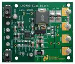
LM3495 Buck Controller Evaluation Module User's Guide
Table of Contents
1 Specifications Of The Board..................................................................................................................................................2
2 Example Circuit.......................................................................................................................................................................2
3 Powering The Converter........................................................................................................................................................ 2
4 Enabling The Converter......................................................................................................................................................... 2
5 Testing The Converter............................................................................................................................................................ 3
6 SKIP/PWM................................................................................................................................................................................3
7 MOSFET Footprints................................................................................................................................................................ 3
8 Permanent Components........................................................................................................................................................ 3
9 Additional Footprints..............................................................................................................................................................4
10 Complete Circuit Schematic................................................................................................................................................ 5
11 Connection Diagrams...........................................................................................................................................................6
12 Typical Performance Waveforms........................................................................................................................................ 7
13 Bill of Materials (BOM)........................................................................................................................................................10
14 PCB Layout..........................................................................................................................................................................11
15 Revision History................................................................................................................................................................. 14
Trademarks
All trademarks are the property of their respective owners.
SNVA149C – MARCH 2006 – REVISED FEBRUARY 2022
LM3495 Buck Controller Evaluation Module User's Guide
Submit Document Feedback
Copyright © 2022 Texas Instruments Incorporated
1
�Specifications Of The Board
www.ti.com
1 Specifications Of The Board
The evaluation board has been designed to test various circuits using the LM3495 buck regulator controller.
Figure 10-1 shows a complete schematic for all components. The board has four layers, consisting of signal/
power traces on the top and bottom, one internal ground plane, and an internal split power plane. The top and
bottom planes are 1-oz. copper, internal planes are 1/2 oz., and the board is 62-mil FR4 laminate.
2 Example Circuit
The example circuit that comes on the evaluation board steps input voltages of 12 V ±10% down to 1.2 V at
currents up to 10 A with a switching frequency of 500 kHz. The measured efficiency of the converter is 86% at
an output current of 7 A.
Figure 2-1. Efficiency for VIN = 12 V
3 Powering The Converter
The example circuit for the LM3495 evaluation board is optimized to run at inputs of 12 V, however the circuit
will operate with input voltages ranging from 2.9 V to 18.0 V connected between the ‘VIN’ and ‘GND’ terminals at
the top of the board. Fixed loads, resistors, and variable electronic loads can be connected between the ‘Vo’ and
‘GND’ terminals. Table 13-1 lists all the components used in the example circuit.
4 Enabling The Converter
The SPDT switch ON/OFF controls the state of the converter while power is applied to the input terminals. While
in the OFF position the COMP/SD* pin of the LM3495 is grounded, the output is disabled, and the IC enters a
low power state. While in the ON position the output voltage is regulated and is capable of delivering current to a
load connected at the output terminals.
2
LM3495 Buck Controller Evaluation Module User's Guide
SNVA149C – MARCH 2006 – REVISED FEBRUARY 2022
Submit Document Feedback
Copyright © 2022 Texas Instruments Incorporated
�www.ti.com
Testing The Converter
5 Testing The Converter
Figure 11-1 shows a block diagram of connections for making measurements of efficiency. The wires used
for making connections at both the input and output should be rated to at least 10 A of continuous current
and should be no longer than is needed for convenient testing. A series ammeter capable of measuring 10
A or more should be used for both the input and the output lines. Dedicated voltmeters should be connected
with their positive and negative leads right at the four power terminals at the top of the evaluation board. This
measurement technique minimizes the voltage loss in the wires that connect the evaluation board to the input
power supply and the electronic load.
Output voltage ripple measurements should be taken directly across the 100-nF ceramic capacitor, Cox, placed
right between the output terminals. Care must be taken to minimize the loop area between the oscilloscope
probe tip and the ground lead. One method to minimize this loop is to remove the spring tip and ‘pigtail’ ground
lead of the probe and then wind bare wire around the probe shaft. The bare wire should contact the ground of
the probe and the end of the wire can then contact the ground side of Cox. Figure 11-2 shows a diagram of this
method.
An oscilloscope probe modified as described above can also be used to measure the switch node voltage, LG
pin voltage, and HG pin voltage (all three with respect to ground) using the 40-mil diameter hole pairs labeled “+
SW –“, “+ LG –“, and “+ HG –“, respectively.
6 SKIP/PWM
A second SPDT switch labeled SKIP/FPWM determines that control scheme the LM3495 uses at low output
currents. When set to SKIP, the converter saves energy during light loads (approximately 100 mA or less) by
using the body diode of the low-side FET, as well as leaving the high-side FET off if possible. When the switch is
set to FPWM, the LM3495 forces both top and bottom FETs to switch during every cycle, regardless of the load
current.
7 MOSFET Footprints
The LM3495 evaluation board has footprints for single N-MOSFETs with SO-8 packages and standard pinouts.
These footprints can also accept newer MOSFET packages that are compatible with SO-8 footprints. See Figure
7-1. Q1 is the high-side FET and Q2 low-side FET.
S
D
S
D
SO-8
S
D
G
D
Figure 7-1. SO-8 MOSFET Pinout
8 Permanent Components
The following components should remain the same for any new circuits evaluated on the LM3495 evaluation
board:
Name
Value
Cb
0.1 µF
Cf
1 µF
Cdd
2.2 µF
SNVA149C – MARCH 2006 – REVISED FEBRUARY 2022
LM3495 Buck Controller Evaluation Module User's Guide
Submit Document Feedback
Copyright © 2022 Texas Instruments Incorporated
3
�Additional Footprints
www.ti.com
9 Additional Footprints
A 100-pF ceramic capacitor should be placed at position Dsync whenever the LM3495 runs without an external
clock. When an external clock is used, Dsync should be removed and a 100-pF ceramic capacitor placed at
Csync.
The 0-Ω resistor J1 connects the TRACK pin and VDD pins of the LM3495 together. It should be removed only
when the tracking function is used.
The 0-Ω resistor J2 connects the VIN and VLIN5 terminals of the LM3495 together. This resistor should be used
only when the input voltage is 5.5 V or less to provide maximum MOSFET gate drive.
The 0-Ω resistor J3 connects the ‘VIN’ terminal to the VIN pin of the LM3495. This resistor should be removed
only for testing of the input current draw of the LM3495 IC.
The 0-Ω resistor Rbst can be replaced with a higher value resistor to limit the current drawn by the BOOST pin.
This slows the high-side FET gate drive rise time and can reduce ringing on the switch node. Care must be
taken, as slowing the gate drive too much can cause shoot-through current.
Components Rt1 and Rt2 are used if the output of the converter is tracking another supply during start-up. For
this application, the output of the external supply should be connected to the TRACK IN terminal. When the
tracking feature is not used, the track pin should be connected to the VDD pin by placing a 0-Ω resistor in
position J2.
Components Rsnb and Csnb can be used to filter ringing on the switch node.
D2 provides a position for a diode to go in parallel with Q2. In circuits with output currents of approximately 5 A
or less, a Schottky diode at D2 can improve the efficiency of the converter.
4
LM3495 Buck Controller Evaluation Module User's Guide
SNVA149C – MARCH 2006 – REVISED FEBRUARY 2022
Submit Document Feedback
Copyright © 2022 Texas Instruments Incorporated
�www.ti.com
Complete Circuit Schematic
10 Complete Circuit Schematic
J3
CDD
CF
VLIN5
1 PF
2.2 PF
D1
J2
LIN
J1
TRACK
IN
RT2
13
9
VIN
TRACK
Vin
14
CB
BOOST
RT1
SYNC
IN
1
VLIN5
RBST
2
8
FREQ/SYNC
+
CIN1
+
CIN2
0.1 PF
Q1
HG
CSYNC
CINX
3
SW/CSH
DSYNC
RFRQ
LM3495
LG
6
SKIP/FPWM
5
L1
RLIM
Vo
ILIM
15
FPWM
4
Q2
+ C
O1
+ C
O2
COX
RSNB
COMP/SD
ON/OFF
CSNB
RLG
CSL
11
D2
16
FB
CC1
CC2
10
SNS
SGND
7
12
PGND
RC1
RFB2
RFB1
Figure 10-1. Circuit Schematic
SNVA149C – MARCH 2006 – REVISED FEBRUARY 2022
LM3495 Buck Controller Evaluation Module User's Guide
Submit Document Feedback
Copyright © 2022 Texas Instruments Incorporated
5
�Connection Diagrams
www.ti.com
11 Connection Diagrams
Ammeter
Ammeter
A
+
50W , 10 A
Electronic Load
A
+
18V , 6A Power
Supply
-
Vo
Voltmeter
GND
GND
Vin
V
V
Voltmeter
LM3495
Evaluation Board
Figure 11-1. Efficiency Measurement Setup
Oscilloscope
Vo
GND
Cox
Figure 11-2. Output Voltage Ripple Measurement Setup
6
LM3495 Buck Controller Evaluation Module User's Guide
SNVA149C – MARCH 2006 – REVISED FEBRUARY 2022
Submit Document Feedback
Copyright © 2022 Texas Instruments Incorporated
�www.ti.com
Typical Performance Waveforms
12 Typical Performance Waveforms
Figure 12-1. Switch Node Voltage (VIN = 12 V, VO = 1.2 V, IO = 5 A)
Figure 12-2. Switch Node Voltage (VIN = 12 V, VO = 1.2 V, IO = 5 A)
SNVA149C – MARCH 2006 – REVISED FEBRUARY 2022
LM3495 Buck Controller Evaluation Module User's Guide
Submit Document Feedback
Copyright © 2022 Texas Instruments Incorporated
7
�Typical Performance Waveforms
www.ti.com
Figure 12-3. Output Voltage Ripple, AC Coupled (VIN = 12 V, VO = 1.2 V, IO = 5 A)
Figure 12-4. Load Transient Response (VIN = 12 V, VO = 1.2 V, IO = 0 A to 4 A)
8
LM3495 Buck Controller Evaluation Module User's Guide
SNVA149C – MARCH 2006 – REVISED FEBRUARY 2022
Submit Document Feedback
Copyright © 2022 Texas Instruments Incorporated
�www.ti.com
Typical Performance Waveforms
Figure 12-5. Load Transient Response (VIN = 12 V, VO = 1.2 V, IO = 4 A to 0 A)
SNVA149C – MARCH 2006 – REVISED FEBRUARY 2022
LM3495 Buck Controller Evaluation Module User's Guide
Submit Document Feedback
Copyright © 2022 Texas Instruments Incorporated
9
�Bill of Materials (BOM)
www.ti.com
13 Bill of Materials (BOM)
Table 13-1. Bill of Materials (BOM)
10
Qty
ID
Part Number
Type
Size
Parameters
Vendor
1
U1
LM3495
Synchronous
Controller
TSSOP-16
1
Q1
HAT2198R
N-MOSFET
SO-8
30 V, 9.6 mΩ
11 nC
Renesas
1
Q2
HAT2165H
N-MOSFET
LFPAK
30 V
3.4 mΩ, 33 nC
Renesas
1
D1
MBR0530
Schottky Diode
SMA
30 V, 0.5 A
Vishay
1
L1
RLF12560T-1R0N140
Inductor
12.5x12.8 x6.0mm
1 µH, 14 A, 3 mΩ
TDK
1
Cin
C3225X5R1E226M
Capacitor
1210
22 µF, 25 V
TDK
2
Co1, Co2
C3225X5R0J107M
Capacitor
1210
100 µF, 6.3 V, 1 mΩ
TDK
1
Cf
C3216X7R1E105M
Capacitor
1206
1 µF, 25 V
TDK
TI
1
Cdd
C3216X7R1E225M
Capacitor
1206
2.2 µF, 25 V
TDK
2
Cb, Cinx
VJ1206Y104KXXAT
Capacitor
1206
100 nF, 10%
Vishay
1
Cc1
VJ1206Y103KXXAT
Capacitor
1206
10 nF, 10%
Vishay
3
Cc2, Csync,
Dsync
VJ1206A101KXXAT
Capacitor
1206
100 pF, 10%
Vishay
1
Cox
VJ0805Y104KXXAT
Capacitor
805
100 nF, 10%
Vishay
3
Rbst, J1, J3
CRCW08050R00F
Resistor
805
0Ω
Vishay
1
Lin
CRCW25120R00F
Resistor
2512
0Ω
Vishay
1
Rc1
CRCW12061501F
Resistor
1206
1.5 kΩ, 1%
Vishay
2
Rfb1, Rfb2
CRCW12061002F
Resistor
1206
10 kΩ, 1%
Vishay
1
Rfrq
CRCW12065492F
Resistor
1206
54.9 kΩ, 1%
Vishay
1
Rlg
CRCW12061R00F
Resistor
1206
1 Ω, 1%
Vishay
1
Rlim
CRCW12063321F
Resistor
1206
3.32 kΩ, 1%
Vishay
2
SKIP/FPWM
ON/OFF
NKK A12AB
SPST
5
Vo, GND1
GND2, GND3
Vin
Newark 40F6004
Terminal Silver
0.094”
Cambion
4
SYNC IN
GND4, GND5
TRACK IN
Newark 94F1478
Terminal Silver
0.062”
Keystone
LM3495 Buck Controller Evaluation Module User's Guide
NKK
SNVA149C – MARCH 2006 – REVISED FEBRUARY 2022
Submit Document Feedback
Copyright © 2022 Texas Instruments Incorporated
�www.ti.com
PCB Layout
14 PCB Layout
Figure 14-1. Top Layer and Top Overlay
SNVA149C – MARCH 2006 – REVISED FEBRUARY 2022
LM3495 Buck Controller Evaluation Module User's Guide
Submit Document Feedback
Copyright © 2022 Texas Instruments Incorporated
11
�PCB Layout
www.ti.com
Figure 14-2. Bottom Layer
12
LM3495 Buck Controller Evaluation Module User's Guide
SNVA149C – MARCH 2006 – REVISED FEBRUARY 2022
Submit Document Feedback
Copyright © 2022 Texas Instruments Incorporated
�www.ti.com
PCB Layout
Figure 14-3. Internal Layer 1
SNVA149C – MARCH 2006 – REVISED FEBRUARY 2022
LM3495 Buck Controller Evaluation Module User's Guide
Submit Document Feedback
Copyright © 2022 Texas Instruments Incorporated
13
�Revision History
www.ti.com
Figure 14-4. Internal Layer 2
15 Revision History
NOTE: Page numbers for previous revisions may differ from page numbers in the current version.
Changes from Revision B (April 2013) to Revision C (February 2022)
Page
• Updated the numbering format for tables, figures, and cross-references throughout the document. ................2
• Updated the user's guide title............................................................................................................................. 2
14
LM3495 Buck Controller Evaluation Module User's Guide
SNVA149C – MARCH 2006 – REVISED FEBRUARY 2022
Submit Document Feedback
Copyright © 2022 Texas Instruments Incorporated
�IMPORTANT NOTICE AND DISCLAIMER
TI PROVIDES TECHNICAL AND RELIABILITY DATA (INCLUDING DATA SHEETS), DESIGN RESOURCES (INCLUDING REFERENCE
DESIGNS), APPLICATION OR OTHER DESIGN ADVICE, WEB TOOLS, SAFETY INFORMATION, AND OTHER RESOURCES “AS IS”
AND WITH ALL FAULTS, AND DISCLAIMS ALL WARRANTIES, EXPRESS AND IMPLIED, INCLUDING WITHOUT LIMITATION ANY
IMPLIED WARRANTIES OF MERCHANTABILITY, FITNESS FOR A PARTICULAR PURPOSE OR NON-INFRINGEMENT OF THIRD
PARTY INTELLECTUAL PROPERTY RIGHTS.
These resources are intended for skilled developers designing with TI products. You are solely responsible for (1) selecting the appropriate
TI products for your application, (2) designing, validating and testing your application, and (3) ensuring your application meets applicable
standards, and any other safety, security, regulatory or other requirements.
These resources are subject to change without notice. TI grants you permission to use these resources only for development of an
application that uses the TI products described in the resource. Other reproduction and display of these resources is prohibited. No license
is granted to any other TI intellectual property right or to any third party intellectual property right. TI disclaims responsibility for, and you
will fully indemnify TI and its representatives against, any claims, damages, costs, losses, and liabilities arising out of your use of these
resources.
TI’s products are provided subject to TI’s Terms of Sale or other applicable terms available either on ti.com or provided in conjunction with
such TI products. TI’s provision of these resources does not expand or otherwise alter TI’s applicable warranties or warranty disclaimers for
TI products.
TI objects to and rejects any additional or different terms you may have proposed. IMPORTANT NOTICE
Mailing Address: Texas Instruments, Post Office Box 655303, Dallas, Texas 75265
Copyright © 2022, Texas Instruments Incorporated
�


 工商网监
湘ICP备2023018690号
工商网监
湘ICP备2023018690号
