Product
Folder
Sample &
Buy
Support &
Community
Tools &
Software
Technical
Documents
LM3532
SNVS653E – JULY 2011 – REVISED AUGUST 2015
LM3532 High-Efficiency White LED Driver With Programmable Ambient Light Sensing
Capability and I2C-Compatible Interface
1 Features
3 Description
•
The LM3532 is a 500-kHz fixed frequency
asynchronous boost converter which provides the
power for 3 high-voltage, low-side current sinks. The
device is programmable over an I2C-compatible
interface and has independent current control for all
three channels. The adaptive current regulation
method allows for different LED currents in each
current sink thus allowing for a wide variety of
backlight and keypad applications.
1
•
•
•
•
•
•
•
•
•
•
Drives up to 3 Parallel High-Voltage LED Strings
at 40 V Each With up to 90% Efficiency
0.4% Typical Current Matching Between Strings
256 Level Logarithmic and Linear Brightness
Control With 14-Bit Equivalent Dimming
I2C-Compatible Interface
Direct Read Back of Ambient Light Sensor Via
8-bit ADC
Programmable Dual Ambient Light Sensor Inputs
With Internal Sensor Gain Selection
Dual External PWM Inputs for LED Brightness
Adjustment
Independent Current String Brightness Control
Programmable LED Current Ramp Rates
40-V Overvoltage Protection
1-A Typical Current Limit
The main features of the LM3532 include dual
ambient light sensor inputs each with 32 internal
voltage setting resistors, 8-bit logarithmic and linear
brightness control, dual external PWM brightness
control inputs, and up to 1000:1 dimming ratio with
programmable fade in and fade out settings.
The LM3532 is available in a 16-pin, 0.4-mm pitch
thin DSBGA package. The device operates over a
2.7-V to 5.5-V input voltage range and the −40°C to
+85°C temperature range.
2 Applications
•
•
Device Information(1)
Power Source for White LED Backlit LCD Displays
Programmable Keypad Backlight
PART NUMBER
LM3532
PACKAGE
DSBGA (16)
BODY SIZE (MAX)
1.87 mm x 1.77 mm
(1) For all available packages, see the orderable addendum at
the end of the data sheet.
Typical Application Circuit
L
VOUT up to 40V
D1
VIN
CIN
COUT
IN
SW
OVP
VALS
Ambient Light
Sensor 1
VIN
Ambient Light
Sensor 2
ALS1
ALS2
LM3532
SDA
SCL
INT
ILED1
ILED2
ILED3
PWM1
T0
PWM2
HWEN
PGND
1
An IMPORTANT NOTICE at the end of this data sheet addresses availability, warranty, changes, use in safety-critical applications,
intellectual property matters and other important disclaimers. PRODUCTION DATA.
�LM3532
SNVS653E – JULY 2011 – REVISED AUGUST 2015
www.ti.com
Table of Contents
1
2
3
4
5
6
7
Features ..................................................................
Applications ...........................................................
Description .............................................................
Revision History.....................................................
Pin Configuration and Functions .........................
Specifications.........................................................
1
1
1
2
3
4
6.1
6.2
6.3
6.4
6.5
6.6
6.7
6.8
4
4
4
4
5
6
6
7
Absolute Maximum Ratings ......................................
ESD Ratings..............................................................
Recommended Operating Conditions.......................
Thermal Information ..................................................
Electrical Characteristics...........................................
I2C-Compatible Timing Specifications (SCL, SDA)...
Switching Characteristics ..........................................
Typical Characteristics ..............................................
Detailed Description .............................................. 9
7.1 Overview ................................................................... 9
7.2 Functional Block Diagram ......................................... 9
7.3 Feature Description................................................... 9
7.4 Device Functional Modes........................................ 12
7.5 Programming........................................................... 23
7.6 Register Maps ......................................................... 24
8
Application and Implementation ........................ 34
8.1 Application Information............................................ 34
8.2 Typical Application ................................................. 34
9 Power Supply Recommendations...................... 41
10 Layout................................................................... 42
10.1 Layout Guidelines ................................................. 42
10.2 Layout Examples................................................... 45
11 Device and Documentation Support ................. 47
11.1
11.2
11.3
11.4
11.5
11.6
Device Support......................................................
Documentation Support .......................................
Community Resources..........................................
Trademarks ...........................................................
Electrostatic Discharge Caution ............................
Glossary ................................................................
47
47
47
47
47
47
12 Mechanical, Packaging, and Orderable
Information ........................................................... 47
4 Revision History
NOTE: Page numbers for previous revisions may differ from page numbers in the current version.
Changes from Revision D (June 2013) to Revision E
•
Added Device Information and Pin Configuration and Functions sections, ESD Ratings table, Feature Description,
Device Functional Modes, Application and Implementation, Power Supply Recommendations, Layout, Device and
Documentation Support, and Mechanical, Packaging, and Orderable Information sections ................................................. 1
Changes from Revision C (March 2013) to Revision D
•
Page
Page
Updated Output Configuration Register defaults: in col. 2 from "00" to "1X"; in col. 3 from "00" to "01"............................. 25
Changes from Revision B (July 2012) to Revision C
Page
•
added "IFULL_SCALE = 20.2mA, Brightness Code = 0xFF" to 2.7V ≤ VIN ≤ 5.5V in conditions for Imatch ................................. 5
•
Changed layout of National Data Sheet to TI format ........................................................................................................... 46
2
Submit Documentation Feedback
Copyright © 2011–2015, Texas Instruments Incorporated
Product Folder Links: LM3532
�LM3532
www.ti.com
SNVS653E – JULY 2011 – REVISED AUGUST 2015
5 Pin Configuration and Functions
YFQ Package
16-Pin DSBGA
Top View
A1
A2
A3
A4
B1
B2
B3
B4
C1
C2
C3
C4
D1
D2
D3
D4
Pin Functions
PIN
TYPE
DESCRIPTION
NO.
NAME
A1
OVP
IN
Output voltage sense connection for overvoltage sensing. Connect OVP to the positive terminal of the
output capacitor.
A2
ILED3
IN
Input terminal to high voltage current sink 3 (40 V maximum). The boost converter regulates the
minimum of ILED1, ILED2, or ILED3 to 0.4V.
A3
ILED2
IN
Input terminal to high voltage current sink 2 (40 V maximum). The boost converter regulates the
minimum of ILED1, ILED2, or ILED3 to 0.4V.
A4
ILED1
IN
Input terminal to high voltage current sink 1 (40 V maximum). The boost converter regulates the
minimum of ILED1, ILED2, or ILED3 to 0.4V.
B1
ALS1
IN
Ambient light sensor input 1.
B2
ALS2
IN
Ambient light sensor input 2.
B3
HWEN
IN
Active high hardware enable. Pull this pin high to enable the LM3532. HWEN is a high impedance input.
B4
IN
IN
Input voltage connection. Bypass IN to GND with a minimum 2.2-µF ceramic capacitor.
C1
PWM2
IN
External PWM brightness control Input 2.
C2
PWM1
IN
External PWM brightness Ccontrol Input 1.
C3
INT
OUT
Programmable Interrupt pin. INT is an open-drain output that pulls low when the ALS changes zones.
C4
GND
GND
Ground
D1
SDA
I/O
Serial data connection for I2C-compatible interface
D2
SCL
IN
Serial clock connection for I2C-compatible interface
D3
TO
IN
Unused test input. This pin must be tied externally to GND for proper operation.
D4
SW
IN
Drain connection for boost converters internal NFET
Submit Documentation Feedback
Copyright © 2011–2015, Texas Instruments Incorporated
Product Folder Links: LM3532
3
�LM3532
SNVS653E – JULY 2011 – REVISED AUGUST 2015
www.ti.com
6 Specifications
6.1 Absolute Maximum Ratings
over operating free-air temperature range (unless otherwise noted) (1) (2) (3)
MIN
MAX
UNIT
VIN to GND
V
VSW, VOVP, VILED1, VILED2, VILED3 to GND
V
VSCL, VSDA, VALS1, VALS2, VPWM1, VPWM2, VINT,
VHWEN, VT0 to GND
V
Continuous power dissipation
Internally Limited
Junction temperature , TJ-MAX
150
°C
Maximum lead temperature (soldering, 10s) (4)
300
°C
150
°C
−65
Storage temperature, Tstg
(1)
(2)
(3)
(4)
Stresses beyond those listed under Absolute Maximum Ratings may cause permanent damage to the device. These are stress ratings
only, which do not imply functional operation of the device at these or any other conditions beyond those indicated under Recommended
Operating Conditions. Exposure to absolute-maximum-rated conditions for extended periods may affect device reliability.
If Military/Aerospace specified devices are required, contact the Texas Instruments Sales Office/ Distributors for availability and
specifications
All voltages are with respect to the potential at the GND pin.
For detailed soldering specifications and information, refer to Application Note AN-1112: DSBGA Wafer Level Chip Scale Package
(SNVA009).
6.2 ESD Ratings
VALUE
V(ESD)
(1)
(2)
Electrostatic
discharge
Human-body model (HBM), per ANSI/ESDA/JEDEC JS-001
(1)
±2000
Charged-device model (CDM), per JEDEC specification JESD22-C101 (2)
UNIT
V
±5000
JEDEC document JEP155 states that 500-V HBM allows safe manufacturing with a standard ESD control process.
JEDEC document JEP157 states that 250-V CDM allows safe manufacturing with a standard ESD control process.
6.3 Recommended Operating Conditions
over operating free-air temperature range (unless otherwise noted) (1) (2)
MIN
VIN to GND
VSW, VOVP, VILED1, VILED2, VILED3 to GND
Junction temperature, TJ (3) (4)
(1)
(2)
(3)
(4)
NOM
MAX
2.7
5.5
UNIT
V
0
40
V
–40
125
°C
Stresses beyond those listed under Absolute Maximum Ratings may cause permanent damage to the device. These are stress ratings
only, which do not imply functional operation of the device at these or any other conditions beyond those indicated under Recommended
Operating Conditions. Exposure to absolute-maximum-rated conditions for extended periods may affect device reliability.
All voltages are with respect to the potential at the GND pin.
Internal thermal shutdown circuitry protects the device from permanent damage. Thermal shutdown engages at TJ= 140°C (typical) and
disengages at TJ= 125°C (typical).
In applications where high power dissipation and/or poor package thermal resistance is present, the maximum ambient temperature may
have to be derated. Maximum ambient temperature (TA-MAX) is dependent on the maximum operating junction temperature (TJ-MAX-OP =
125°C), the maximum power dissipation of the device in the application (PD-MAX), and the junction-to ambient thermal resistance of the
part/package in the application (RθJA), as given by the following equation: TA-MAX = TJ-MAX-OP – (RθJA × PD-MAX).
6.4 Thermal Information
LM3532
THERMAL METRIC
(1)
YFQ (DSBGA)
UNIT
16 PINS
RθJA
(1)
4
Junction-to-ambient thermal resistance
61.3
°C/W
For more information about traditional and new thermal metrics, see the Semiconductor and IC Package Thermal Metrics application
report, SPRA953.
Submit Documentation Feedback
Copyright © 2011–2015, Texas Instruments Incorporated
Product Folder Links: LM3532
�LM3532
www.ti.com
SNVS653E – JULY 2011 – REVISED AUGUST 2015
6.5 Electrical Characteristics
Minimum and maximum limits apply over the full operating ambient temperature range (−40°C ≤ TA ≤ +85°C), typical limits are
for TA = 25°C, and VIN = 3.6 V, unless otherwise specified. (1) (2)
PARAMETER
ILED(1/2/3)
IMATCH
(3) (4)
TEST CONDITIONS
2.7 V ≤ VIN ≤ 5.5 V, ControlX full-scale
current register = 0xF3, brightness code =
Output current regulation accuracy 0xFF
(ILED1, ILED2 or ILED3)
2.7 V ≤ VIN ≤ 5.5 V, ControlX full-scale
current register = 0xF3, brightness code =
0xFF
ILED2 to ILED3 current matching
MIN
MAX
20.2
18.68
2.7 V ≤ VIN ≤ 5.5 V, IFULL_SCALE = 20.2 mA
Brightness code = 0xFF
2.7 V ≤ VIN ≤ 5.5 V, IFULL_SCALE = 20.2 mA
Brightness code = 0xFF
TYP
UNIT
mA
21.8
mA
0.3%
–2%
2%
VREG_CS
Regulated current sink headroom
voltage
VHR
Current sink minimum headroom
voltage
ILED = 95% of nominal and 20.2 mA
RDSON
NMOS switch on resistance
ISW = 100 mA
0.25
Ω
2.7 V ≤ VIN ≤ 5.5 V
1000
mA
ICL
NMOS switch current limit
400
200
ILED = 95% of nominal and 20.2 mA
2.7 V ≤ VIN ≤ 5.5 V
mV
240
880
ON threshold, 2.7 V ≤ VIN ≤ 5.5 V
ON threshold, 2.7 V ≤ VIN ≤ 5.5 V
mV
1000
1120
mA
41
VOVP
Output overvoltage protection
DMAX
Maximum duty cycle
94%
DMIN
Minimum duty cycle
10%
IQ
Quiescent current into IN, device
not switching
ILED1 = ILED2 = ILED3 = 20.2 mA,
feedback disabled
490
µA
IQ_SW
Switching supply current
ILED1 = ILED2 = ILED3 = 20.2 mA, VOUT = 32
V
1.35
mA
ISHDN
Shutdown current
ILED_MIN
Minimum LED Current in ILED1,
ILED2 or ILED3
Hysteresis
2.7 V ≤ VIN ≤ 5.5 V, HWEN = GND
TSD
(1)
(2)
(3)
(4)
40
42
1
1
2.7 V ≤ VIN ≤ 5.5 V, HWEN = GND
−40°C ≤ TA ≤ +85°C
Full-scale current =20.2 mA
Brightness code = 0x01, Mapping =
Exponential
Thermal Shutdown
2
9.5
140
Hysteresis
V
15
µA
µA
°C
All voltages are with respect to the potential at the GND pin.
Minimum and Maximum limits are verified by design, test, or statistical analysis. Typical numbers are not verified, but do represent the
most likely norm.
All current sinks for the matching spec are assigned to the same control bank.
LED current sink matching between ILED2 and ILED3 is given by taking the difference between either (ILED2 or ILED3) and the
average current between the two, and dividing by the average current between the two (ILED2/3 – ILED(AVE))/ILED(AVE). This
simplifies to (ILED2 – ILED3)/(ILED2 + ILED3). In this test, both ILED2 and ILED3 are assigned to Bank A.
Submit Documentation Feedback
Copyright © 2011–2015, Texas Instruments Incorporated
Product Folder Links: LM3532
5
�LM3532
SNVS653E – JULY 2011 – REVISED AUGUST 2015
www.ti.com
Electrical Characteristics (continued)
Minimum and maximum limits apply over the full operating ambient temperature range (−40°C ≤ TA ≤ +85°C), typical limits are
for TA = 25°C, and VIN = 3.6 V, unless otherwise specified.(1)(2)
PARAMETER
TEST CONDITIONS
MIN
TYP
MAX
UNIT
LOGIC INPUTS/OUTPUTS (PWM1, PWM2, HWEN, SCL, SDA, INT)
VIL
Input logic low
2.7 V ≤ VIN ≤ 5.5 V
0
0.4
VIH
Input logic high
2.7 V ≤ VIN ≤ 5.5 V
1.2
VIN
VOL
Output logic low (SCL, INT)
2.7 V ≤ VIN ≤ 5.5 V, ILOAD = 3 mA
RPWM
PWM input internal pulldown
resistance (PWM1, PWM2)
0.4
100
V
V
kΩ
AMBIENT LIGHT SENSOR INPUTS (ALS1, ALS2)
ALS1, ALS2 Resistor Select
Register = 0x0F, 2.7 V ≤ VIN ≤ 5.5 V
RALS1,
RALS2
ALS pin internal pulldown resistors
VALS_REF
Ambient light sensor reference
voltage
2.7 V ≤ VIN ≤ 5.5 V
VOS
ALS input offset voltage
(Code 0-to-1 transition – VLSB)
2.7 V ≤ VIN ≤ 5.5 V
tCONV
Conversion time
LSB
ADC resolution
2.44
kΩ
ALS1, ALS2 Resistor Select
Register = 0x0F, 2.7 V ≤ VIN ≤ 5.5 V
2.29
2.59
2
2.7 V ≤ VIN ≤ 5.5 V
1.94
2.06
2.5
2.7 V ≤ VIN ≤ 5.5 V
0.8
4.2
154
2.7V ≤ VIN ≤ 5.5V
7.84
V
mV
µs
mV
6.6 I2C-Compatible Timing Specifications (SCL, SDA)
See (1)
MIN
NOM
MAX
UNIT
t1
SCL (clock period)
2.5
µs
t2
Data In setup time to SCL high
100
ns
t3
Data out stable after SCL low
0
ns
t4
SDA low setup time to SCL low (start)
100
ns
t5
SDA high hold time after SCL high (stop)
100
ns
(1)
SCL and SDA must be glitch-free in order for proper brightness control to be realized.
6.7 Switching Characteristics
over operating free-air temperature range (unless otherwise noted)
PARAMETER
TEST CONDITIONS
MIN
2.7 V ≤ VIN ≤ 5.5 V
ƒSW
6
Switching frequency
2.7 V ≤ VIN ≤ 5.5 V
−40°C ≤ TA ≤ 85°C
Submit Documentation Feedback
TYP
MAX
UNIT
500
450
550
kHz
Copyright © 2011–2015, Texas Instruments Incorporated
Product Folder Links: LM3532
�LM3532
www.ti.com
SNVS653E – JULY 2011 – REVISED AUGUST 2015
6.8 Typical Characteristics
VIN = 3.6 V, LEDs (VF = 3.2 V at 20 mA, TA = 25°C), COUT = 1 µF, CIN = 2.2 µF, TA = 25°C unless otherwise specified.
240.0
1.6
220.0
-40°C
200.0
85C
1.2
'ILED (PA)
Shutdown Current (PA)
1.4
-40C
25C
0.9
0.7
180.0
240.0
220.0
160.0
200.0
180.0
160.0
140.0
140.0
120.0
120.0
100.0
80.0
60.0
100.0
40.0
20.0
80.0
0.0
60.0
25°C
40.0
85°C
20.0
0.5
2.5
0.0
3.1
3.7
4.3
4.9
2.5
3.1
3.7
5.5
4.3
4.9
5.5
VIN (V)
VIN (V)
HWEN = GND
Figure 1. Shutdown Current vs VIN
Figure 2. Current Sink Matching vs VIN ILED2 To ILED3
500
450
TA = -40°C
2.450k
400
2.448k
300
RALS1 (:)
'ILED (PA)
350
TA = +85°C
250
200
2.446k
85°C
2.444k
2.442k
25°C
2.440k
2.438k
150
2.436k
TA = +25°C
100
50
2.5
-40°C
3.1
3.7
4.3
4.9
5.5
2.5
3.0
3.5
(ΔILED is worst case difference between all three strings)
4.5
5.0
5.5
2.44-kΩ Setting
Figure 4. ALS Resistance vs VIN RALS1
Figure 3. Current Sink Matching vs VIN ILED1 to ILED2 To
ILED3
10.000
1.00
8.000
0.75
6.000
0.50
4.000
85°C
0.25
2.000
LSB's
ALS Resistor Matching (:)
4.0
VIN (V)
VIN (V)
0.000
25°C
-2.000
0.00
-0.25
-4.000
-0.50
-6.000
-40°C
-8.000
-10.000
2.5
3.0
3.5
4.0
-0.75
4.5
5.0
-1.00
0
5.5
32
64
96
128 160 192 224 256
VIN (V)
Code (D)
Figure 5. Als Resistor Matching vs VIN
Figure 6. Integral Non Linearity vs Code (Endpoint Method)
2.44-kΩ Setting
Submit Documentation Feedback
Copyright © 2011–2015, Texas Instruments Incorporated
Product Folder Links: LM3532
7
�LM3532
SNVS653E – JULY 2011 – REVISED AUGUST 2015
www.ti.com
Typical Characteristics (continued)
VIN = 3.6 V, LEDs (VF = 3.2 V at 20 mA, TA = 25°C), COUT = 1 µF, CIN = 2.2 µF, TA = 25°C unless otherwise specified.
1.00
22.0
0.90
20.0
0.80
LED Current Ripple (mA)
18.0
0.70
LSB's
0.60
0.50
0.40
0.30
0.20
16.0
14.0
12.0
10.0
8.0
6.0
0.10
4.0
0.00
2.0
-0.10
0
32
64
96
0.0
0.01
128 160 192 224 256
0.1
1
10
100
fPWM (kHz)
Code (D)
Figure 8. Peak-to-Peak LED Current Ripple vs FPWM
Figure 7. Differential Non Linearity vs Code
31
30
29
-40°C
28
ILED (mA)
27
26
25°C
25
85°C
24
23
22
21
20
19
0.10
0.15
0.20
0.25
0.30
0.35
0.40
VHR (V)
Figure 9. LED Current vs Headroom Voltage
8
Submit Documentation Feedback
Copyright © 2011–2015, Texas Instruments Incorporated
Product Folder Links: LM3532
�LM3532
www.ti.com
SNVS653E – JULY 2011 – REVISED AUGUST 2015
7 Detailed Description
7.1 Overview
The LM3532 backlight driver consists of three 30-mA current sinks, a dual input ambient light sensor interface,
and a dual input PWM control. The LED current can be controlled via either the I2C bus, the PWM input, the
ambient light sensor interface, or a combination of each. The programmable options via I2C allow for the three
current sinks to be controlled independently or be controlled by a single source.
7.2 Functional Block Diagram
IN
HWEN
Reference, Logic,
Oscillator
OVP
Power
On Reset
(1.8 V)
SW
Overvoltage
Protection (40 V)
Thermal Shutdown
(140°C)
Boost Converter
(0.25-Ÿ NMOS)
1-A Current Limit
500-kHz Switching
Frequency
PWM1
PWM2
Internal Low Pass
Filter
Output Configuration
1. I2C Control
2. I2C x PWM Control
3. PWM Only Control
4. ALS Control
Internal Low Pass
Filter
ALS2
High Voltage Current
Sinks
LED1
LED2
INT
ALS1
400-mV
Headroom
Voltage
LED3
Programmable Input
128 Internal gain
setting resistors
LED Current Ramping
8 µs/step
1 ms/step
2 ms/step
4 ms/step
8 ms/step
16 ms/step
33 ms/step
66 ms/step
ALS Processing
1. 8-bit ADC
2. Averaging
Backlight LED Control
1. 5-bit Full Scale
Current Select
3. ALS Algorithms
2. 8-bit brightness
adjustment
SDA
SCL
3. Linear/Exponential
Dimming
I2C Interface
GND
7.3 Feature Description
7.3.1 40-V Boost Converter
The LM3532 contains a 40-V maximum output voltage, asynchronous boost converter with an integrated 250-mΩ
switch, and three low-side current sinks. Each low-side current sink is independently programmable from 0 to 30
mA.
Submit Documentation Feedback
Copyright © 2011–2015, Texas Instruments Incorporated
Product Folder Links: LM3532
9
�LM3532
SNVS653E – JULY 2011 – REVISED AUGUST 2015
www.ti.com
Feature Description (continued)
7.3.2 Hardware Enable Input
HWEN is the LM3532 device's global hardware enable input. This pin must be driven high to enable the device.
HWEN is a high-impedance input so cannot be left floating. Typically HWEN would be connected through a
pullup resistor to the logic supply voltage or driven high from a microcontroller. Driving HWEN low places the
LM3532 into a low-current shutdown state and force all the internal registers to their power-on reset (POR)
states.
7.3.3 Feedback Enable
Each current sink can be set for feedback enable or feedback disable. When feedback is enabled, the boost
converter maintains at least 400 mV across each active current sink. This causes the boost output voltage (VOUT)
to raise up or down depending on how many LEDs are placed in series in the highest voltage string. This
ensures there is a minimum headroom voltage across each current sink. The potential drawback is that for large
differentials in LED counts between strings, the LED voltage can be drastically different causing the excess
voltage in the lower LED string to be dropped across its current sink. In situations where there are other voltage
sources available, or where the LED count is low enough to use VIN as the power source, the feedback can be
disabled on the specific current sink. This allows for the current sink to be active, but eliminates its control over
the boost output voltage (see Figure 10). In this situation care must be taken to ensure there is always at least
400 mV of headroom voltage across each active current sink to avoid the current from going out of regulation.
Control over the feedback enable/disable is programmable via the Feedback Enable Register (see Table 13).
VIN
SW
OVP
Error Amplifier
400 mV
+
IN
CIN
Boost
Controller
COUT
250 m:
ILED1
ILED2
VHR Min
ILED3
Feedback
Enable
GND
Figure 10. LM3532 Feedback Enable/Disable
7.3.4 LM3532 Current Sink Configuration
Control of the LM3532 device’s three current sinks is done by configuring the three internal control banks
(Control A, Control B, and Control C) (see Figure 11). Any of the current sinks (ILED1, ILED2, or ILED3) can be
mapped to any of the three control banks. Configuration of the control banks is done via the Output Configuration
register.
10
Submit Documentation Feedback
Copyright © 2011–2015, Texas Instruments Incorporated
Product Folder Links: LM3532
�LM3532
www.ti.com
SNVS653E – JULY 2011 – REVISED AUGUST 2015
Feature Description (continued)
Environmental
Stimulus
ALS
Processor
Controls
Outputs
(Masters: Output configuration)
(Ramp rates, brightness management)
(ALS processor select, enable)
(Slaves)
ALS1
ALSP_1
Bank_A
ILED1
PWM
Filters
Bank_B
ILED2
Bank_C
ILED3
ALS2
CABC1
CABC2
PWM_0
PWM_1
Figure 11. LM3532 Functional Control Diagram
7.3.5 PWM Inputs
The LM3532 provides two PWM inputs (PWM1 and PWM2) which can be mapped to any of the three Control
Banks. PWM input mapping is done through the Control A PWM Configuration register, the Control B PWM
Configuration register, and the Control C PWM Configuration register.
Both PWM inputs (PWM1 and PWM2) feed into internal level shifters and lowpass filters. This allows the PWM
inputs to accept logic level signals and convert them to analog control signals which can control the assigned
Control Banks LED current. The internal lowpass filter at each PWM input has a typical corner frequency of 540
Hz with a Q of 0.5. This gives a low end useful PWM frequency of around 2 kHz. Frequencies lower than this
cause the LED current to show larger ripple and result in non-linear behavior vs. duty cycle due to the response
time of the boost circuit. The upper boundary of the PWM frequency is greater than 100 kHz. Frequencies above
200 kHz begin to show non linear behavior due to propagation delays through the PWM input circuitry.
7.3.6 Full-Scale LED Current
There are 32 programmable full-scale current settings for each of the three control banks (Control A, Control B,
and Control C). Each control bank has its own independent full-scale current setting (ILED_FULL_SCALE). Full-scale
current for the respective Control Bank is set via the Control A Full-Scale Current Register, the Control B FullScale Current Register, and the Control C Full-Scale Current Register (see Table 12).
Submit Documentation Feedback
Copyright © 2011–2015, Texas Instruments Incorporated
Product Folder Links: LM3532
11
�LM3532
SNVS653E – JULY 2011 – REVISED AUGUST 2015
www.ti.com
Feature Description (continued)
7.3.7 Interrupt Output
INT is an open drain output that pulls low when the ALS is enabled and when one of the ALS inputs transitions
into a new zone. At the same time, the ALS Zone Information register is updated with the current ALS zone, and
the software flag (bit 3 of the ALS Zone Information register) is written high. A readback of the Zone Information
Register clears the software interrupt flag and reset the INT output to the open drain state. The active pulldown
at INT is typically 125 Ω.
7.3.8 Protection Features
7.3.8.1 Overvoltage Protection
The LM3532 devices’s boost converter provides open-load protection, by monitoring the OVP pin. The OVP pin
is designed to connect as close as possible to the positive terminal of the output capacitor. In the event of a
disconnected load (LED current string with feedback enabled), the output voltage rises in order to try and
maintain the correct headroom across the feedback enabled current sinks (see Table 13). Once VOUT climbs to
the OVP threshold (VOVP) the boost converter is turned off, and switching stops until VOUT falls below the OVP
hysteresis (VOVP – 1 V). Once the OVP hysteresis is crossed the LM3532 device’s boost converter begins
switching again. In open load conditions this would result in a pulsed on/off operation.
7.3.8.2 Current Limit
The LM3532 device’s peak current limit in the NFET is set at typically 1 A (880 mA, minimum). During the
positive portion of the switching cycle, if the NFET's current rises up to the current limit threshold, the NFET turns
off for the rest of the switching cycle. At the start of the next switching cycle the NFET turns on again. For loads
that cause the LM3532 to hit current limit each switching cycle, the output power can become clamped because
the headroom across the feedback enabled current sinks is no longer being regulated when the device is in
current limit. See Maximum Output Power below for guidelines on how peak current affects the LM3532 device's
maximum output power.
7.4 Device Functional Modes
7.4.1 LED Current Ramping
The LM3532 provides 4 methods to control the rate of rise or fall of the LED current during these events:
1. Start-up from 0 to the initial target
2. Shutdown
3. Ramp up from one brightness level to the next
4. Ramp down from one brightness level to the next
See Table 4 and Table 5.
7.4.2 Start-up and Shutdown Current Ramping
The start-up and shutdown ramp rates are independently programmable in the Start-up/Shutdown Ramp Rate
register (see Table 4). There are 8 different start-up and 8 different shutdown ramp rates. The start-up ramp
rates are independently programmable from the shutdown ramp rates, but not independently programmable for
each Control Bank. For example, programming a start-up or shutdown ramp rate, programs the same ramp rate
for each Control Bank.
7.4.3 Run-Time Ramp Rates
Current ramping from one brightness level to the next is programmed via the Run-Time Ramp Rate Register (see
Table 5). There are 8 different ramp-up and 8 different ramp-down rates. The ramp-up rate is independently
programmable from the ramp-down rate, but not independently programmable for each Control Bank. For
example, programming a ramp-up or a ramp-down rate programs the same rate for each Control Bank.
12
Submit Documentation Feedback
Copyright © 2011–2015, Texas Instruments Incorporated
Product Folder Links: LM3532
�LM3532
www.ti.com
SNVS653E – JULY 2011 – REVISED AUGUST 2015
Device Functional Modes (continued)
7.4.4 LED Current Mapping Modes
All LED current brightness codes are 8 bits (256 different levels), where each bit represents a percentage of the
programmed full-scale current setting for that particular Control Bank. The percentage of the full-scale current is
different depending on which mapping mode is selected. The mapping mode can be either exponential or linear.
Mapping mode is selected via bit [1] of the Control A, B, or C Brightness Configuration Registers.
7.4.5 Exponential Current Mapping Mode
In exponential mapping mode, the backlight code to LED current approximates the following equation:
ILED
ILED _ FULLSCALE
ª
« 40
«
u 0.85¬
§ Code
¨¨
© 6.4
1 ·º
¸¸ »
¹ »¼
u DPWM
where
•
•
Code is the 8-bit code in the programmed brightness register
DPWM is the duty cycle of the PWM input that is assigned to the particular control bank
(1)
Figure 12 shows the typical response of percentage of full-scale current setting vs 8-bit brightness code.
% FULL SCALE
100
10
1
0.1
0
16 32 48 64 80 96 112 128 144 160 176 192 208 224 240 256
BRIGHTNESS CODE (D)
Figure 12. Exponential Mapping Response
7.4.6 Linear Current Mapping
In linear mapping mode the backlight code to LED current approximates Equation 2:
ILED = ILED_ FULLSCALE x
1
x Code x DPWM
255
where
•
•
Code is the 8-bit code in the programmed brightness register
DPWM is the duty cycle of the PWM input that is assigned to the particular control bank.
(2)
For the linear mapped mode (Figure 13) shows the typical response of percentage of full-scale current setting vs
8-bit brightness code.
Submit Documentation Feedback
Copyright © 2011–2015, Texas Instruments Incorporated
Product Folder Links: LM3532
13
�LM3532
SNVS653E – JULY 2011 – REVISED AUGUST 2015
www.ti.com
Device Functional Modes (continued)
100
90
% FULL SCALE
80
70
60
50
40
30
20
10
0
0
16 32 48 64 80 96 112 128 144 160 176 192 208 224 240 256
BRIGHTNESS CODE (D)
Figure 13. Linear Mapping Response
7.4.7 LED Current Control
Once the full-scale current is set, control of the LM3532 device’s LED current can be done via 2 methods:
1. I2C Current Control
2. Ambient Light Sensor Current Control
I2C current control allows for the direct control of the LED current by writing directly to the specific brightness
register. In ambient light sensor current control the LED current is automatically set by the ambient light sensor
interface.
7.4.7.1 I2C Current Control
I2C current control is accomplished by using one of the Zone Target Registers (for the respective Control Bank)
as the brightness register. This is done via bits[4:2] of the Control (A, B, or C) Brightness Registers (see Table 9,
Table 10, and Table 11). For example, programming bits[4:2] of the Control A Brightness Register with (000)
makes the brightness register for Bank A (in I2C Current Control) the Control A Zone Target 0 Register.
7.4.7.2 I2C Current Control With PWM
I2C current control can also incorporate the PWM duty cycle at one of the PWM inputs (PWM1 or PWM2). In this
situation the LED current is then a function of both the code in the programmed brightness register and the duty
cycle input into the assigned PWM inputs (PWM1 or PWM2).
7.4.8 Assigning and Enabling a PWM Input
To make the backlight current a function of the PWM input duty cycle, one of the PWM inputs must first be
assigned to a particular Control Bank. This is done via bit [0] of the Control A, B, or C PWM Registers (see
Table 6, Table 7, or Table 8). After assigning a PWM input to a Control Bank, the PWM input is then enabled via
bits [6:2] of the Control A/B/C PWM Enable Registers. Each enable bit is associated with a specific Zone Target
Register in I2C Current Control. For example, if Control A Zone Target 0 Register is configured as the brightness
register, then to enable PWM for that brightness register, Control A PWM bit [2] would be set to 1.
7.4.9 Enabling a Current Sink
Once the brightness register and PWM inputs are configured in I2C Current Control, the current sinks assigned to
the specific control bank are enabled via the Control Enable Register (see Table 14). Table 1 below shows the
possible configurations for Control Bank A in I2C Current Control. Table 1 would also apply to Control Bank B
and Control Bank C.
14
Submit Documentation Feedback
Copyright © 2011–2015, Texas Instruments Incorporated
Product Folder Links: LM3532
�LM3532
www.ti.com
SNVS653E – JULY 2011 – REVISED AUGUST 2015
Device Functional Modes (continued)
Table 1. I2C Current Control and PWM Bit Settings (For Control Bank A)
CURRENT SINK
ASSIGNMENT
BRIGHTNESS
REGISTER
Output Configuration
Register
Bits[1:0] = 00, assigns
ILED1 to Control Bank A
Bits[3:2] = 00 assigns
ILED2 to Control Bank A
Bits[5:4] = 00, assigns
ILED3 to Control Bank A
Control A Brightness
Configuration Register
Bits [4:2]
000 selects Control A
Zone Target 0 as
brightness register
001 selects Control A
Zone Target 1
brightness register
010 selects Control A
Zone Target 2
brightness register
011 selects Control A
Zone Target 3
brightness register
1XX selects Control A
Zone Target 4
brightness register
PWM SELECT
Control A PWM
Register Bit[0]
0 selects PWM1
1 selects PWM2
PWM ENABLE
Control A PWM Register
Bit[2] is PWM enable when Control
A Zone Target 0 is configured as
the brightness register
Bit[3] is PWM enable when Control
A Zone Target 1 is configured as
the brightness register
Bit[4] is PWM enable when Control
A Zone Target 2 is configured as
the brightness register
Bit[5] is PWM enable when Control
A Zone Target 3 is configured as
the brightness register
Bit[6] is PWM enable when Control
A Zone Target 4 is configured as
the brightness register
CURRENT SINK
ENABLE
Control Enable
Register Bit [0]
0 = Bank A Disabled
1 = Bank A Enabled
7.4.10 Ambient Light Sensor Current Control
In Ambient Light Sensor (ALS) current control the LM3532 device’s backlight current is automatically set based
upon the voltage at the ambient light sensor inputs (ALS1 and/or ALS2). These inputs are designed to connect to
the outputs of analog ambient light sensors. Each ALS input has an active input voltage range of 0 to 2 V.
7.4.10.1 ALS Resistors
The LM3532 offers 32 separate programmable internal resistors at the ALS1 and ALS2 inputs. These resistors
take the ambient light sensor's output current and convert it into a voltage. The value of the resistor selected is
typically chosen such that the ambient light sensors output voltage swing goes from 0 to 2 V across the intended
measured ambient light (LUX) range. The ALS resistor values are programmed via the ALS1 and ALS2 Resistor
select registers (see Table 15). The code-to-resistor selection (assuming a 2-V full-scale voltage range) is shown
in Equation 3:
RALS_ =
2V
u Code
54 PA
(3)
Each higher code in the specific ALS Resistor Select Register increases the allowed ALS sensor current by 54
µA ( for a 2-V full-scale). When the ALS is disabled (ALS Configuration Register bit [3] = 0) the ALS inputs are
set to a high impedance mode no matter what the ALS resistor selection is. Alternatively, ALS Resistor Select
Register Code 00000 sets the specific ALS input to high impedance.
7.4.10.2 Ambient Light Zone Boundaries
The LM3532 provides 5 ambient light brightness zones which are defined by 4 zone boundary registers. The
LM3532 has one set of zone boundary registers that is shared globally by all control banks. As the voltage at the
ALS input changes in response to the ambient light sensors received light, the ALS voltage transitions through
the 5 defined brightness zones. Each brightness zone can be assigned a brightness target via the 5 zone target
registers. Each control bank has its own set of zone target registers. Therefore, in response to changes in a
Brightness Zone at the ALS input, the LED current can transition to a new brightness level. This allows for backlit
LCD displays to reduce the LED Current when the ambient light is dim or increase the LED current when the
ambient light increases. Each zone boundary register is 8 bits with a full-scale voltage of 2 V. This gives 2 V/255
= 7.8 mV per bit. Figure 14 describes the ambient light to brightness mapping.
Submit Documentation Feedback
Copyright © 2011–2015, Texas Instruments Incorporated
Product Folder Links: LM3532
15
�LM3532
SNVS653E – JULY 2011 – REVISED AUGUST 2015
www.ti.com
Full
Scale
VALS_REF = 2V
Zone 4
Zone 3
Zone
Boundary 2_
Zone
Boundary 1_
Zone 2
Zone
Boundary 0_
LED Current
VALS1 or VALS2
Zone
Boundary 3_
Zone 1
Zone 0
Zone
Target 0
Zone
Target 1
Zone
Target 2
Zone
Zone
Target 3 Target 4
Ambient Light (lux)
LED Driver Input Code (0x00 - 0xFF)
Figure 14. Ambient Light Input to Backlight Mapping
7.4.10.3 Ambient Light Zone Hysteresis
For each Zone Boundary there are two Zone Boundary Registers: a Zone Boundary High Register and a Zone
Boundary Low Register. The difference between the Zone Boundary High and Zone Boundary Low Register set
points (for a specific zone) creates the hysteresis that is required to transition between two adjacent zones. This
hysteresis prevents the backlight current from oscillating between zones when the ALS voltage is close to a Zone
Boundary Threshold. Figure 15 describes this Zone Boundary Hysteresis. The arrows indicate the direction of the
ALS input voltage. The black dots indicate the threshold used when transitioning to a new zone.
16
Submit Documentation Feedback
Copyright © 2011–2015, Texas Instruments Incorporated
Product Folder Links: LM3532
�LM3532
www.ti.com
SNVS653E – JULY 2011 – REVISED AUGUST 2015
Zone 4
Zone 4
Zone Boundary 3 High
Zone Boundary 3 Low
Zone 3
Zone 3
Zone 3
Zone Boundary 2 High
Zone Boundary 2 Low
Zone 2
Zone 2
Zone 2
Zone 2
Zone Boundary 1 High
Zone Boundary 1 Low
Zone 1
Zone 1
Zone 1
Zone Boundary 0 High
Zone Boundary 0 Low
Zone 0
Figure 15. ALS Zone Boundaries + Hysteresis
7.4.10.4 PWM Enabled for a Particular Zone
The active PWM input for a specified control bank can be enabled/disabled for each ALS Brightness Zone. This
is done via bits[6:2] of the corresponding Control A, B, or C PWM Registers (see Table 6, Table 7, and Table 8).
For example, assuming Control Bank A is being used, then to make the PWM input active in Zones 0, 2, and 4,
but not active in Zones 1, and 3; bits[6:2] of the Control A PWM Register would be set to (1, 0, 1, 0, 1).
7.4.10.5 ALS Operation
Figure 16 shows a functional block diagram of the LM3532's ambient light sensor interface.
Submit Documentation Feedback
Copyright © 2011–2015, Texas Instruments Incorporated
Product Folder Links: LM3532
17
�LM3532
SNVS653E – JULY 2011 – REVISED AUGUST 2015
www.ti.com
Read Back UP
Only Register
ADC Register
ADC Average
Register
Up Only Control
(Up Delay = 3 x tAVE)
Read Back
Ambient Light
Zone Register
ALS1
ADC
(7.142ksps)
Direct ALS Control
(Up and Down Delay
Averager
Output
Averager
Read Back
Brightness Zone
Register
ALS Brightness
Control Target
= 3 x tAVE)
ALS2
Down Delay Control
ALS Input Select
(ALS Configuration
Register Bits[7:6])
(Down Delay =
4 x tAVE to 35 x tAVE)
ALS Average Time
(ALS Configuration
Register Bits [2:0])
ALS Configuration
Register Bits [5:4]
Up Delay = 3 x tAVE
Figure 16. ALS Functional Block Diagram
7.4.10.6 ALS Input Select and ALS ADC Input
The internal 8-bit ADC digitizes the active ambient light sensor inputs (ALS1 or ALS2). The active ALS input is
determined by the bit settings of the ALS input select bits, bits [7:6] in the ALS Configuration register. The active
ALS input can be the average of ALS1 and ALS2, the maximum of ALS1 and ALS2, ALS1 only, or ALS2 only.
Once the ALS input select stage selects the active ALS input, the result is sent to the internal 8-bit ADC. For
example, if the active ALS input select is set to be the average of ALS1 and ALS2, then the voltage at ALS1 and
ALS2 is first averaged, then applied to the ADC. The output of the ADC (ADC Register) is the digitized average
value of ALS1 and ALS2.
The LM3532 device's internal ADC samples at 7.143 ksps. ADC timing is shown in Figure 17. When the ALS is
enabled (ALS Configuration Register bit [3] = 1) the ADC begins sampling and converting the active ALS input.
Each conversion takes 140 µs. After each conversion the ADC register is updated with new data.
tAVERAGE
(set via bits [2:0] of the ALS
Configuration Register)
tCONV = 140 Ps
I2C Write
ALS Enabled
ConConConversion version version
1
2
3
ConConversion version
n
n+1
VALS
(active input is sampled)
ADC Register
(Read Only, Updated every tCONV)
Sample Sample Sample
1
2
3
Sample
n
Average Period #2
Average Period #1
ADC Average Register
(Read Only, Updated every tAVERAGE)
0x00
=
Sample 1 + Sample 2 + Sample 3 + « 6DPSOH Q
n
Figure 17. ADC Timing
7.4.10.7 ALS ADC Readback
The digitized value of the LM3532 device's ADC is read back from the ADC Readback Register. Once the ALS is
enabled, the ADC begins converting the active ALS input and updating the ALS Readback Register every 140
µs. The ADC Readback register contains the updated data after each conversion.
18
Submit Documentation Feedback
Copyright © 2011–2015, Texas Instruments Incorporated
Product Folder Links: LM3532
�LM3532
www.ti.com
SNVS653E – JULY 2011 – REVISED AUGUST 2015
7.4.10.8 ALS Averaging
ALS averaging is used to filter out any fast changes in the ambient light sensor inputs. This prevents the
backlight current from constantly changing due to rapid fluctuations in the ambient light. There are 8 separate
averaging periods available for the ALS inputs (see Table 17). During an average period the ADC continually
samples at 7.143 ksps. Therefore, during an average period, the ALS Averager output is the average of
7143/tAVE.
7.4.10.9 ALS ADC Average Readback
The output of the LM3532's averager is read back via the Average ADC Register. This data is the ADC register
data, averaged over the programmed ALS average time.
7.4.10.10 Initializing the ALS
On initial start-up of the ALS Block, the Ambient Light Zone defaults to Zone 0. This allows the ALS to start off in
a predictable state. The drawback is that Zone 0 is often not representative of the true ALS Brightness Zone
because the ALS inputs can get to their ambient light representative voltage much faster then the backlight is
allowed to change. In order to avoid a multiple average time wait for the backlight current to get to its correct
state, the LM3532 switches over to a fast average period (1.1 ms) on ALS startup. This quickly brings the ALS
Brightness Zone (and the backlight current) to its correct setting (see Figure 18).
ALS Start-Up Fast
Average Period
(1.1 ms)
I2C
Normal ALS
Average Period
ALS Enable
VALS_Y
VALS_X
ALS Zone
Zone 0
Zone 0
Zone 0
Zone X
Zone 0
Zone X
Zone X
Zone Y
Zone Target y
Zone Target x
Run Time
Ramp Rate
ILED_
Start-Up
Ramp Rate
Figure 18. ALS Start-up Sequence
7.4.10.11 ALS Operation
The LM3532's Ambient Light Sensor Interface has 3 different algorithms that can be used to control the ambient
light to backlight current response.
ALS Algorithms
1. Direct ALS Control
2. Down Delay
Submit Documentation Feedback
Copyright © 2011–2015, Texas Instruments Incorporated
Product Folder Links: LM3532
19
�LM3532
SNVS653E – JULY 2011 – REVISED AUGUST 2015
www.ti.com
For each algorithm, the ALS follows these basic rules:
ALS Rules
1. For the ALS Interface to force a change in the backlight current (to a higher zone target), the averager output
must have shown an increase for 3 consecutive average periods, or an increase and a remain at the new
zone for 3 consecutive average periods.
2. For the ALS Interface to force a change in the backlight current (to a lower zone target), the averager output
must have shown a decrease for 3 consecutive average periods, or a decrease and remain at the new zone
for 3 consecutive average periods.
3. If condition 1 or condition 2 is satisfied, and during the next average period, the averager output changes
again in the same direction as the last change, the LED current immediately changes at the beginning of the
next average period.
4. If condition 1 or condition 2 is satisfied and the next average period shows no change in the average zone,
or shows a change in the opposite direction, then the criteria in step 1 or step 2 must be satisfied again
before the ALS interface can force a change in the backlight current.
5. The Averager Output (see Figure 16) contains the zone that is determined from the most recent full average
period.
6. The ALS Interface only forces a change in the backlight current at the beginning of an average period.
7. When the ALS forces a change in the backlight current the change is to the brightness target pointed to by
the zone in the Averager Output.
7.4.10.12 Direct ALS Control
In direct ALS control the LM3532’s ALS Interface can force the backlight current to either a higher zone target or
a lower zone target using the rules described in the ALS Rules Section.
Figure 19 shows the ALS voltage, the current average zone which is the zone determined by averaging the ALS
voltage in the current average period, the Averager Output which is the zone determined from the previous full
average period, and the target backlight current that is controlled by the ALS Interface. The following steps detail
the Direct ALS algorithm:
1. When the ALS is enabled the ALS fast start-up (1.1ms average period) quickly brings the Averager Output to
the correct zone. This takes 3 fast average periods or approximately 3.3 ms.
2. The 1st average period the ALS voltage averages to Zone 4.
3. The 2nd average period the ALS voltage averages to Zone 3.
4. The 3rd average period the ALS voltage averages to Zone 3 and the Averager Output shows a change from
Zone 4 to Zone 3.
5. The 4th average period the ALS voltage averages to Zone 2 and the Averager Output remains at its changed
state of Zone 3.
6. The 5th average period the ALS voltage averages to Zone 1. The Averager Output shows a change from
Zone 3 to Zone 2. Because this is the 3rd average period that the Averager Output has shown a change in
the decreasing direction from the initial Zone 4, the backlight current is forced to change to the current
Averager Output (Zone 2's) target current.
7. The 6th average period the ALS voltage averages to Zone 2. The Averager Output changes from Zone 2 to
Zone 1. Because this is in the same direction as the previous change, the backlight current is forced to
change to the current Averager Output (Zone 1's) target current.
8. The 7th average period the ALS voltage averages to Zone 3. The Averager Output changes from Zone 1 to
Zone 2. Because this change is in the opposite direction from the previous change, the backlight current
remains at Zone 1's target.
9. The 8th average period the ALS voltage averages to Zone 3. The Averager Output changes from Zone 2 to
Zone 3.
10. The 9th average period the ALS voltage averages to Zone 3. The Averager Output remains at Zone 3.
Because this is the 3rd average period that the Averager Output has shown a change in the increasing
direction from the initial Zone 1, the backlight current is forced to change to the current Averager Output
(Zone 3's) target current.
11. The 10th average period the ALS voltage averages to Zone 4. The Averager Output remains at Zone 3.
12. The 11th average period the ALS voltage averages to Zone 4. The Averager Output changes to Zone 4.
20
Submit Documentation Feedback
Copyright © 2011–2015, Texas Instruments Incorporated
Product Folder Links: LM3532
�LM3532
www.ti.com
SNVS653E – JULY 2011 – REVISED AUGUST 2015
13. The 12th average period the ALS voltage averages to Zone 4. The Averager Output remains at Zone 4.
14. The 13th average period the ALS voltage averages to Zone 4. The Averager Output remains at Zone 4.
Because this is the 3rd average period that the Averager Output has shown a change in the increasing
direction from the initial Zone 3, the backlight current is forced to change to the current Averager Output
(Zone 4's) target current.
Enable ALS
1
2
3
4
5
6
7
8
9
10
11
12
13
2V
Average
Period #
Zone 4
Zone 3
Zone 2
VALS_
Zone 1
Zone 0
Current Average Zone 4
Averager Ouput
0
4
4
3
4
3
2
3
3
1
2
2
1
3
2
3
3
3
3
4
3
4
4
4
4
4
4
*Note:it takes a full
average period to
generate an averager
output value
Zone 4 Brightness Target
Zone 4 Brightness Target
LED Current Run Time
Ramp Down
ILED
Zone 3 Brightness Target
Zone 2 Brightness Target
LED Current Run
Time Ramp Up
Zone 1 Brightness Target
ALS Fast Start-Up
Figure 19. Direct ALS Control
7.4.11 Down Delay
The down-delay algorithm uses all the same rules from the ALS Rules section, except it provides for adding
additional average period delays required for decreasing transitions of the Averager Output, before the LED
current is programmed to a lower zone target current. The additional average period delays are programmed via
the ALS Down-Delay register. The register provides 32 settings for increasing the down delay from 3 extra (code
00000) up to 34 extra (code 11111). For example, if the down-delay algorithm is enabled, and the ALS DownDelay register were programmed with 0x00 (3 extra delays), then the Averager Output would need to see 6
consecutive changes in decreasing Zones (or 6 consecutive average periods that changed and remained lower),
before the backlight current was programmed to the lower zones target current. Referring to Figure 20, assume
that Down Delay is enabled and the ALS Down-Delay register is programmed with 0x02 (5 extra delays, 8
average period total delay for downward changes in the backlight target current):
1. When the ALS is enabled the ALS fast start-up (1.1 ms average period) quickly brings the Averager Output
to the correct zone. This takes 3 fast average periods or approximately 3.3 ms.
2. The first average period the ALS averages to Zone 3.
Submit Documentation Feedback
Copyright © 2011–2015, Texas Instruments Incorporated
Product Folder Links: LM3532
21
�LM3532
SNVS653E – JULY 2011 – REVISED AUGUST 2015
www.ti.com
3. The second average period the ALS averages to Zone 2. The Averager Output remains at Zone 3.
4. The 3rd through 7th average period the ALS input averages to Zone 2, and the Averager Output stays at
Zone 2.
5. The 8th average period the ALS input averages to Zone 4. The Averager Output remains at Zone 2.
6. The 9th and 10th average periods the ALS input averages to Zone 4. The Averager Output is at Zone 4.
Because the Averager Output increased from Zone 2 to Zone 4 and the required Down Delay time was not
met (8 average periods), the backlight current was never changed to the Zone 2's target current.
7. The 11th average period the ALS input averages to Zone 2. The Averager Output remains at Zone 4.
Because this is the 3rd consecutive average period where the Averager Output has shown a change since
the change from Zone 2, the backlight current transitions to Zone 4's target current.
8. The 12th through 26th average periods the ALS input averages to Zone 2. The Averager Output remains at
Zone 2. At the start of average period 20 the Down Delay algorithm has shown the required 8 average period
delay from the initial change from Zone 4 to Zone 2. As a result the backlight current is programmed to Zone
2's target current.
Enable ALS
1
2
3
4
5
6
7
8
9
10
11
12
13
14
15
16
17
18
19
20
21
22
23
24
25
26
2V
Average
Period #
Zone 4
Zone 3
VALS_
Zone 2
Zone 1
Zone 0
Current Average
Zone
Averager Ouput
*Note:it takes a
full average
period to
generate an
averager
output value
0
3
2
2
2
2
2
2
4
4
4
2
2
2
2
2
2
2
2
2
2
2
2
2
2
2
0
3
3
2
2
2
2
2
2
4
4
4
2
2
2
2
2
2
2
2
2
2
2
2
2
2
2
2
Zone 4 Brightness Target
Zone 3 Brightness Target
ILED
Zone 2 Brightness Target
ALS Fast
Start-Up
Figure 20. ALS Down-Delay Control
22
Submit Documentation Feedback
Copyright © 2011–2015, Texas Instruments Incorporated
Product Folder Links: LM3532
�LM3532
www.ti.com
SNVS653E – JULY 2011 – REVISED AUGUST 2015
7.5 Programming
7.5.1 I2C-Compatible Interface
7.5.1.1 Start and Stop Conditions
The LM3532 is controlled via an I2C-compatible interface. START and STOP conditions classify the beginning
and the end of the I2C session. A START condition is defined as SDA transitioning from HIGH-to-LOW while SCL
is HIGH. A STOP condition is defined as SDA transitioning from LOW-to-HIGH while SCL is HIGH. The I2C
master always generates the START and STOP conditions. The I2C bus is considered busy after a START
condition and free after a STOP condition. During data transmission, the I2C master can generate repeated
START conditions. A START and a repeated START conditions are equivalent function-wise. The data on SDA
must be stable during the HIGH period of the clock signal (SCL). In other words, the state of SDA can only be
changed when SCL is LOW.
t1
SCL
t5
t4
SDIO
Data In
t2
SDIO
Data Out
t3
Figure 21. Start And Stop Sequences
7.5.1.2 I2C-Compatible Address
The 7-bit chip address for the LM3532 is (0x38) . After the START condition, the I2C master sends the 7-bit chip
address followed by an eighth bit (LSB) read or write (R/W). R/W = 0 indicates a WRITE and R/W = 1 indicates a
READ. The second byte following the chip address selects the register address to which the data is written. The
third byte contains the data for the selected register.
I2C Compatible Address
MSB
0
Bit 7
1
Bit 6
1
Bit 5
1
Bit 4
0
Bit 3
LSB
0
Bit 2
0
Bit 1
R/W
Bit 0
Figure 22. I2C-Compatible Chip Address (0x38)
7.5.1.3 Transferring Data
Every byte on the SDA line must be eight bits long, with the most significant bit (MSB) transferred first. Each byte
of data must be followed by an acknowledge bit (ACK). The acknowledge related clock pulse (9th clock pulse) is
generated by the master. The master then releases SDA (HIGH) during the 9th clock pulse. The LM3532 pulls
down SDA during the 9th clock pulse, signifying an acknowledge. An acknowledge is generated after each byte
has been received.
Submit Documentation Feedback
Copyright © 2011–2015, Texas Instruments Incorporated
Product Folder Links: LM3532
23
�LM3532
SNVS653E – JULY 2011 – REVISED AUGUST 2015
www.ti.com
7.6 Register Maps
Table 2. LM3532 Register Descriptions
NAME
I2C Address
ADDRESS
POWER-ON RESET
0x38 (7 bit), 0x70 for Write and 0x71 for Read
Output Configuration
0x10
0xE4
Startup/Shutdown Ramp Rate
0x11
0xC0
Run Time Ramp Rate
0x12
0xC0
Control A PWM
0x13
0x82
Control B PWM
0x14
0x82
Control C PWM
0x15
0x82
Control A Brightness
0x16
0xF1
Control A Full-Scale Current
0x17
0xF3
Control B Brightness
0x18
0xF1
Control B Full-Scale Current
0x19
0xF3
Control C Brightness
0x1A
0xF1
Control C Full-Scale Current
0x1B
0xF3
Feedback Enable
0x1C
0xFF
Control Enable
0x1D
0xF8
ALS1 Resistor Select
0x20
0xE0
ALS2 Resistor Select
0x21
0xE0
ALS Down Delay
0x22
0xE0
ALS Configuration
0x23
0x44
ALS Zone Information
0x24
0xF0
ALS Brightness Zone
0x25
0xF8
ADC
0x27
0x00
ADC Average
0x28
0x00
ALS Zone Boundary 0 High
0x60
0x35
ALS Zone Boundary 0 Low
0x61
0x33
ALS Zone Boundary 1 High
0x62
0x6A
ALS Zone Boundary 1 Low
0x63
0x66
ALS Zone Boundary 2 High
0x64
0xA1
ALS Zone Boundary 2 Low
0x65
0x99
ALS Zone Boundary 3 High
0x66
0xDC
ALS Zone Boundary 3 Low
0x67
0xCC
Control A Zone Target 0
0x70
0x33
Control A Zone Target 1
0x71
0x66
Control A Zone Target 2
0x72
0x99
Control A Zone Target 3
0x73
0xCC
Control A Zone Target 4
0x74
0xFF
Control B Zone Target 0
0x75
0x33
Control B Zone Target 1
0x76
0x66
Control B Zone Target 2
0x77
0x99
Control B Zone Target 3
0x78
0xCC
Control B Zone Target 4
0x79
0xFF
Control C Zone Target 0
0x7A
0x33
Control C Zone Target 1
0x7B
0x66
Control C Zone Target 2
0x7C
0x99
Control C Zone Target 3
0x7D
0xCC
Control C Zone Target 4
0x7E
0xFF
24
Submit Documentation Feedback
Copyright © 2011–2015, Texas Instruments Incorporated
Product Folder Links: LM3532
�LM3532
www.ti.com
SNVS653E – JULY 2011 – REVISED AUGUST 2015
7.6.1 Output Configuration
Table 3 configures how the three control banks are routed to the current sinks (ILED1, ILED2, ILED3)
Table 3. Output Configuration Register Description (Address 0x10)
Bit [7:6]
Not Used
Bits [5:4]
ILED3 Control
Bits [3:2]
ILED2 Control
00 = ILED3 is controlled by Control A
PWM and Control A Brightness
Registers
01 = ILED3 is controlled by Control B
PWM and Control B Brightness
Registers
1X = ILED3 is controlled by Control C
PWM and Control C Brightness
Registers (default)
00 = ILED2 is controlled by Control A
PWM and Control A Brightness Registers
01 = ILED2 is controlled by Control B
PWM and Control B Brightness Registers
(default)
1X = ILED2 is controlled by Control C
PWM and Control C Brightness Registers
Bits [1:0]
ILED1 Control
00 = ILED1 is controlled by Control A
PWM and Control A Brightness
Registers (default)
01 = ILED1 is controlled by Control B
PWM and Control B Brightness
Registers
1X = ILED1 is controlled by Control C
PWM and Control C Brightness
Registers
7.6.2 Start-up/Shutdown Ramp Rate
This register controls the ramping of the LED current in current sinks ILED1, ILED2, and ILED3 during start-up
and shutdown. The startup ramp rates/step are from when the device is enabled via I2C to when the target
current is reached. The Shutdown ramp rates/step are from when the device is shut down via I2C until the LED
current is 0. To start up and shut down the current sinks via I2C (see Equation 6).
Table 4. Start-up/Shutdown Ramp Rate Register Description (Address 0x11)
Bits [7:6]
Not Used
Bits [5:3]
Shutdown Ramp
000 = 8µs/step (2.048ms from Full-Scale to 0) (default)
001 = 1.024 ms/step (261 ms)
010 = 2.048 ms/step (522 ms)
011 = 4.096 ms/step (1.044s)
100 = 8.192 ms/step (2.088s)
101 = 16.384 ms/step (4.178s)
110 = 32.768 ms/step (8.356s)
111 = 65.536 ms/step (16.711s)
Bits [2:0]
Startup Ramp
000 = 8µs/step (2.048ms from Full-Scale to 0) (default)
001 = 1.024 ms/step (261ms)
010 = 2.048 ms/step (522ms)
011 = 4.096 ms/step (1.044s)
100 = 8.192 ms/step (2.088s)
101 = 16.384 ms/step (4.178s)
110 = 32.768 ms/step (8.356s)
111 = 65.536 ms/step (16.711s)
7.6.3 Run-Time Ramp Rate
This register controls the ramping of the current in current sinks ILED1, ILED2, and ILED3. The Run Time ramp
rates/step are from one current set-point to another after the device has reached its initial target set point from
turn-on.
Table 5. Run Time Ramp Rate Register Description (Address 0x12)
Bits [7:6]
Not Used
Bits [5:3]
Ramp Down
000 = 8µs/step (default)
001 = 1.024 ms/step
010 = 2.048 ms/step
011 = 4.096 ms/step
100 = 8.192 ms/step
101 = 16.384 ms/step
110 = 32.768 ms/step
111 = 65.536 ms/step
Bits [2:0]
Ramp Up
000 = 8µs/step (default)
001 = 1.024 ms/step
010 = 2.048 ms/step
011 = 4.096 ms/step
100 = 8.192 ms/step
101 = 16.384 ms/step
110 = 32.768 ms/step
111 = 65.536 ms/step
Submit Documentation Feedback
Copyright © 2011–2015, Texas Instruments Incorporated
Product Folder Links: LM3532
25
�LM3532
SNVS653E – JULY 2011 – REVISED AUGUST 2015
www.ti.com
7.6.4 Control A PWM
This register configures which PWM input (PWM1 or PWM2) is mapped to Control Bank A and which zones the
selected PWM input is active in.
Table 6. Control A Pwm Register Description (Address 0x13)
Bit 7
N/A
Bit 6
Zone 4 PWM
Enable
Bit 5
Zone 3 PWM
Enable
Bit 2
Zone 2 PWM
Enable
Bit 2
Zone 1 PWM
Enable
Bit 2
Zone 0 PWM
Enable
0 = Active PWM 0 = Active PWM
input is disabled input is disabled in
in Zone 4
Zone 3 (default)
(default)
0 = Active
PWM input is
disabled in
Zone 2
(default)
0 = Active PWM
input is disabled
in Zone 1
(default)
0 = Active PWM 0 = active low
input is disabled polarity
in Zone 0
(default)
1 = Active PWM 1 = Active PWM
input is enabled input is enabled in
in Zone 4
Zone 3
1 = Active
PWM input is
enabled in
Zone 2
1 = Active PWM 1 = Active PWM 1 = active high 1 = PWM2 is
input is enabled input is enabled polarity
mapped to
in Zone 1
in Zone 0
(default)
Control Bank A
Not Used
Bit 1
PWM Input
Polarity
Bit 0
PWM Select
0 = PWM1 input
is mapped to
Control Bank A
(default)
7.6.5 Control B PWM
This register configures which PWM input (PWM1 or PWM2) is mapped to Control Bank B and which zones the
selected PWM input is active in.
Table 7. Control B Pwm Register Description (Address 0x14)
Bit 7
N/A
Bit 6
Zone 4 PWM
Enable
Bit 5
Zone 3 PWM
Enable
Bit 2
Zone 2 PWM
Enable
Bit 2
Zone 1 PWM
Enable
Bit 2
Zone 0 PWM
Enable
Bit 1
PWM Input
Polarity
Bit 0
PWM Select
0 = Active PWM
input is disabled
in Zone 4
(default)
0 = Active PWM
input is disabled
in Zone 3
(default)
0 = Active
PWM input is
disabled in
Zone 2
(default)
0 = Active PWM
input is disabled
in Zone 1
(default)
0 = Active PWM
input is disabled
in Zone 0
(default)
0 = active low
polarity
0 = PWM1
input is
mapped to
Control Bank B
(default)
1 = Active PWM
input is enabled
in Zone 4
1 = Active PWM
1 = Active
input is enabled in PWM input is
Zone 3
enabled in
Zone 2
1 = Active PWM
input is enabled
in Zone 1
1 = Active PWM
input is enabled
in Zone 0
1 = active high
polarity
(default)
1 = PWM2 is
mapped to
Control Bank B
Not Used
7.6.6 Control C PWM
This register configures which PWM input (PWM1 or PWM2) is mapped to Control Bank C and which zones the
selected PWM input is active in.
Table 8. Control C Pwm Register Description (Address 0x15)
Bit 7
N/A
Bit 6
Zone 4 PWM
Enable
Bit 5
Zone 3 PWM
Enable
Bit 2
Zone 2 PWM
Enable
Bit 2
Zone 1 PWM
Enable
Bit 2
Zone 0 PWM
Enable
Bit 1
PWM Input
Polarity
Bit 0
PWM Select
0 = Active PWM
input is disabled
in Zone 4
(default)
0 = Active PWM
input is disabled
in Zone 3
(default)
0 = Active
PWM input is
disabled in
Zone 2
(default)
0 = Active PWM
input is disabled
in Zone 1
(default)
0 = Active PWM
input is disabled
in Zone 0
(default)
0 = active low
polarity
0 = PWM1
input is
mapped to
Control Bank C
(default)
1 = Active PWM
input is enabled
in Zone 4
1 = Active PWM
1 = Active
input is enabled in PWM input is
Zone 3
enabled in
Zone 2
1 = Active PWM
input is enabled
in Zone 1
1 = Active PWM
input is enabled
in Zone 0
1 = active high
polarity
(default)
1 = PWM2 is
mapped to
Control Bank C
Not Used
7.6.7 Control A Brightness Configuration
The Control A Brightness Configuration Register has 3 functions:
1. Selects how the LED current sink which is mapped to Control Bank A is controlled (either directly through the
I2C or via the ALS interface).
26
Submit Documentation Feedback
Copyright © 2011–2015, Texas Instruments Incorporated
Product Folder Links: LM3532
�LM3532
www.ti.com
SNVS653E – JULY 2011 – REVISED AUGUST 2015
2. Programs the LED current mapping mode for Control Bank A (Linear or Exponential).
3. Programs which Control A Zone Target Register is the Brightness Register for Bank A in I2C Current Control.
Table 9. Control A Brightness Configuration Register Description (Address 0x16)
Bits [7:5]
Not Used
Bits [4:2]
Control A Brightness Pointer (I2C
Current Control Only)
Bit 1
LED Current Mapping Mode
Bit 0
Bank A Current Control
N/A
000 = Control A Zone Target 0
001 = Control A Zone Target 1
010 = Control A Zone Target 2
011 = Control A Zone Target 3
1XX = Control A Zone Target 4 (default)
0 = Exponential Mapping (default)
1 = Linear Mapping
0 = ALS Current Control
1 = I2C Current Control (default)
7.6.8 Control B Brightness Configuration
The Control B Brightness Configuration Register has 3 functions:
1. Selects how the LED current sink which is mapped to Control Bank B is controlled (either directly through the
I2C or via the ALS interface).
2. Programs the LED current mapping mode for Control Bank B (Linear or Exponential).
3. Programs which Control B Zone Target Register is the Brightness Register for Bank B in I2C Current Control.
Table 10. Control B Brightness Configuration Register Description (Address 0x18)
Bits [7:5]
Not Used
Bits [4:2]
Control A Brightness Pointer (I2C
Current Control Only)
Bit 1
LED Current Mapping Mode
Bit 0
Bank B Current Control
N/A
000 = Control B Zone Target 0
001 = Control B Zone Target 1
010 = Control B Zone Target 2
011 = Control B Zone Target 3
1XX = Control B Zone Target 4 (default)
0 = Exponential Mapping (default)
1 = Linear Mapping
0 = ALS Current Control
1 = I2C Current Control (default)
Submit Documentation Feedback
Copyright © 2011–2015, Texas Instruments Incorporated
Product Folder Links: LM3532
27
�LM3532
SNVS653E – JULY 2011 – REVISED AUGUST 2015
www.ti.com
7.6.9 Control C Brightness Configuration
The Control C Brightness Configuration Register has 3 functions:
1. Selects how the LED current sink which is mapped to Control Bank C is controlled (either directly through the
I2C or via the ALS interface)
2. Programs the LED current mapping mode for Control Bank C (Linear or Exponential)
3. Programs which Control C Zone Target Register is the Brightness Register for Bank C in I2C Current Control
Table 11. Control C Brightness Configuration Register Description (Address 0x1a)
Bits [7:5]
Not Used
Bits [4:2]
Control C Brightness Pointer (I2C
Current Control Only)
Bit 1
LED Current Mapping Mode
Bit 0
Bank C Current Control
N/A
000 = Control C Zone Target 0
001 = Control C Zone Target 1
010 = Control C Zone Target 2
011 = Control C Zone Target 3
1XX = Control C Zone Target 4 (default)
0 = Exponential Mapping (default)
1 = Linear Mapping
0 = ALS Current Control
1 = I2C Current Control (default)
7.6.10 Control A, B, and C Full-Scale Current
These registers program the full-scale current setting for the current sink(s) assigned to Control Bank A, B, and
C. Each Control Bank has its own full-scale current setting (Control Bank A, Address 0x17), (Control Bank B,
address 0x19), (Control Bank C, address 0x1B).
28
Submit Documentation Feedback
Copyright © 2011–2015, Texas Instruments Incorporated
Product Folder Links: LM3532
�LM3532
www.ti.com
SNVS653E – JULY 2011 – REVISED AUGUST 2015
Table 12. Control A/B/C Full-Scale Current Registers Descriptions (Address 0x17, 0x19, 0x1b)
Bits [7:5]
Not Used
Bits [4:0]
Control A/B/C Full-Scale Current Select Bits
00000 = 5 mA
00001 = 5.8 mA
00010 = 6.6 mA
00011 = 7.4 mA
00100 = 8.2 mA
00101 = 9 mA
00110 = 9.8 mA
00111 = 10.6 mA
01000 = 11.4 mA
01001 = 12.2 mA
01010 = 13 mA
01011 = 13.8 mA
01100 = 14.6 mA
01101 = 15.4 mA
01110 = 16.2 mA
01111 = 17 mA
N/A
10000 = 17.8 mA
10001 = 18.6mA
10010 = 19.4 mA
10011 = 20.2 mA (default)
10100 = 21 mA
10101 = 21.8 mA
10110 = 22.6 mA
10111 = 23.4 mA
11000 = 24.2 mA
11001 = 25 mA
11010 = 25.8 mA
11011 = 26.6 mA
11100 = 27.4 mA
11101 = 28.2 mA
11110 = 29 mA
11111 = 29.8 mA
7.6.11 Feedback Enable
The Feedback Enable Register configures which current sinks are or are not part of the boost control loop.
Table 13. Feedback Enable Register Description (Address 0x1c)
Bits [7:3]
Not Used
Bit 2
ILED3 Feedback Enable
Bit 1
ILED2 Feedback Enable
Bit 0
ILED1 Feedback Enable
N/A
0 = ILED3 is not part of the
boost control loop
1 = ILED3 is part of the boost
control loop (default)
0 = ILED2 is not part of the
boost control loop
1 = ILED2 is part of the
boost control loop (default)
0 = ILED1 is not part of the
boost control loop
1 = ILED1 is part of the
boost control loop (default)
Submit Documentation Feedback
Copyright © 2011–2015, Texas Instruments Incorporated
Product Folder Links: LM3532
29
�LM3532
SNVS653E – JULY 2011 – REVISED AUGUST 2015
www.ti.com
7.6.12 Control Enable
The Control Enable register contains the bits to turn on/off the individual Control Banks (A, B, or C). Once one of
these bits is programmed high, the current sink(s) assigned to the selected control banks are enabled.
Table 14. Control Enable Register Description (Address 0x1d)
Bits (7:3)
(Not Used)
Bit 2
Control C Enable
Bit 1
Control B Enable
Bit 0
Control A Enable
N/A
0 = Control C is
disabled (default)
1 = Control C is
enabled
0 = Control B is
disabled (default)
1 = Control B is
enabled
0 = Control A is
disabled (default)
1 = Control A is
enabled
7.6.13 ALS1 and ALS2 Resistor Select
The ALS Resistor Select Registers program the internal pulldown resistor at the ALS1/ALS2 input. Each ALS
input has its own resistor select register (ALS1 Resistor Select Register, Address 0x20) and (ALS2 Resistor
Select Register, Address 0x21). Each ALS input can be set independent of the other. There are 32 available
resistors including a high impedance setting. The full-scale input voltage range at either ALS input is 2V.
30
Submit Documentation Feedback
Copyright © 2011–2015, Texas Instruments Incorporated
Product Folder Links: LM3532
�LM3532
www.ti.com
SNVS653E – JULY 2011 – REVISED AUGUST 2015
Table 15. ALS Resistor Select Register Description (Address 0x20, Address 0x21)
Bit [7:5]
Not Used
Bit [4:0]
ALS1/ALS2 Resistor Select Bits
00000 = High Impedance (default)
00001 = 37 kΩ
00010 = 18.5 kΩ
00011 = 12.33 kΩ
00100 = 9.25 kΩ
00101 = 7.4 kΩ
00110 = 6.17 kΩ
00111 = 5.29 kΩ
01000 = 4.63 kΩ
01001 = 4.11 kΩ
01010 = 3.7 kΩ
01011 = 3.36 kΩ
01100 = 3.08 kΩ
01101 = 2.85 kΩ
01110 = 2.64 kΩ
N/A
01111 = 2.44 kΩ
10000 = 2.31 kΩ
10001 = 2.18 kΩ
10010 = 2.06 kΩ
10011 = 1.95 kΩ
10100 = 1.85 kΩ
10101 = 1.76 kΩ
10110 = 1.68 kΩ
10111 = 1.61 kΩ
11000 = 1.54 kΩ
11001 = 1.48 kΩ
11010 = 1.42 kΩ
11011 = 1.37 kΩ
11100 = 1.32 kΩ
11101 = 1.28 kΩ
11110 = 1.23 kΩ
11111 = 1.19 kΩ
7.6.14 ALS Down Delay
The ALS Down-Delay Register adds additional average time delays for ALS changes in the backlight current
during falling ALS input voltages. Code 00000 adds 3 extra average period delays on top of the 3 default delays
(6 total). Code 11111 adds 34 extra average period delays.
Table 16. ALS Down Delay Register Description (Address 0x22)
Bits [7:6]
Not Used
N/A
Bit [5]
ALS Fast Start-up Enable
0 = ALS Fast start-up is Disabled
1 = ALS Fast start-up is Enabled (default)
Bits [4:0]
Down Delay
00000 = 6 total average period delay for down-delay
control (default)
:
:
:
11111 = 34 total average periods of delay for down
delay control
Submit Documentation Feedback
Copyright © 2011–2015, Texas Instruments Incorporated
Product Folder Links: LM3532
31
�LM3532
SNVS653E – JULY 2011 – REVISED AUGUST 2015
www.ti.com
7.6.15 ALS Configuration
The ALS Configuration register controls the ALS average times, the ALS enable bit, and the ALS input select.
Table 17. ALSConfiguration Register Description (Address 0x23)
Bits [7:6]
ALS Input Select
Bit [5:4]
ALS Control
00 = Average of ALS1 and
ALS2 is used to determine
backlight current
01 = Only the ALS1 input is
used to determine backlight
current (default)
10 = Only the ALS2 input is
used to determine the
backlight current
11 = The maximum of ALS1
and ALS2 is used to
determine the backlight
current
Bit 3
ALS Enable
Bits [2:0]
ALS Average Time
00 = Direct ALS Control. ALS inputs 0 = ALS is disabled (default) 000 = 17.92 ms
respond to up and down transitions 1 = ALS is enabled
001 = 35.84 ms
(default)
010 = 71.68 ms
01 = This setting is for a future
011 = 143.36 ms
mode.
100 = 286.72 ms (default)
1X = Down Delay Control. Extra
101 = 573.44 ms
delays of 3 x tAVE to 34 x tAVE are
110 = 1146.88 ms
added for down transitions, before
111 = 2293.76 ms
the new backlight target is
programmed. (see Down Delay
section).
7.6.16 ALS Zone Readback / Information
The ALS Zone Readback and ALS Zone Information Readback registers each contain information on the current
ambient light brightness zone. The ALS Zone Readback register contains the ALS Zone after the averager and
discriminator block and reflects both up and down changes in the ambient light brightness zone. The ALS Zone
Information register reflects the contents of either the ALS Zone Readback register (with up and down transition).
This register also includes a Zone Change bit (bit 3) which is written with a 1 each time the ALS zone changes.
This bit is cleared upon read back of the ALS Zone Information register.
Table 18. ALS Zone Information Register Description (Address 0x24)
Bits [7:4]
Not Used
N/A
Bit 3
Zone Change Bit
0 = No change in ALS Zone (default)
1 = There was a change in the ALS Zone
since the last read of this register. This bit is
cleared on read back.
Bits [2:0]
Brightness Zone
000 = Zone 0 (default)
001 = Zone 1
010 = Zone 2
011 = Zone 3
1XX = Zone 4
Table 19. ALS Zone Readback Register Description (Address 0x25)
Bits [7:3]
Not Used
N/A
32
Bits [2:0]
Brightness Zone
000 = Zone 0 (default)
001 = Zone 1
010 = Zone 2
011 = Zone 3
1XX = Zone 4
Submit Documentation Feedback
Copyright © 2011–2015, Texas Instruments Incorporated
Product Folder Links: LM3532
�LM3532
www.ti.com
SNVS653E – JULY 2011 – REVISED AUGUST 2015
7.6.17 ALS Zone Boundaries
There are 4 ALS Zone Boundary registers which form the boundaries for the 5 Ambient Light Zones. Each Zone
Boundary register is 8 bits with a maximum voltage of 2V. This gives a step size for each Zone Boundary
Register bit of:
ZoneBoundaryLSB =
2V
= 7.8 mV
255
(4)
ALS Zone Boundary 0 High (Address 0x60), default = 0x35 (415.7 mV)
ALS Zone Boundary 0 Low (Address 0x61), default = 0x33 (400 mV)
Line-Break
ALS Zone Boundary 1 High (Address 0x62), default = 0x6A (831.4 mV)
ALS Zone Boundary 1 Low (Address 0x63), default = 0x66 (800 mV)
Line-Break
ALS Zone Boundary 2 High (Address 0x64), default = 0xA1 (1262.7 mV)
ALS Zone Boundary 2 Low (Address 0x65), default = 0x99 (1200 mV)
Line-Break
ALS Zone Boundary 3 High (Address 0x66), default = 0xDC (1725.5 mV)
ALS Zone Boundary 3 Low (Address 0x67), default = 0xCC (1600 mV)
7.6.18 Zone Target Registers
There are 3 groups of Zone Target Registers (Control A, Control B, and Control C). The Zone Target registers
have 2 functions. In Ambient Light Current control, they map directly to the corresponding ALS Zone. When the
active ALS input lands within the programmed Zone, the backlight current is programmed to the corresponding
zone target registers set point (see below).
Control A Zone Target Register 0 maps directly to Zone 0 (Address 0x70)
Control A Zone Target Register 1 maps directly to Zone 1 (Address 0x71)
Control A Zone Target Register 2 maps directly to Zone 2 (Address 0x72)
Control A Zone Target Register 3 maps directly to Zone 3 (Address 0x73)
Control A Zone Target Register 4 maps directly to Zone 4 (Address 0x74)
Line-Break
Control B Zone Target Register 0 maps directly to Zone 0 (Address 0x75)
Control B Zone Target Register 1 maps directly to Zone 1 (Address 0x76)
Control B Zone Target Register 2 maps directly to Zone 2 (Address 0x77)
Control B Zone Target Register 3 maps directly to Zone 3 (Address 0x78)
Control B Zone Target Register 4 maps directly to Zone 4 (Address 0x79)
Control C Zone Target Register 0 maps directly to Zone 0 (Address 0x7A)
Control C Zone Target Register 1 maps directly to Zone 1 (Address 0x7B)
Control C Zone Target Register 2 maps directly to Zone 2 (Address 0x7C)
Control C Zone Target Register 3 maps directly to Zone 3 (Address 0x7D)
Control C Zone Target Register 4 maps directly to Zone 4 (Address 0x7E)
In I2C Current Control, any of the 5 Zone Target Registers for the particular Control Bank can be the LED
brightness registers. This is set according to Control A, B, or C Brightness Configuration Registers (Bits [4:2]).
Submit Documentation Feedback
Copyright © 2011–2015, Texas Instruments Incorporated
Product Folder Links: LM3532
33
�LM3532
SNVS653E – JULY 2011 – REVISED AUGUST 2015
www.ti.com
8 Application and Implementation
NOTE
Information in the following applications sections is not part of the TI component
specification, and TI does not warrant its accuracy or completeness. TI’s customers are
responsible for determining suitability of components for their purposes. Customers should
validate and test their design implementation to confirm system functionality.
8.1 Application Information
The LM3532 incorporates a 40-V (maximum output) boost, three high-voltage, low-side current sinks, and
programmable dual ambient light sensor inputs with internal-sensor gain selection. The device can drive up to 3
parallel high-voltage LED strings with up to 90% efficiency. The adaptive current regulation method allows for
different LED currents in each current sink, thus allowing for a wide variety of backlight-with-keypad applications.
8.2 Typical Application
L
VOUT up to 40V
D1
VIN
CIN
COUT
IN
SW
OVP
VALS
Ambient Light
Sensor 1
VIN
Ambient Light
Sensor 2
ALS1
ALS2
LM3532
SDA
SCL
INT
ILED1
ILED2
ILED3
PWM1
T0
PWM2
HWEN
PGND
Figure 23. LM3532 Typical Application
8.2.1 Design Requirements
For typical white LED applications, use the parameters listed in Table 20:
Table 20. Design Parameters
34
DESIGN PARAMETER
EXAMPLE VALUE
Input voltage range
2.7 V to 5.5 V
Output current
500 MHz typical
Boost switching frequency
2 MHz
Submit Documentation Feedback
Copyright © 2011–2015, Texas Instruments Incorporated
Product Folder Links: LM3532
�LM3532
www.ti.com
SNVS653E – JULY 2011 – REVISED AUGUST 2015
8.2.2 Detailed Design Procedure
Table 21. Suggested Application Circuit Component List
COMPONENT
MANUFACTURER'S PART NUMBER
VALUE
SIZE
CURRENT/VOLTAGE
RATING (RESISTANCE)
L
COILCRAFT
LPS4018-103ML
10 µH
3.9 mm x 3.9 mm x 1.7 mm
1 A (RDC = 0.2 Ω)
COUT
Murata
GRM21BR71H105KA12L
1 µF
0805
50 V
CIN
Murata
GRM188R71A225KE15D
2.2 µF
0603
10 V
8.2.2.1 Inductor Selection
The LM3532 is designed to work with a 10-µH to 22-µH inductor. When selecting the inductor, ensure that the
saturation rating is high enough to accommodate the applications peak inductor current . The inductance value
must also be large enough so that the peak inductor current is kept below the LM3532's switch current limit. See
Maximum Output Power for more details. Table 22 lists various inductors that can be used with the LM3532. The
inductors with higher saturation currents are more suitable for applications with higher output currents or voltages
(multiple strings). The smaller devices are geared toward single string applications with lower series LED counts.
Table 22. Suggested Inductors
MANUFACTURER
VALUE
SIZE
CURRENT RATING
DC RESISTANCE
TDK
VLS252010T-100M
PART NUMBER
10 µH
2.5 mm × 2 mm × 1 mm
590 mA
0.712 Ω
TDK
VLS2012ET-100M
10 µH
2 mm × 2 mm × 1.2 mm
695 mA
0.47 Ω
TDK
VLF301512MT-100M
10 µH
3.0 mm × 2.5 mm × 1.2mm
690 mA
0.25 Ω
TDK
VLF4010ST-100MR80
10 µH
2.8 mm × 3 mm × 1 mm
800 mA
0.25 Ω
TDK
VLS252012T-100M
10 µH
2.5 mm × 2 mm × 1.2mm
810 mA
0.63 Ω
TDK
VLF3014ST-100MR82
10 µH
2.8 mm × 3 mm × 1.4mm
820 mA
0.25 Ω
TDK
VLF4014ST-100M1R0
10 µH
3.8 mm × 3.6 mm × 1.4 mm
1000 mA
0.22 Ω
Coilcraft
XPL2010-103ML
10 µH
1.9 mm × 2 mm × 1 mm
610 mA
0.56 Ω
Coilcraft
LPS3010-103ML
10 µH
2.95 mm × 2.95 mm × 0.9 mm
550 mA
0.54 Ω
Coilcraft
LPS4012-103ML
10 µH
3.9mm × 3.9mm × 1.1mm
1000 mA
0.35 Ω
Coilcraft
LPS4012-223ML
22 µH
3.9 mm × 3.9 mm × 1.1 mm
780 mA
0.6 Ω
Coilcraft
LPS4018-103ML
10 µH
3.9 mm × 3.9 mm × 1.7 mm
1100 mA
0.2 Ω
Coilcraft
LPS4018-223ML
22 µH
3.9 mm × 3.9 mm × 1.7 mm
700 mA
0.36 Ω
Submit Documentation Feedback
Copyright © 2011–2015, Texas Instruments Incorporated
Product Folder Links: LM3532
35
�LM3532
SNVS653E – JULY 2011 – REVISED AUGUST 2015
www.ti.com
8.2.2.2 Capacitor Selection
The LM3532’s output capacitor has two functions: filtering of the boost converter's switching ripple, and to ensure
feedback loop stability. As a filter, the output capacitor supplies the LED current during the boost converter's on
time and absorbs the inductor's energy during the switch's off time. This causes a sag in the output voltage
during the on time and a rise in the output voltage during the off time. Because of this, the output capacitor must
be sized large enough to filter the inductor current ripple that could cause the output voltage ripple to become
excessive. As a feedback loop component, the output capacitor must be at least 1µF and have low ESR;
otherwise, the LM3532's boost converter can become unstable. This requires the use of ceramic output
capacitors. Table 23 lists part numbers and voltage ratings for different output capacitors that can be used with
the LM3532.
Table 23. Input/Output Capacitors
VALUE
SIZE
RATING
DESCRIPTION
Murata
MANUFACTURER
GRM21BR71H105KA12
PART NUMBER
1 µF
0805
50 V
COUT
Murata
GRM188B31A225KE33
2.2 µF
0805
10 V
CIN
TDK
C1608X5R0J225
2.2 µF
0603
6.3 V
CIN
8.2.2.3 Diode Selection
The diode connected between the SW and OUT pins must be a Schottky diode and have a reverse breakdown
voltage high enough to handle the maximum output voltage in the application. Table 24 lists various diodes that
can be used with the LM3532.
Table 24. Diodes
VALUE
SIZE
RATING
Diodes Inc.
MANUFACTURER
B0540WS
PART NUMBER
Schottky
SOD-323
40/500 V/mA
Diodes Inc.
SDM20U40
Schottky
SOD-523 (1.2 mm × 0.8 mm ×
0.6 mm)
40/200 V/mA
On Semiconductor
NSR0340V2T1G
Schottky
SOD-523 (1.2 mm × 0.8 mm ×
0.6 mm)
40/250 V/mA
On Semiconductor
NSR0240V2T1G
Schottky
SOD-523 (1.2 mm × 0.8 mm ×
0.6 mm)
40/250 V/mA
8.2.2.4 Maximum Output Power
The LM3532 device's maximum output power is governed by two factors: the peak current limit (ICL = 880 mA
minimum), and the maximum output voltage (VOVP = 40 V minimum). When the application causes either of these
limits to be reached it is possible that the proper current regulation and matching between LED current strings
may not be met.
8.2.2.4.1 Peak Current Limited
In the case of a peak current limited situation, when the peak of the inductor current hits the LM3532's current
limit the NFET switch turns off for the remainder of the switching period. If this happens, each switching cycle the
LM3532 begins to regulate the peak of the inductor current instead of the headroom across the current sinks.
This can result in the dropout of the feedback-enabled current sinks and the current dropping below its
programmed level.
The peak current in a boost converter is dependent on the value of the inductor, total LED current (IOUT), the
output voltage (VOUT) (which is the highest voltage LED string + 0.4 V regulated headroom voltage), the input
voltage VIN, and the efficiency (output power/input power). Additionally, the peak current is different depending on
whether the inductor current is continuous during the entire switching period (CCM) or discontinuous (DCM)
where it goes to 0 before the switching period ends.
For CCM the peak inductor current is given by:
IPEAK =
36
VIN x efficiency
VIN
IOUT x VOUT
x 1+
VOUT
2 x fsw x L
VIN x efficiency
Submit Documentation Feedback
(5)
Copyright © 2011–2015, Texas Instruments Incorporated
Product Folder Links: LM3532
�LM3532
www.ti.com
SNVS653E – JULY 2011 – REVISED AUGUST 2015
For DCM the peak inductor current is given by:
IPEAK =
2 x IOUT
fsw x L x efficiency
x VOUT - VIN x efficiency
(6)
To determine which mode the circuit is operating in (CCM or DCM) it is necessary to perform a calculation to test
whether the inductor current ripple is less than the anticipated input current (IIN). If ΔIL is < then IIN then the
device is operating in CCM. If ΔIL is > IIN then the device is operating in DCM.
VIN x efficiency
VIN
IOUT x VOUT
x 1>
VOUT
VIN x efficiency fsw x L
(7)
Typically at currents high enough to reach the LM3532's peak current limit, the device is operating in CCM.
0.1
44
0.095
42
0.09
40
0.085
38
0.08
36
0.075
VOUT (V)
IOUT (A)
Figure 24, Figure 25, Figure 26, and Figure 27 show the output current and voltage derating for a 10-µH and a
22-µH inductor. These plots take Equation 5 and Equation 6 from above and plot VOUT and IOUT with varying VIN,
a constant peak current of 880 mA (ICL min), and a constant efficiency of 85%. Using these curves can give a
good design guideline on selecting the correct inductor for a given output power requirement. A 10 µH is typically
a smaller device with lower on resistance, but the peak currents are higher. A 22-µH inductor provides for lower
peak currents, but to match the DC resistance of a 10-µH inductor requires a larger-sized device.
0.07
0.065
0.06
30
28
0.055
26
VOUT = 22V
VOUT = 24V
VOUT = 26V
VOUT = 30V
VOUT = 34V
VOUT = 38V
0.05
0.045
0.04
2.5
34
32
2.8
3.1
3.4
3.7
4
4.3
4.6
4.9
5.2
IOUT = 45 mA
IOUT = 50 mA
IOUT = 60 mA
IOUT = 70 mA
IOUT = 80 mA
24
22
20
2.5
5.5
2.8
3.1
3.4
3.7
VIN (V)
4.3
4.6
4.9
5.2
5.5
VIN (V)
0.1
VOUT = 22V
0.095
VOUT = 24V
VOUT = 26V
0.09
VOUT = 30V
VOUT = 34V
0.085
VOUT = 38V
0.08
0.075
0.07
0.065
0.06
0.055
0.05
0.045
0.04
0.035
0.03
2.5 2.75 3 3.25 3.5 3.75 4 4.25 4.5 4.75 5 5.25 5.5
Figure 25. Maximum Output Power (22 µH)
VOUT (V)
Figure 24. Maximum Output Power (22 µH)
IOUT (A)
4
44
42
40
38
36
34
32
30
28
26
24
22
20
18
16
2.5
IOUT = 40 mA
IOUT = 50 mA
IOUT = 60 mA
IOUT = 70 mA
IOUT = 80 mA
IOUT = 45 mA
2.8
3.1
3.4
3.7
4
4.3
4.6
4.9
5.2
5.5
VIN (V)
VIN (V)
Figure 26. Maximum Output Power (10 µH)
Figure 27. Maximum Output Power (10 µH)
Submit Documentation Feedback
Copyright © 2011–2015, Texas Instruments Incorporated
Product Folder Links: LM3532
37
�LM3532
SNVS653E – JULY 2011 – REVISED AUGUST 2015
www.ti.com
8.2.2.4.2 Output Voltage Limited
When the LM3532 output voltage (highest voltage LED string + 400-mV headroom voltage) reaches 40 V, the
OVP threshold is hit, and the NFET turns off and remains off until the output voltage drops 1V below the OVP
threshold. Once VOUT falls below this hysteresis, the boost converter turns on again. In high output voltage
situations the LM3532 begins to regulate the output voltage to the VOVP level instead of the current sink
headroom voltage. This can result in a loss of headroom voltage across the feedback enabled current sinks
resulting in the LED current dropping below its programmed level.
38
Submit Documentation Feedback
Copyright © 2011–2015, Texas Instruments Incorporated
Product Folder Links: LM3532
�LM3532
www.ti.com
SNVS653E – JULY 2011 – REVISED AUGUST 2015
8.2.3 Application Curves
VIN = 3.6 V, LEDs (VF = 3.2 V at 20 mA, TA = 25°C), COUT = 1 µF, CIN = 2.2 µF, L = Coilcraft LPS4018-103ML (10 µH ) or
LPS4018-223M (22 µH), TA = 25°C unless otherwise specified.
94
92
92
90
3 LEDs
90
88
4 LEDs
Efficiency (%)
Efficiency(%)
88
86
84
82
80
9 LEDs
5 LEDs
7 LEDs
84
82
8 LEDs
6 LEDs
76
76
74
3.0
3.5
4.0
4.5
5.0
72
2.5
5.5
3.0
3.5
ILED = 20.2 mA
L = 10 µH
ILED = 20.2 mA
Figure 28. Efficiency vs VIN Single String,
93
91
89
87
85
83
81
79
77
75
73
71
69
67
65
2.5
3 LEDs
86
Efficiency (%)
Efficiency(%)
88
84
82
9 LEDs
7 LEDs
80
78
5 LEDs
76
3.0
3.5
4.0
4.5
5.0
5.5
L = 10 µH
4 LEDs
3.0
3.5
4.5
5.0
5.5
L = 10 µH
94
3 LEDs
92
90
86
88
Efficiency (%)
Efficiency (%)
4.0
10 LEDs
Figure 31. Efficiency vs VIN Dual String
88
84
9 LEDs
7 LEDs
82
80
78
4 LEDs
86
84
82
80
6 LEDs
8 LEDs
10 LEDs
78
5 LEDs
76
76
74
74
3.0
3.5
4.0
4.5
5.0
72
2.5
5.5
VIN (V)
ILED = 20.2 mA
8 LEDs
6 LEDs
ILED = 20.2 mA
92
72
2.5
5.5
VIN (V)
Figure 30. Efficiency vs VIN Dual String
90
5.0
L = 10 µH
VIN (V)
ILED = 20.2 mA
4.5
Figure 29. Efficiency vs VIN Single String
92
90
4.0
VIN (V)
VIN (V)
74
2.5
10 LEDs
80
78
78
74
2.5
86
3.0
3.5
4.0
4.5
5.0
5.5
VIN (V)
L = 10 µH
ILED = 20.2 mA
Figure 32. Efficiency vs VIN Triple String
L = 10 µH
Figure 33. Efficiency vs VIN Triple String
Submit Documentation Feedback
Copyright © 2011–2015, Texas Instruments Incorporated
Product Folder Links: LM3532
39
�LM3532
SNVS653E – JULY 2011 – REVISED AUGUST 2015
www.ti.com
VIN = 3.6 V, LEDs (VF = 3.2 V at 20 mA, TA = 25°C), COUT = 1 µF, CIN = 2.2 µF, L = Coilcraft LPS4018-103ML (10 µH ) or
LPS4018-223M (22 µH), TA = 25°C unless otherwise specified.
92
92
90
90
3 LEDs
88
Efficiency (%)
Efficiency(%)
86
84
82
80
5 LEDs
9 LEDs
7 LEDs
86
84
8 LEDs
82
6 LEDs
10 LEDs
80
78
78
76
74
2.5
4 LEDs
88
3.0
3.5
4.0
4.5
5.0
76
2.5
5.5
3.0
3.5
ILED = 20.2 mA
L = 22 µH
ILED = 20.2 mA
Figure 34. Efficiency vs VIN Single String
94
92
90
88
86
84
82
80
78
76
74
72
70
68
66
2.5
3 LEDs
90
9 LEDs
86
Efficiency (%)
Efficiency (%)
88
84
7 LEDs
82
80
5 LEDs
78
76
74
72
2.5
3.0
3.5
4.0
4.5
5.0
5.5
L = 22 µH
4 LEDs
8 LEDs
10 LEDs
6 LEDs
3.0
3.5
ILED = 20.2 mA
88
86
86
84
9 LEDs
7 LEDs
82
Efficiency (%)
Efficiency (%)
88
80
5 LEDs
5.5
4 LEDs
84
82
8 LEDs
78
6 LEDs
74
74
10 LEDs
80
76
76
72
2.9
3.6
4.2
4.9
70
2.5
5.5
VIN (V)
3.0
3.5
4.0
4.5
5.0
5.5
VIN (V)
L = 22 µH
ILED = 20.2 mA
Figure 38. Efficiency vs VIN Triple String
40
5.0
L = 22 µH
92
90
ILED = 20.2 mA
4.5
94
3 LEDs
90
72
2.3
4.0
Figure 37. Efficiency vs VIN Dual String, Iled = 20.2ma Per
String L = Lps4018-223ml (22µh)
94
78
5.5
VIN (V)
Figure 36. Efficiency vs VIN Dual String
92
5.0
L = 22 µH
VIN (V)
ILED = 20.2 mA
4.5
Figure 35. Efficiency vs VIN Single String
94
92
4.0
VIN (V)
VIN (V)
Submit Documentation Feedback
L = 22 µH
Figure 39. Efficiency vs VIN Triple String
Copyright © 2011–2015, Texas Instruments Incorporated
Product Folder Links: LM3532
�LM3532
www.ti.com
SNVS653E – JULY 2011 – REVISED AUGUST 2015
VIN = 3.6 V, LEDs (VF = 3.2 V at 20 mA, TA = 25°C), COUT = 1 µF, CIN = 2.2 µF, L = Coilcraft LPS4018-103ML (10 µH ) or
LPS4018-223M (22 µH), TA = 25°C unless otherwise specified.
91
91
90
3 LEDs
89
89
88
88
87
87
Efficiency (%)
Efficiency (%)
90
86
85
5 LEDs
84
83
7 LEDs
86
85
84
6 LEDs
83
8 LEDs
82
82
81
9 LEDs
81
4 LEDs
10 LEDs
80
80
79
0 6 12 18 24 30 36 42 48 54 60 66 72 78 84 90
79
0 6 12 18 24 30 36 42 48 54 60 66 72 78 84 90
ILED (mA)
ILED (mA)
VIN = 3.6 V
L = 10 µH
VIN = 3.6 V
Figure 40. Efficiency vs ILED Triple String
3 LEDs
90
90
4 LEDs
89
89
5 LEDs
88
88
87
86
Efficiency (%)
Efficiency (%)
Figure 41. Efficiency vs ILED Triple String
91
91
7 LEDs
85
84
83
86
85
8 LEDs
84
83
81
81
80
80
9
6 LEDs
87
82
9 LEDs
82
79
0
79
0
18 27 36 45 54 63 72 81 90
10 LEDs
9
18 27 36 45 54 63 72 81 90
ILED (mA)
ILED (mA)
VIN = 3.6 V
L = 10 µH
L = 22 µH
VIN = 3.6 V
Figure 42. Efficiency vs ILED Triple String
L = 22 µH
Figure 43. Efficiency vs ILED Triple String
9 Power Supply Recommendations
The LM3532 is designed to operate from an input supply range of 2.7 V to 5.5 V. This input supply should be
well regulated and provide the peak current required by the LED configuration and inductor selected.
Submit Documentation Feedback
Copyright © 2011–2015, Texas Instruments Incorporated
Product Folder Links: LM3532
41
�LM3532
SNVS653E – JULY 2011 – REVISED AUGUST 2015
www.ti.com
10 Layout
10.1 Layout Guidelines
The LM3532 contains an inductive boost converter which sees a high switched voltage (up to 40 V) at the SW
pin, and a step current (up to 1 A) through the Schottky diode and output capacitor each switching cycle. The
high switching voltage can create interference into nearby nodes due to electric field coupling (I = CdV/dt). The
large step current through the diode, and the output capacitor can cause a large voltage spike at the SW pin and
the OVP pin due to parasitic inductance in the step current conducting path (V = LdI/dt). Board layout guidelines
are geared towards minimizing this electric field coupling and conducted noise. Figure 44 highlights these two
noise generating components.
Voltage Spike
VOUT + VF Schottky
Pulsed voltage at SW
Current through
Schottky Diode and COUT
IPEAK
IAVE = IIN
Current through
inductor
Paracitic
Circuit Board
Inductances
Affected Node
due to capacitive
coupling
Cp1
L
Lp1
D1
2.7V to 5.5V
VLOGIC
Up to 40V
COUT
SW
IN
10 k:
Lp2
Lp3
10 k:
SCL
OVP
SDA
LM3532
LCD Display
ILED1
ILED2
GND
ILED3
Figure 44. LM3532'S Boost Converter Showing Pulsed Voltage at SW (High Dv/Dt) and
Current Through Schottky and COUT (High Di/Dt)
42
Submit Documentation Feedback
Copyright © 2011–2015, Texas Instruments Incorporated
Product Folder Links: LM3532
�LM3532
www.ti.com
SNVS653E – JULY 2011 – REVISED AUGUST 2015
Layout Guidelines (continued)
The following lists the main (layout sensitive) areas of the LM3532 in order of decreasing importance:
Output Capacitor
• Schottky Cathode to COUT+
• COUT− to GND
•
•
Schottky Diode
SW Pin to Schottky Anode
Schottky Cathode to COUT+
•
Inductor
SW Node PCB capacitance to other traces
•
•
Input Capacitor
CIN+ to IN pin
CIN− to GND
10.1.1 Output Capacitor Placement
The output capacitor is in the path of the inductor current discharge current. As a result, COUT sees a high current
step from 0 to IPEAK each time the switch turns off and the Schottky diode turns on. Typical turnoff/turnon times
are around 5 ns. Any inductance along this series path from the cathode of the diode through COUT and back into
the LM3532's GND pin contributes to voltage spikes (VSPIKE = LPX × dI/dt) at SW and OUT which can potentially
over-voltage the SW pin, or feed through to GND. To avoid this, COUT+ must be connected as close as possible
to the Cathode of the Schottky diode and COUT− must be connected as close as possible to the LM3532's GND
bump. The best placement for COUT is on the same layer as the LM3532 to avoid any vias that add extra series
inductance (see Layout Examples).
10.1.2 Schottky Diode Placement
The Schottky diode is in the path of the inductor current discharge. As a result the Schottky diode sees a high
current step from 0 to IPEAK each time the switch turns off and the diode turns on. Any inductance in series with
the diode causes a voltage spike (VSPIKE = LPX × dI/dt) at SW and OUT which can potentially over-voltage the
SW pin, or feed through to VOUT and through the output capacitor and into GND. Connecting the anode of the
diode as close as possible to the SW pin and the cathode of the diode as close as possible to COUT+ reduces
the inductance (LPX) and minimize these voltage spikes (see Layout Examples).
10.1.3 Inductor Placement
The node where the inductor connects to the LM3532’s SW bump has 2 issues. First, a large switched voltage (0
to VOUT + VF_SCHOTTKY) appears on this node every switching cycle. This switched voltage can be capacitively
coupled into nearby nodes. Second, there is a relatively large current (input current) on the traces connecting the
input supply to the inductor and connecting the inductor to the SW bump. Any resistance in this path can cause
large voltage drops that negatively affect efficiency.
To reduce the capacitively coupled signal from SW into nearby traces, the SW bump to inductor connection must
be minimized in area. This limits the PCB capacitance from SW to other traces. Additionally, other nodes need to
be routed away from SW and not directly beneath. This is especially true for high impedance nodes that are
more susceptible to capacitive coupling such as (SCL, SDA, HWEN, PWM, and possibly ASL1 and ALS2). A
GND plane placed directly below SW helps isolate SW and dramatically reduce the capacitance from SW into
nearby traces.
To limit the trace resistance of the VBATT to inductor connection and from the inductor to SW connection, use
short, wide traces (see Layout Examples).
Submit Documentation Feedback
Copyright © 2011–2015, Texas Instruments Incorporated
Product Folder Links: LM3532
43
�LM3532
SNVS653E – JULY 2011 – REVISED AUGUST 2015
www.ti.com
Layout Guidelines (continued)
10.1.4 Input Capacitor Selection and Placement
The input bypass capacitor filters the inductor current ripple, and the internal MOSFET driver currents during turn
on of the power switch.
The driver current requirement can be a few hundred milliamps with 5 ns rise and fall times. This appears as
high dI/dt current pulses coming from the input capacitor each time the switch turns on. Close placement of the
input capacitor to the IN pin and to the GND pin is critical because any series inductance between IN and CIN+ or
CIN− and GND can create voltage spikes that could appear on the VIN supply line and in the GND plane.
Close placement of the input bypass capacitor at the input side of the inductor is also critical. The source
impedance (inductance and resistance) from the input supply, along with the input capacitor of the LM3532, form
a series RLC circuit. If the output resistance from the source (RS) is low enough the circuit is underdamped and
has a resonant frequency (typically the case). Depending on the size of LS the resonant frequency could occur
below, close to, or above the LM3532's switching frequency. This can cause the supply current ripple to be:
• Approximately equal to the inductor current ripple when the resonant frequency occurs well above the
LM3532's switching frequency;
• Greater then the inductor current ripple when the resonant frequency occurs near the switching frequency; or
• Less then the inductor current ripple when the resonant frequency occurs well below the switching frequency.
Figure 45 shows this series RLC circuit formed from the output impedance of the supply and the input capacitor.
The circuit is re-drawn for the AC case where the VIN supply is replaced with a short to GND and the LM3532 +
Inductor is replaced with a current source (ΔIL).
Equation 1 is the criteria for an underdamped response. Equation 2 is the resonant frequency. Equation 3 is the
approximated supply current ripple as a function of LS, RS, and CIN.
As an example, consider a 3.6-V supply with 0.1 Ω of series resistance connected to CIN through 50 nH of
connecting traces. This results in an underdamped input filter circuit with a resonant frequency of 712 kHz.
Because the switching frequency lies near to the resonant frequency of the input RLC network, the supply
current is probably larger then the inductor current ripple. In this case, using equation 3 from Figure 45, the
supply current ripple can be approximated as 1.68 times the inductor current ripple. Increasing the series
inductance (LS) to 500 nH causes the resonant frequency to move to around 225 kHz and the supply current
ripple to be approximately 0.25 times the inductor current ripple.
44
Submit Documentation Feedback
Copyright © 2011–2015, Texas Instruments Incorporated
Product Folder Links: LM3532
�LM3532
www.ti.com
SNVS653E – JULY 2011 – REVISED AUGUST 2015
Layout Guidelines (continued)
'IL
ISUPPLY
RS
L
LS
SW
IN
+
LM3532
CIN
-
VIN
Supply
ISUPPLY
RS
LS
'IL
CIN
2
1.
RS
1
>
L S x C IN
4 x L S2
2.
f RESONANT =
3.
1
2S
LS x CIN
1
2S x 500 kHz x CIN
I SUPPLYRIPPLE | ' I L x
2
RS
§
·
1
¨2S x 500 kHz x LS ¸
¨
¸
x
x
S
500
kHz
C
2
IN ¹
©
2
Figure 45. Input RLC Network
10.2 Layout Examples
Figure 46 and Figure 47 show example layouts which apply the required (proper) layout guidelines. These
figures should be used as guides for laying out the LM3532's boost circuit.
CIN
IN
LM3532
GND
Schottky
Diode
L
SW
OUT
COUT
Figure 46. Layout Example 1
Submit Documentation Feedback
Copyright © 2011–2015, Texas Instruments Incorporated
Product Folder Links: LM3532
45
�LM3532
SNVS653E – JULY 2011 – REVISED AUGUST 2015
www.ti.com
Layout Examples (continued)
CIN
GND
Schottky
Diode
IN
COUT
LM3532
OUT
SW
L
Figure 47. Layout Example 2
46
Submit Documentation Feedback
Copyright © 2011–2015, Texas Instruments Incorporated
Product Folder Links: LM3532
�LM3532
www.ti.com
SNVS653E – JULY 2011 – REVISED AUGUST 2015
11 Device and Documentation Support
11.1 Device Support
11.1.1 Third-Party Products Disclaimer
TI'S PUBLICATION OF INFORMATION REGARDING THIRD-PARTY PRODUCTS OR SERVICES DOES NOT
CONSTITUTE AN ENDORSEMENT REGARDING THE SUITABILITY OF SUCH PRODUCTS OR SERVICES
OR A WARRANTY, REPRESENTATION OR ENDORSEMENT OF SUCH PRODUCTS OR SERVICES, EITHER
ALONE OR IN COMBINATION WITH ANY TI PRODUCT OR SERVICE.
11.2 Documentation Support
11.2.1 Related Documentation
For related documentation see the following:
Application Note AN-1112: DSBGA Wafer Level Chip Scale Package (SNVA009).
11.3 Community Resources
The following links connect to TI community resources. Linked contents are provided "AS IS" by the respective
contributors. They do not constitute TI specifications and do not necessarily reflect TI's views; see TI's Terms of
Use.
TI E2E™ Online Community TI's Engineer-to-Engineer (E2E) Community. Created to foster collaboration
among engineers. At e2e.ti.com, you can ask questions, share knowledge, explore ideas and help
solve problems with fellow engineers.
Design Support TI's Design Support Quickly find helpful E2E forums along with design support tools and
contact information for technical support.
11.4 Trademarks
E2E is a trademark of Texas Instruments.
All other trademarks are the property of their respective owners.
11.5 Electrostatic Discharge Caution
These devices have limited built-in ESD protection. The leads should be shorted together or the device placed in conductive foam
during storage or handling to prevent electrostatic damage to the MOS gates.
11.6 Glossary
SLYZ022 — TI Glossary.
This glossary lists and explains terms, acronyms, and definitions.
12 Mechanical, Packaging, and Orderable Information
The following pages include mechanical, packaging, and orderable information. This information is the most
current data available for the designated devices. This data is subject to change without notice and revision of
this document. For browser-based versions of this data sheet, refer to the left-hand navigation.
Submit Documentation Feedback
Copyright © 2011–2015, Texas Instruments Incorporated
Product Folder Links: LM3532
47
�PACKAGE OPTION ADDENDUM
www.ti.com
10-Dec-2020
PACKAGING INFORMATION
Orderable Device
Status
(1)
Package Type Package Pins Package
Drawing
Qty
Eco Plan
(2)
Lead finish/
Ball material
MSL Peak Temp
Op Temp (°C)
Device Marking
(3)
(4/5)
(6)
LM3532TME-40A/NOPB
ACTIVE
DSBGA
YFQ
16
250
RoHS & Green
SNAGCU
Level-1-260C-UNLIM
-40 to 125
D34
LM3532TMX-40A/NOPB
ACTIVE
DSBGA
YFQ
16
3000
RoHS & Green
SNAGCU
Level-1-260C-UNLIM
-40 to 125
D34
(1)
The marketing status values are defined as follows:
ACTIVE: Product device recommended for new designs.
LIFEBUY: TI has announced that the device will be discontinued, and a lifetime-buy period is in effect.
NRND: Not recommended for new designs. Device is in production to support existing customers, but TI does not recommend using this part in a new design.
PREVIEW: Device has been announced but is not in production. Samples may or may not be available.
OBSOLETE: TI has discontinued the production of the device.
(2)
RoHS: TI defines "RoHS" to mean semiconductor products that are compliant with the current EU RoHS requirements for all 10 RoHS substances, including the requirement that RoHS substance
do not exceed 0.1% by weight in homogeneous materials. Where designed to be soldered at high temperatures, "RoHS" products are suitable for use in specified lead-free processes. TI may
reference these types of products as "Pb-Free".
RoHS Exempt: TI defines "RoHS Exempt" to mean products that contain lead but are compliant with EU RoHS pursuant to a specific EU RoHS exemption.
Green: TI defines "Green" to mean the content of Chlorine (Cl) and Bromine (Br) based flame retardants meet JS709B low halogen requirements of
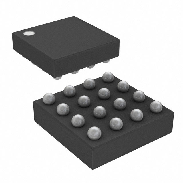


 工商网监
湘ICP备2023018690号
工商网监
湘ICP备2023018690号
