Product
Folder
Sample &
Buy
Support &
Community
Tools &
Software
Technical
Documents
LM3699
SNVS821A – JANUARY 2014 – REVISED MARCH 2014
LM3699 High-Efficiency White LED Driver
1 Features
3 Description
•
The LM3699 is a three-string, high-efficiency, PWMcontrolled power source for display backlight or
keypad LEDs in smartphone handsets. The highvoltage inductive boost converter with integrated 1-A,
40-V MOSFET provides the power for three series
LED strings. The boost output automatically adjusts
to LED forward voltage to minimize headroom voltage
and effectively improve LED efficiency.
1
•
•
•
•
•
•
•
•
•
•
•
Drives Parallel High-Voltage LED Strings for
Display or Keypad Lighting
Boost Converter up to 90% Efficiency
Four User-Selectable Full-Scale Current Settings
(20.2 mA, 18.6 mA, 17.0 mA, 15.4 mA)
Quick-Dimming Enable Terminal (ILOW)
Simple PWM Duty Cycle Control
24-V Overvoltage Protection Threshold
Fixed 1-MHz Switching Frequency
Integrated 1-A/40-V MOSFET
Three Current Sink Terminals
Adaptive Boost Output to LED Voltages
Thermal Shutdown Protection
29-mm2 Total Solution Size
The ILOW terminal provides a method to quickly
reduce LED brightness during camera flash
operation.
The LM3699 has integrated overvoltage, overcurrent,
and thermal protection.
The device operates over a 2.7-V to 5.5-V input
voltage range and a −40°C to 85°C temperature
range.
Device Information
2 Applications
•
•
Power Source for Smart Phone Illumination
Display or Keypad Illumination
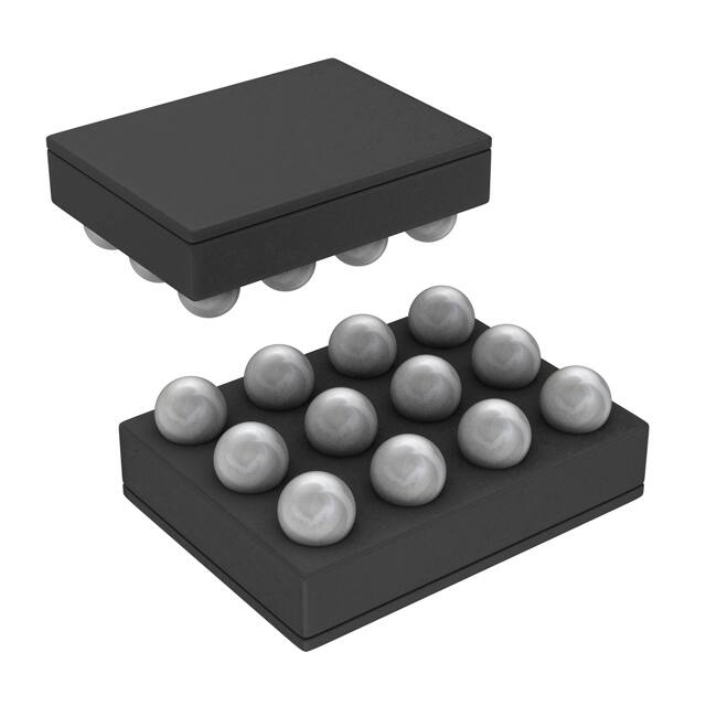
LM3699YFQ
PACKAGE
BODY SIZE
DSBGA (12)
1,64 mm x 1,29 mm
Boost Efficiency vs VIN with 10-µH Inductor
Simplified Schematic
L
ORDER NUMBER
D1
90%
VOUT up to 24V
VIN
CIN
88%
COUT
IN
SW
OVP
IS1
IS0
LM3699
HVLED1
ILOW
ILOW
HVLED2
RST
HWEN
HVLED3
PWM
EFFICIENCY (%)
86%
84%
82%
80%
78%
3s3p
76%
4s3p
74%
5s3p
72%
PWM
6s3p
GND
70%
2.5
3
3.5
4
4.5
5
5.5
VIN (V)
C012
1
An IMPORTANT NOTICE at the end of this data sheet addresses availability, warranty, changes, use in safety-critical applications,
intellectual property matters and other important disclaimers. PRODUCTION DATA.
�LM3699
SNVS821A – JANUARY 2014 – REVISED MARCH 2014
www.ti.com
Table of Contents
1
2
3
4
5
6
7
Features ..................................................................
Applications ...........................................................
Description .............................................................
Revision History.....................................................
Terminal Configuration and Functions................
Specifications.........................................................
1
1
1
2
3
4
6.1
6.2
6.3
6.4
6.5
6.6
4
4
4
4
5
7
Absolute Maximum Ratings ......................................
Handling Ratings.......................................................
Recommended Operating Conditions.......................
Thermal Information ..................................................
Electrical Characteristics ..........................................
Typical Characteristics ..............................................
Detailed Description .............................................. 8
7.1 Overview ................................................................... 8
7.2 Functional Block Diagram ......................................... 8
7.3 Feature Description................................................... 8
7.4 Device Functional Modes.......................................... 9
8
Application and Implementation ........................ 10
8.1 Application Information............................................ 10
8.2 Typical Application .................................................. 10
9 Power Supply Recommendations...................... 15
10 Layout................................................................... 16
10.1 Layout Guidelines ................................................ 16
10.2 Layout Example .................................................... 18
11 Device and Documentation Support ................. 19
11.1
11.2
11.3
11.4
Device Support......................................................
Trademarks ...........................................................
Electrostatic Discharge Caution ............................
Glossary ................................................................
19
19
19
19
12 Mechanical, Packaging, and Orderable
Information ........................................................... 19
4 Revision History
Changes from Original (January 2014) to Revision A
Page
•
Changed to new TI data sheet format: adding Handling Ratings table and Device and Documentation Support sections .. 1
•
Added new scope shot ........................................................................................................................................................ 14
2
Submit Documentation Feedback
Copyright © 2014, Texas Instruments Incorporated
Product Folder Links: LM3699
�LM3699
www.ti.com
SNVS821A – JANUARY 2014 – REVISED MARCH 2014
5 Terminal Configuration and Functions
DSBGA (YFQ)
12 Terminals
Bottom View
Top View
A
B
C
D
3
3
2
2
1
1
D
C
B
A
Terminal Functions
TERMINAL
DESCRIPTION
NUMBER
NAME
A1
PWM
A2
IS0
A3
HWEN
Hardware enable input. Drive this terminal high to enable the device. Drive this terminal low to force the
device into a low-power shutdown. HWEN is a high-impedance input and cannot be left floating.
B1
HVLED1
Input terminal to high-voltage current sink 1 (24 V max). The boost converter regulates the minimum of
HVLED1, HVLED2, and HVLED3 to VHR.
B2
IS1
Current select input 2. This is a high-impedance input and cannot be left floating. IS1 can be connected to
IN or GND.
B3
IN
Input voltage connection. Bypass IN to GND with a minimum 2.2-µF ceramic capacitor.
C1
HVLED2
C2
ILOW
Low level current enable. Drive this terminal high to reduce LED current by approximately 95%. ILOW is a
high-impedance input and cannot be left floating. If not used connect to GND.
C3
GND
Ground.
D1
HVLED3
Input terminal to high-voltage current sink 3 (24 V max). The boost converter regulates the minimum of
HVLED1, HVLED2, and HVLED3 to VHR.
D2
OVP
Overvoltage sense input. Connect OVP to the positive terminal of the inductive boost output capacitor
(COUT).
D3
SW
Drain connection for the internal NFET. Connect SW to the junction of the inductor and the Schottky diode
anode.
PWM brightness control input. PWM is a high-impedance input and cannot be left floating.
Current select input 1. This is a high-impedance input and cannot be left floating. IS0 can be connected to
IN or GND.
Input terminal to high-voltage current sink 2 (24 V max). The boost converter regulates the minimum of
HVLED1, HVLED2, and HVLED3 to VHR.
Submit Documentation Feedback
Copyright © 2014, Texas Instruments Incorporated
Product Folder Links: LM3699
3
�LM3699
SNVS821A – JANUARY 2014 – REVISED MARCH 2014
www.ti.com
6 Specifications
6.1 Absolute Maximum Ratings
over operating free-air temperature range (unless otherwise noted)
(1) (2)
MIN
MAX
VIN to GND
−0.3V
6
VSW, VOVP, VHVLED1, VHVLED2, VHVLED3 to GND
−0.3V
45
VIS1, VIS0, VILOW, VPWM to GND
−0.3V
6
VHWEN to GND
−0.3V
6
Continuous power dissipation
260 (peak)
Junction temperature (TJ-MAX)
(2)
V
Internally Limited
Maximum lead temperature (soldering)
(1)
UNIT
150
°C
Stresses beyond those listed under Absolute Maximum Ratings may cause permanent damage to the device. These are stress ratings
only, which do not imply functional operation of the device at these or any other conditions beyond those indicated under Recommended
Operating Conditions. Exposure to absolute-maximum-rated conditions for extended periods may affect device reliability.
All voltages are with respect to the potential at the GND terminal.
6.2 Handling Ratings
Storage temperature range
ESD Ratings (1)
(1)
(2)
(3)
MIN
MAX
−65
150
°C
2.0
kV
1500
V
Human body model (HBM) (2)
Charged device model (CDM) (3)
UNIT
Electrostatic discharge (ESD) to measure device sensitivity and immunity to damage caused by assembly line electrostatic discharges in
to the device.
Level listed above is the passing level per ANSI, ESDA, and JEDEC JS-001. JEDEC document JEP155 states that 500-V HBM allows
safe manufacturing with a standard ESD control process.
Level listed above is the passing level per EIA-JEDEC JESD22-C101. JEDEC document JEP157 states that 250-V CDM allows safe
manufacturing with a standard ESD control process.
6.3 Recommended Operating Conditions
over operating free-air temperature range (unless otherwise noted)
VIN to GND
VSW, VOVP, VHVLED1, VVHLED2, VVHLED3 to GND
Junction temperature (TJ)
(1)
(2)
(1) (2)
MIN
MAX
2.7
5.5
0
24
−40
125
UNIT
V
°C
Internal thermal shutdown circuitry protects the device from permanent damage. Thermal shutdown engages at TJ= 140°C (typ) and
disengages at TJ = 125°C (typ).
In applications where high power dissipation and/or poor package thermal resistance is present, the maximum ambient temperature may
have to be derated. Maximum ambient temperature (TA-MAX) is dependent on the maximum operating junction temperature (TJ-MAX-OP =
125°C), the maximum power dissipation of the device in the application (PD-MAX), and the junction-to ambient thermal resistance of the
part/package in the application (θJA), as given by the following equation: TA-MAX = TJ-MAX-OP – (θJA × PD-MAX).
6.4 Thermal Information
THERMAL METRIC (1)
RθJA
(1)
4
Junction-to-ambient thermal resistance
DSBGA
(12 TERMINALS)
55
UNIT
°C/W
For more information about traditional and new thermal metrics, see the IC Package Thermal Metrics application report, SPRA953.
Submit Documentation Feedback
Copyright © 2014, Texas Instruments Incorporated
Product Folder Links: LM3699
�LM3699
www.ti.com
SNVS821A – JANUARY 2014 – REVISED MARCH 2014
6.5 Electrical Characteristics
Limits apply over the full operating ambient temperature range (−40°C ≤ TA ≤ 85°C) and VIN = 3.6V, unless otherwise
specified. (1) (2)
SYMBOL
PARAMETER
TEST CONDITIONS
MIN
TYP
MAX
UNIT
General
2.7 V ≤ VIN ≤ 5.5 V, HWEN = GND
ISHDN
Shutdown current
3.0
2.7 V ≤ VIN ≤ 5.5 V, HWEN = GND,
TA = 25°C
Thermal shutdown
TSD
µA
1
140
Hysteresis
°C
15
Boost Converter
2.7 V ≤ VIN ≤ 5.5 V, ILOW = GND,
IS0 = IS1 = VIN,
PWM Duty Cycle = 100%
18.38
2.7 V ≤ VIN ≤ 5.5 V, ILOW = GND,
IS0 = IS1 = VIN,
PWM Duty Cycle = 100%
TA = 25°C
IHVLED(1/2/3)
Output current
regulation (HVLED1,
HVLED2, HVLED3)
ILOW = GND, IS0 = IS1 = VIN,
PWM Duty Cycle = 100%
TA = 25°C
20.2
18.7
20.2
18.63
3.0 V ≤ VIN ≤ 4.5 V, ILOW = GND,
IS0 = IS1 = VIN,
PWM Duty Cycle = 100%
TA = 25°C
2.7 V ≤ VIN ≤ 5.5 V, ILOW = GND,
IS0 = IS1 = VIN,
PWM Duty Cycle = 100%
IMATCH_HV
VREG_CS
VHR_MIN
HVLED matching
(HVLED1 to HVLED2
ILOW = GND, IS0 = IS1 = VIN,
or HVLED2 to HVLED3 PWM Duty Cycle = 100%, TA =
or HVLED1 to
25°C
HVLED3) (3)
3.0 V ≤ VIN ≤ 4.5 V, ILOW = GND,
IS0 = IS1 = VIN,
PWM Duty Cycle = 100%
Regulated current sink
headroom voltage
Minimum current sink
headroom voltage for
HVLED current sinks
RDSON
NMOS switch on
resistance
ICL_BOOST
NMOS Switch Current
Limit
(1)
(2)
(3)
21.58
mA
ILOW = GND, IS0 = IS1 = VIN,
PWM Duty Cycle = 100%,
TA = 25°C
3.0 V ≤ VIN ≤ 4.5 V, ILOW = GND,
IS0 = IS1 = VIN,
PWM Duty Cycle = 100%
TA = 25°C
22.02
21.58
20.2
–2.5%
2.5%
–2%
1.7%
–2.5%
2.5%
ILOW = GND, IS0 = IS1 = VIN,
PWM Duty Cycle = 100%,
TA = 25°C
400
ILED = 95% of nominal, ILOW =
GND, IS0 = IS1 = VIN, PWM Duty
Cycle = 100%
275
ILED = 95% of nominal, ILOW =
GND, IS0 = IS1 = VIN, PWM Duty
Cycle = 100%
TA = 25°C
190
ISW = 500 mA, TA = 25°C
0.3
880
TA = 25°C
Ω
1120
1000
mV
mA
All voltages are with respect to the potential at the GND terminal.
Minimum (Min) and Maximum (Max) limits are verified by design, test, or statistical analysis. Typical (Typ) numbers are not verified, but
do represent the most likely norm. Unless otherwise specified, conditions for typical specifications are: VIN = 3.6 V and TA = 25°C.
LED current sink matching in the high-voltage current sinks (HVLED1, HVLED2, and HVLED3) is given as the maximum matching value
between any two current sinks, where the matching between any two high-voltage current sinks (X and Y) is given as (IHVLEDX (or
IHVLEDY) - IAVE(X-Y))/(IAVE(X-Y)) x 100.
Submit Documentation Feedback
Copyright © 2014, Texas Instruments Incorporated
Product Folder Links: LM3699
5
�LM3699
SNVS821A – JANUARY 2014 – REVISED MARCH 2014
www.ti.com
Electrical Characteristics (continued)
Limits apply over the full operating ambient temperature range (−40°C ≤ TA ≤ 85°C) and VIN = 3.6V, unless otherwise
specified.(1)(2)
SYMBOL
PARAMETER
TEST CONDITIONS
ON threshold, 2.7 V ≤ VIN ≤ 5.5 V
Output overvoltage
protection
VOVP
fSW
Switching frequency
DMAX
MIN
TYP
23
UNIT
25
ON threshold, TA = 25°C
24
Hysteresis, TA = 25°C
0.7
2.7 V ≤ VIN ≤ 5.5 V
MAX
900
V
1100
TA = 25°C
1000
Maximum duty cycle
TA = 25°C
94%
Input logic low
2.7 V ≤ VIN ≤ 5.5 V
0
0.4
Input logic high
2.7 V ≤ VIN ≤ 5.5 V
1.2
VIN
VPWM_L
Input logic low
2.7 V ≤ VIN ≤ 5.5 V
0
0.4
VPWM_H
Input logic high
2.7 V ≤ VIN ≤ 5.5 V
1.31
VIN
tPWM
Minimum PWM input
pulse detected
2.7 V ≤ VIN ≤ 5.5 V
kHz
HWEN Input
VHWEN
V
PWM Input
0.75
V
µs
IS1, IS0, ILOW Inputs
VIL
Input logic low
2.7 V ≤ VIN ≤ 5.5 V
0
0.4
VIH
Input logic high
2.7 V ≤ VIN ≤ 5.5 V
1.29
VIN
1.7
2.1
V
Internal POR Threshold
VPOR
6
POR reset release
voltage threshold
VIN ramp time = 100 μs
VIN ramp time = 100 μs
TA = 25°C
Submit Documentation Feedback
1.9
V
Copyright © 2014, Texas Instruments Incorporated
Product Folder Links: LM3699
�LM3699
www.ti.com
SNVS821A – JANUARY 2014 – REVISED MARCH 2014
6.6 Typical Characteristics
2.5
0.5
2
IQ Shutdown (uA)
Rdson (Ohms)
0.45
0.4
0.35
0.3
0.2
-50
-25
0
25
50
75
100
1
0.5
VIN=2.7
VIN=3.6
VIN=5.5
0.25
1.5
VIN=5.5
VIN=3.6
VIN=2.7
0
-50
125
-25
0
Temperature (C)
25
50
75
100
125
Temperature (C)
C022
C024
Figure 1. Rdson vs Temperature
Figure 2. IQ Shutdown vs Temperature
300
2
POR Threshold (V)
VHEADROOM (mV)
250
200
150
100
1.5
1
0.5
VIN=2.7
VIN=3.6
VIN=5.5
50
0
-50
-25
0
25
50
75
100
VIN=3.6
0
-50
125
-25
0
Temperature (C)
25
50
75
100
125
Temperature (C)
C027
C023
Figure 4. POR Threshold vs Temperature
1.4
1.2
1.2
1
1
PWM VIL (V)
PWM VIH (V)
Figure 3. VHR_MIN vs Temperature
1.4
0.8
0.6
0.4
0.8
0.6
0.4
VIN=5.5
VIN=3.6
VIN=2.7
0.2
0
-50
-25
0
25
50
75
100
VIN=5.5
VIN=3.6
VIN=2.7
0.2
0
125
Temperature (C)
-50
-25
0
25
50
75
100
125
Temperature (C)
C026
C025
Figure 5. PWM VIH vs Temperature
Figure 6. PWM VIL vs Temperature
Submit Documentation Feedback
Copyright © 2014, Texas Instruments Incorporated
Product Folder Links: LM3699
7
�LM3699
SNVS821A – JANUARY 2014 – REVISED MARCH 2014
www.ti.com
7 Detailed Description
7.1 Overview
The LM3699 provides power for three high-voltage LED strings. The high-voltage LED strings are powered from
an integrated boost converter. The LED current is directly controlled by a Pulse Width Modulation (PWM) input.
7.2 Functional Block Diagram
IN
SW
Overvoltage
Protection
HWEN
Hardware Enable,
Reference, and
Thermal Shutdown
Boost Converter
OVP
Current Limit
Switch Frequency
High Voltage
Current Sinks
LPF
PWM
HVLED1
IS1
HVLED2
Full-Scale
Current
Control
IS0
HVLED3
GND
Quick
Dimming
Control
ILOW
7.3 Feature Description
7.3.1 PWM Input
The active high PWM input is filtered by an internal low-pass filter, then converted to an analog control voltage to
set the current level on the current sink outputs. The PWM input is high-impedance and cannot be left floating.
7.3.1.1 PWM Input Frequency Range
The usable input frequency range for the PWM input is governed on the low end by the cutoff frequency of the
internal low-pass filter (540 Hz, Q = 0.33) and on the high end by the propagation delays through the internal
logic. For frequencies below 2 kHz the current ripple begins to become a larger portion of the DC LED current.
Additionally, at lower PWM frequencies the boost output voltage ripple increases, causing a non-linear response
from the PWM duty cycle to the average LED current due to the response time of the boost. For the best
response of current vs. duty cycle, the PWM input frequency should be kept between 2 kHz and 100 kHz.
7.3.1.2 PWM Low Detect
The LM3699 incorporates a feature to detect when the PWM input duty cycle is near zero. This feature requires
that the minimum PWM input pulse width be greater than tPWM (see Electrical Characteristics ). A PWM input
pulse width less than tPWM can result in the current sink outputs turning on and off resulting in flicker on the
LEDs.
8
Submit Documentation Feedback
Copyright © 2014, Texas Instruments Incorporated
Product Folder Links: LM3699
�LM3699
www.ti.com
SNVS821A – JANUARY 2014 – REVISED MARCH 2014
Feature Description (continued)
7.3.2 HWEN Input
HWEN is the global hardware enable to the LM3699 and must be driven high to enable the device. HWEN is a
high-impedance input, so it cannot be left floating. When HWEN is driven low the LM3699 is placed in shutdown,
and the boost converter and all the HVLED current sinks are turned off.
7.3.3 Current Select Inputs (IS1 And IS0)
The current select inputs IS1 and IS0 select the maximum full-scale current (ifs). These digital inputs are static
and must not change state when HWEN > VIL. IS1 and IS0 are high-impedance inputs so they cannot be left
floating. The terminals IS1 and IS0 can be connected directly to IN or GND and do not require an external
pullup/pulldown resistor. The full-scale current is set according to Table 1:
Table 1. Full-Scale Current vs Current Select Inputs IS1 and IS0
IS1
IS0
FULL-SCALE CURRENT (ifs) (mA)
0
0
15.4
0
1
17.0
1
0
18.6
1
1
20.2
7.3.4 ILOW Input
The ILOW feature provides a way to quickly reduce the LED current. This feature can be used to dim the LCD
backlight during camera flash operation without changing the PWM duty cycle. ILOW is a high-impedance input
so it cannot be left floating. When ILOW is driven high, the high-voltage current sink outputs are approximately
equal to (ifs x DPWM x 5%). When ILOW is driven low, the high-voltage current sinks are a function of the fullscale current setting and the PWM input duty cycle. If ILOW is not required the input should be connected to
GND.
7.3.5 Thermal Shutdown
The LM3699 contains a thermal shutdown protection. In the event the die temperature reaches 140°C (typ), the
boost converter and current sink outputs shut down until the die temperature drops to typically 125°C.
7.4 Device Functional Modes
7.4.1 Operation with an Unused Current Sink
If one of the current sink outputs is not connected to a LED string the terminal must be connected to VIN. This
ensures that the boost converter regulates the headroom voltage on the highest voltage LED string.
Submit Documentation Feedback
Copyright © 2014, Texas Instruments Incorporated
Product Folder Links: LM3699
9
�LM3699
SNVS821A – JANUARY 2014 – REVISED MARCH 2014
www.ti.com
8 Application and Implementation
8.1 Application Information
Table 2. Recommended Components
VALUE
PART NUMBER
SIZE (mm)
CURRENT/VOLTAGE
RATING (RESISTANCE)
TDK
10 µH
VLF302512MT-100M
2.5 x 3.0 x 1.2
620 mA/0.25 Ω
TDK
1.0 µF
C2012X5R1E105
0805
25V
COMPONENT
MANUFACTURER
L
COUT
CIN
TDK
2.2 µF
C1005X5R1A225
0402
10V
Diode
On-Semi
Schottky
NSR0240V2T1G
SOD-523
40V, 250 mA
8.2 Typical Application
VIN = 2.7 - 5.5 V
VIN
L1
VLF302512MT-100M
10µH
D1
NSR0240V2T1G
SW
40V
CIN
2.2µF
U2
LM3699YFQ
B2
A2
A3
HWEN
A1
PWM
C2
ILOW
IN
SW
OVP
IS1
IS0
HWEN
D3
VOUT
D2
1
B3
GND
COUT
1µF
PWM
HVLED1
HVLED2
HVLED3
ILOW
GND
B1
C1
D1
LED1
LED2
LED3
GND
C3
GND
Figure 7. LM3699 Simplified Schematic
8.2.1 Design Requirements
Table 3. Design Parameters
DESIGN PARAMETER
EXAMPLE VALUE
Full-scale current setting
20.2 mA
Minimum input voltage
2.7 V
LED series/parallel configuration
6s3p
LED maximum forward voltage (Vf)
3.5 V
Efficiency
75%
8.2.2 Detailed Design Procedure
8.2.2.1 Step-by-Step Design Procedure
The designer needs to know the following:
• Full-scale current setting
• Minimum input voltage
• LED series/parallel configuration
• LED maximum forward voltage (Vf)
• LM3699 efficiency for LED configuration
10
Submit Documentation Feedback
Copyright © 2014, Texas Instruments Incorporated
Product Folder Links: LM3699
�LM3699
www.ti.com
SNVS821A – JANUARY 2014 – REVISED MARCH 2014
The full-scale current setting, number of series LEDs, and minimum input voltage are needed in order to
calculate the peak input current, maximum output voltage, and maximum required output power. This information
guides the designer to determine if the LM3699 can support the required output power and make the appropriate
inductor selection for the application.
The LM3699 Boost converter output voltage (VOUT) is calculated as follows:
number of series LEDs x Vf + 0.4V
The LM3699 Boost converter output current (IOUT) is calculated as follows:
number of parallel LED strings x full-scale current
The LM3699 peak input current (IIN_PK) is calculated as follows:
VOUT u IOUT / Minimum VIN / Efficiency
VOUT
21.4 V
6 u 3.5 V � 0.4 V
IOUT
0.0606 A
0.0202 A u 3
IIN _PK ! 0.640 A
21.4 V u 0.0606 A / 2.7 V / 0.75
(1)
8.2.2.2 Maximum Output Power
The maximum output power of the device is governed by two factors: the peak current limit (ICL = 880 mA min)
and the maximum output voltage (VOUT). When the application causes either of these limits to be reached, it is
possible that the proper current regulation and matching between LED current strings will not be met.
8.2.2.2.1 Peak Current Limited
In the case of a peak current limited situation, when the peak of the inductor current hits the LM3699 current
limit, the NFET switch turns off for the remainder of the switching period. If this happens each switching cycle the
LM3699 regulates the peak of the inductor current instead of the headroom across the current sinks. This can
result in the dropout of the current sinks, and the LED current dropping below its programmed level.
The peak current (IPEAK) in a boost converter is dependent on the value of the inductor, total LED current in the
boost (IOUT), the boost output voltage (VOUT) (which is the highest voltage LED string + VHR ), the input voltage
(VIN), the switching frequency (ƒSW), and the efficiency (Output Power/Input Power). Additionally, the peak
current is different depending on whether the inductor current is continuous during the entire switching period
(CCM), or discontinuous (DCM) where it goes to 0 before the switching period ends. For CCM, the peak inductor
current is given by:
IPEAK =
IOUT x VOUT
+
VIN x efficiency
VIN
2 x ¦SW x L
x 1-
VIN x efficiency
VOUT
(2)
For DCM the peak inductor current is given by:
2 u IOUT
IPEAK =
´
¶ SW
u L u efficiency
u §VOUT - VIN u efficiency·
©
¹
(3)
To determine which mode the circuit is operating in (CCM or DCM) a calculation must be done to test whether
the inductor current ripple is less than the anticipated input current (IIN). If ΔIL is less than IIN, then the device is
operating in CCM. If ΔIL is greater than IIN then the device is operating in DCM.
IOUT u VOUT
VIN u efficiency
>
VIN
´
¶SW
uL
u §1 �
©
VIN u efficiency ·
VOUT
¹
(4)
Typically at currents high enough to reach the LM3699 peak current limit, the device operates in CCM.
Figure 8 shows the output current derating for a 10-µH and a 22-µH inductor using 75% and 80% efficiency
estimates. These plots take equations (2) and (3) from above and plot IOUT with varying VIN using a constant
peak current of 880 mA (ICL_MIN) and 1-MHz switching frequency. Using these curves can help the user
understand the impact of VIN, inductance, and efficiency on the maximum output current. A 10-µH inductor can
typically be a smaller device with lower on resistance, but the peak currents will be higher. A 22-µH inductor
provides for lower peak currents, but to match the DC resistance of a 10-µH inductor requires a larger sized
device.
Submit Documentation Feedback
Copyright © 2014, Texas Instruments Incorporated
Product Folder Links: LM3699
11
�LM3699
SNVS821A – JANUARY 2014 – REVISED MARCH 2014
www.ti.com
0.062
0.061
0.06
IOUT (A)
0.059
0.058
0.057
0.056
10uH 75% Eff
0.055
10uH 80% Eff
0.054
22uH 75% Eff
0.053
5.5
5.3
5.1
4.9
4.7
4.5
4.3
4.1
3.9
3.7
3.5
3.3
3.1
2.9
2.7
VIN (V)
C021
Figure 8. Maximum Output Power Vs Inductance And Efficiency
8.2.2.2.2 Output Voltage Limited
If a output voltage limited situation occurs, when the boost output voltage hits the LM3699 OVP threshold, the
NFET turns off and stays off until the output voltage falls below the hysteresis level (typically 1 V below the OVP
threshold). This results in the boost converter regulating the output voltage to the OVP threshold, causing the
current sinks to go into dropout. The LM3699 OVP setting supports LED strings up to 6 series LEDs (Vƒmax = 3.5
V).
8.2.2.3 Boost Inductor Selection
The boost converter operates using either a 10-µH or 22-µH inductor. The inductor selected must have a
saturation current greater than the peak operating current.
8.2.2.4 Output Capacitor Selection
The LM3699 inductive boost converter requires a 1.0-µF X5R or X7R 50V (0805 size) ceramic capacitor to filter
the output voltage. Pay careful attention to the capacitor tolerance and DC bias response. Smaller body-size 1.0µF ceramic capacitors or 25-V, 1.0-µF ceramic capacitors can be used, but for proper operation the degradation
in capacitance due to tolerance, DC bias, and temperature should stay above 0.4 µF. This might require placing
two devices in parallel in order to maintain the required output capacitance over the device operating range and
series LED configuration.
8.2.2.5 Schottky Diode Selection
The Schottky diode must have a reverse breakdown voltage greater than the LM3699’s maximum output voltage.
Additionally, the diode must have an average current rating high enough to handle the LM3699’s maximum
output current, and at the same time the diode peak current rating must be high enough to handle the peak
inductor current. Schottky diodes are required due to their lower forward voltage drop (0.3 V to 0.5 V) and their
fast recovery time.
8.2.2.6 Input Capacitor Selection
The LM3699 inductive boost converter requires a 2.2-µF X5R or X7R ceramic capacitor to filter the input voltage.
The input capacitor filters the inductor current ripple and the internal MOSFET driver currents during turnon of the
internal power switch.
12
Submit Documentation Feedback
Copyright © 2014, Texas Instruments Incorporated
Product Folder Links: LM3699
�LM3699
www.ti.com
SNVS821A – JANUARY 2014 – REVISED MARCH 2014
8.2.3 Application Performance Plots
92%
90%
90%
88%
88%
86%
86%
EFFICIENCY (%)
EFFICIENCY (%)
VIN = 3.6 V, LEDs are WLEDs part # SML-312WBCW(A), Typical Application Circuit with L = TDK (VLF302512, 10 µH, 22 µH
where specified), Schottky = On-Semi (NSR0240V2T1G), TA = 25°C unless otherwise specified. Efficiency is given as (VOUT ×
(IHVLED1 + IHVLED2+ IHVLED3))/(VIN × IIN), matching curves are given as (ΔILED_MAX/ILED_AVE).
84%
82%
80%
78%
3s3p
76%
4s3p
74%
2.5
3
3.5
4
4.5
5
80%
78%
3s3p
76%
4s3p
5s3p
72%
6s3p
70%
82%
74%
5s3p
72%
84%
6s3p
70%
5.5
2.5
3
3.5
VIN (V)
4
4.5
5
5.5
VIN (V)
C013
L = 22 µH
C012
20 mA/String
L = 10 µH
Figure 10. Boost Efficiency vs VIN
92.0%
90.0%
90.0%
88.0%
88.0%
86.0%
86.0%
EFFICIENCY (%)
EFFICIENCY (%)
Figure 9. Boost Efficiency vs VIN
84.0%
82.0%
80.0%
78.0%
76.0%
3s3p
4s3p
5s3p
6s3p
74.0%
72.0%
70.0%
0
12
24
36
48
20 mA/String
84.0%
82.0%
80.0%
78.0%
76.0%
3s3p
4s3p
5s3p
6s3p
74.0%
72.0%
70.0%
0
60
12
24
ILED (mA)
36
48
60
ILED (mA)
C004
C003
Figure 11. LED Efficiency vs ILED
Figure 12. LED Efficiency vs ILED
1.70
1.01
1.00
1.50
-40°C
0.99
85°C
PEAK CURRENT (A)
1.10
-40°C
0.90
25°C
0.70
25°C
0.97
0.96
85°C
0.95
0.94
0.93
0.92
0.91
0.90
5.50
5.25
5.00
4.75
4.50
4.25
VIN (V)
4.00
3.75
Figure 13. Shutdown Current vs VIN
3.50
C001
3.25
5.50
5.25
5.00
4.75
4.50
4.25
4.00
3.75
3.50
3.25
3.00
2.75
2.50
VIN (V)
3.00
0.50
2.75
2.50
SHUTDOWN CURRENT (uA)
0.98
1.30
C001
Figure 14. Open Loop Current Limit vs VIN
Submit Documentation Feedback
Copyright © 2014, Texas Instruments Incorporated
Product Folder Links: LM3699
13
�LM3699
SNVS821A – JANUARY 2014 – REVISED MARCH 2014
www.ti.com
VIN = 3.6 V, LEDs are WLEDs part # SML-312WBCW(A), Typical Application Circuit with L = TDK (VLF302512, 10 µH, 22 µH
where specified), Schottky = On-Semi (NSR0240V2T1G), TA = 25°C unless otherwise specified. Efficiency is given as (VOUT ×
(IHVLED1 + IHVLED2+ IHVLED3))/(VIN × IIN), matching curves are given as (ΔILED_MAX/ILED_AVE).
100.00%
RIPPLE CURRENT (%)
10.00%
1.00%
0.10%
0.01%
DPWM = 50%
3 x 6 LEDs
10000
8000
6000
4000
2000
0
PWM FREQUENCY (Hz)
DPWM = 100%
3 x 6 LEDs
Figure 16. Start-Up Response
20 mA/String
3p6s
20.2 mA/String
Figure 17. Start-Up Response
3p6s
20.2 mA/String
DPWM = 30% to 90%
ƒ = 10 kHz
Figure 18. DPWM Step Change Response
DPWM = 100%
3p6s
4.2 V to 3.6 V
20.2 mA/String
DPWM = 100%
Figure 20. VIN Step Response
Figure 19. VIN Step Response
14
20 mA/String
20 mA/String
Figure 15. LED Current Ripple vs FPWM
DPWM = 0%
3 x 6 LEDs
C001
Submit Documentation Feedback
Copyright © 2014, Texas Instruments Incorporated
Product Folder Links: LM3699
�LM3699
www.ti.com
SNVS821A – JANUARY 2014 – REVISED MARCH 2014
VIN = 3.6 V, LEDs are WLEDs part # SML-312WBCW(A), Typical Application Circuit with L = TDK (VLF302512, 10 µH, 22 µH
where specified), Schottky = On-Semi (NSR0240V2T1G), TA = 25°C unless otherwise specified. Efficiency is given as (VOUT ×
(IHVLED1 + IHVLED2+ IHVLED3))/(VIN × IIN), matching curves are given as (ΔILED_MAX/ILED_AVE).
3p6s
3.6 V to 4.2 V
20.2 mA/String
3p6s
DPWM = 100%
20.2 mA/String
DPWM = 50%
Figure 22. ILOW Disabled
Figure 21. VIN Step Response
3p6s
20.2 mA/String
DPWM = 50%
Figure 23. ILOW Enabled
9 Power Supply Recommendations
The LM3699 is designed to operate from an input voltage supply range of 2.7 V to 5.5 V. The input supply
connection must be properly designed to support the LM3699 maximum peak current limit.
Submit Documentation Feedback
Copyright © 2014, Texas Instruments Incorporated
Product Folder Links: LM3699
15
�LM3699
SNVS821A – JANUARY 2014 – REVISED MARCH 2014
www.ti.com
10 Layout
10.1 Layout Guidelines
The LM3699 inductive boost converter sees a high switched voltage (up to 24 V) at the SW terminal, as well as a
step current (up to 1 A) through the Schottky diode and output capacitor each switching cycle. The high switching
voltage can create interference into nearby nodes due to electric field coupling (I = CdV/dt). The large step
current through the diode and the output capacitor can cause a large voltage spike at the SW and OVP terminals
due to parasitic inductance in the step current conducting path (V = Ldi/dt). Board layout guidelines are geared
towards minimizing this electric field coupling and conducted noise. Figure 24 highlights these two noisegenerating components.
Voltage Spike
VOUT + VF Schottky
Pulsed voltage at SW
IPEAK
Current through
Schottky and
COUT
IAVE = IIN
Current through
Inductor
Parasitic
Circuit Board
Inductances
Affected Node
due to Capacitive Coupling
LCD Display
Cp1
L
Lp1
D1
Lp2
Up to 24V
2.7 V to 5.5 V
COUT
IN
SW
Lp3
CIN
LM3699
PWM
OVP
HWEN
ILOW
IS1
IS0
HVLED1
HVLED2
HVLED3
GND
Figure 24. LM3699 Inductive Boost Converter Showing Pulsed Voltage At SW (High dv/dt) And Current
Through Schottky And COUT (High di/dt)
The following list details the main (layout sensitive) areas of the LM3699 inductive boost converter in order of
decreasing importance:
1. Output Capacitor
– Schottky Cathode to COUT+
– COUT− to GND
2. Schottky Diode
– SW Terminal to Schottky Anode
– Schottky Cathode to COUT+
16
Submit Documentation Feedback
Copyright © 2014, Texas Instruments Incorporated
Product Folder Links: LM3699
�LM3699
www.ti.com
SNVS821A – JANUARY 2014 – REVISED MARCH 2014
Layout Guidelines (continued)
3. Inductor
– SW Node PCB capacitance to other traces
4. Input Capacitor
– CIN+ to IN terminal
10.1.1 Boost Output Capacitor Placement
Because the output capacitor is in the path of the inductor current discharge path, a high-current step from 0 to
IPEAK occurs each time the switch turns off and the Schottky diode turns on. Any inductance along this series
path from the cathode of the diode through COUT and back into the LM3699 GND terminal contributes to voltage
spikes (VSPIKE = LP_ × di/dt) at SW and OUT. These spikes can potentially over-voltage the SW terminal, or feed
through to GND. To avoid this, COUT+ must be connected as close as possible to the Cathode of the Schottky
diode, and COUT− must be connected as close as possible to the LM3699 GND terminal. The best placement for
COUT is on the same layer as the LM3699 so as to avoid any vias that can add excessive series inductance.
10.1.2 Schottky Diode Placement
In the boost circuit of the device the Schottky diode is in the path of the inductor current discharge. As a result
the Schottky diode sees a high-current step from 0 to IPEAK each time the switch turns off and the diode turns on.
Any inductance in series with the diode may cause a voltage spike (VSPIKE = LP_ × di/dt) at SW and OUT. This
can potentially over-voltage the SW terminal, or feed through to VOUT and through the output capacitor and into
GND. Connecting the anode of the diode as close as possible to the SW terminal and the cathode of the diode
as close as possible to COUT+ reduces the inductance (LP_) and minimize these voltage spikes.
10.1.3 Inductor Placement
The node where the inductor connects to the LM3699 SW terminal has 2 issues. First, a large switched voltage
(0 to VOUT + VF_SCHOTTKY) appears on this node every switching cycle. This switched voltage can be
capacitively coupled into nearby nodes. Second, there is a relatively large current (input current) on the traces
connecting the input supply to the inductor and connecting the inductor to the SW terminal. Any resistance in this
path can cause voltage drops that can negatively affect efficiency and reduce the input operating voltage range.
To reduce the capacitive coupling of the signal on SW into nearby traces, the SW terminal-to-inductor connection
must be minimized in area. This limits the PCB capacitance from SW to other traces. Additionally, highimpedance nodes that are more susceptible to electric field coupling need to be routed away from SW and not
directly adjacent or beneath. This is especially true for traces such as IS1, IS0, ILOW, HWEN, and PWM. A GND
plane placed directly below SW greatly reduce the capacitance from SW into nearby traces.
Lastly, limit the trace resistance of the VBATT-to-inductor connection and from the inductor-to-SW connection, by
use of short, wide traces.
10.1.4 Boost Input Capacitor Placement
For the LM3699 boost converter, the input capacitor filters the inductor current ripple and the internal MOSFET
driver currents during turnon of the internal power switch. The driver current requirement can range from 50 mA
at 2.7 V to over 200 mA at 5.5 V with fast durations of approximately 10 ns to 20 ns. This appears as high di/dt
current pulses coming from the input capacitor each time the switch turns on. Close placement of the input
capacitor to the IN terminal and to the GND terminal is critical since any series inductance between IN and CIN+
or CIN− and GND can create voltage spikes that could appear on the VIN supply line and in the GND plane.
Submit Documentation Feedback
Copyright © 2014, Texas Instruments Incorporated
Product Folder Links: LM3699
17
�LM3699
SNVS821A – JANUARY 2014 – REVISED MARCH 2014
www.ti.com
10.2 Layout Example
Figure 25 requires two PCB layers and is optimized for the GND connection.
Figure 25. LM3699 GND Optimized Layout Example
18
Submit Documentation Feedback
Copyright © 2014, Texas Instruments Incorporated
Product Folder Links: LM3699
�LM3699
www.ti.com
SNVS821A – JANUARY 2014 – REVISED MARCH 2014
11 Device and Documentation Support
11.1 Device Support
11.1.1 Third-Party Products Disclaimer
TI'S PUBLICATION OF INFORMATION REGARDING THIRD-PARTY PRODUCTS OR SERVICES DOES NOT
CONSTITUTE AN ENDORSEMENT REGARDING THE SUITABILITY OF SUCH PRODUCTS OR SERVICES
OR A WARRANTY, REPRESENTATION OR ENDORSEMENT OF SUCH PRODUCTS OR SERVICES, EITHER
ALONE OR IN COMBINATION WITH ANY TI PRODUCT OR SERVICE.
11.2 Trademarks
All trademarks are the property of their respective owners.
11.3 Electrostatic Discharge Caution
This integrated circuit can be damaged by ESD. Texas Instruments recommends that all integrated circuits be handled with
appropriate precautions. Failure to observe proper handling and installation procedures can cause damage.
ESD damage can range from subtle performance degradation to complete device failure. Precision integrated circuits may be more
susceptible to damage because very small parametric changes could cause the device not to meet its published specifications.
11.4 Glossary
SLYZ022 — TI Glossary.
This glossary lists and explains terms, acronyms and definitions.
12 Mechanical, Packaging, and Orderable Information
The following pages include mechanical, packaging, and orderable information. This information is the most
current data available for the designated devices. This data is subject to change without notice and revision of
this document. For browser-based versions of this data sheet, refer to the left-hand navigation.
Submit Documentation Feedback
Copyright © 2014, Texas Instruments Incorporated
Product Folder Links: LM3699
19
�PACKAGE OPTION ADDENDUM
www.ti.com
10-Dec-2020
PACKAGING INFORMATION
Orderable Device
Status
(1)
Package Type Package Pins Package
Drawing
Qty
Eco Plan
(2)
Lead finish/
Ball material
MSL Peak Temp
Op Temp (°C)
Device Marking
(3)
(4/5)
(6)
LM3699YFQR
ACTIVE
DSBGA
YFQ
12
3000
RoHS & Green
SNAGCU
Level-1-260C-UNLIM
-40 to 125
D9
(1)
The marketing status values are defined as follows:
ACTIVE: Product device recommended for new designs.
LIFEBUY: TI has announced that the device will be discontinued, and a lifetime-buy period is in effect.
NRND: Not recommended for new designs. Device is in production to support existing customers, but TI does not recommend using this part in a new design.
PREVIEW: Device has been announced but is not in production. Samples may or may not be available.
OBSOLETE: TI has discontinued the production of the device.
(2)
RoHS: TI defines "RoHS" to mean semiconductor products that are compliant with the current EU RoHS requirements for all 10 RoHS substances, including the requirement that RoHS substance
do not exceed 0.1% by weight in homogeneous materials. Where designed to be soldered at high temperatures, "RoHS" products are suitable for use in specified lead-free processes. TI may
reference these types of products as "Pb-Free".
RoHS Exempt: TI defines "RoHS Exempt" to mean products that contain lead but are compliant with EU RoHS pursuant to a specific EU RoHS exemption.
Green: TI defines "Green" to mean the content of Chlorine (Cl) and Bromine (Br) based flame retardants meet JS709B low halogen requirements of


 工商网监
湘ICP备2023018690号
工商网监
湘ICP备2023018690号

