Product
Folder
Sample &
Buy
Support &
Community
Tools &
Software
Technical
Documents
LM4041-N, LM4041-N-Q1
SNOS641G – OCTOBER 1999 – REVISED JANUARY 2016
LM4041-N-xx Precision Micropower Shunt Voltage Reference
1 Features
3 Description
•
•
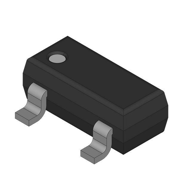
Ideal for space-critical applications, the LM4041-N
precision voltage reference is available in the subminiature SC70 and SOT-23 surface-mount
packages. The advanced design of the LM4041-N
eliminates the need for an external stabilizing
capacitor while ensuring stability with any capacitive
load, thus making the LM4041-N easy to use. Further
reducing design effort is the availability of a fixed
(1.225 V) and adjustable reverse breakdown voltage.
The minimum operating current is 60 μA for the
LM4041-N 1.2 and the LM4041-N ADJ. Both versions
have a maximum operating current of 12 mA.
1
•
•
•
•
•
•
•
•
•
•
•
Qualified for Automotive Applications
SEC-Q100 Qualified With the Following Results:
– Device Temperature Grade 1: –40°C to
+125°C Ambient Temperature Range
– Device Temperature Grade 3: –40°C to +85°C
Ambient Temperature Range (For SOT-23
Only)
Available in Standard, AEC Q-100 Grade 1
(Extended Temperature Range), and Grade 3
(Industrial Temperature Range) Qualified Versions
(SOT-23 Only)
Small Packages: SOT-23, TO-92, and SC70
No Output Capacitor Required
Tolerates Capacitive Loads
Reverse Breakdown Voltage Options of 1.225 V
and Adjustable
Output Voltage Tolerance (A grade, 25°C) =
±0.1%(Maximum)
Low Output Noise (10 Hz to 10kHz) = 20 μVrms
Wide Operating Current Range of 60 μA to 12 mA
Industrial Temperature Range (LM4041A/B-N,
LM4041-N-Q1A/Q1B) of −40°C to +85°C
Extended Temperature Range (LM4041C/D/E-N,
LM4041-N-Q1C/Q1D/Q1E) of −40°C to +125°C
Low Temperature Coefficient of 100 ppm/°C
(Maximum)
2 Applications
•
•
•
•
•
•
•
The LM4041-N uses fuse and Zener-zap reverse
breakdown or reference voltage trim during wafer sort
to ensure that the prime parts have an accuracy of
better than ±0.1% (A grade) at 25°C. Bandgap
reference temperature drift curvature correction and
low dynamic impedance ensure stable reverse
breakdown voltage accuracy over a wide range of
operating temperatures and currents.
Device Information(1)
PART NUMBER
LM4041-N
LM4041-N-Q1
PACKAGE
BODY SIZE (NOM)
SC70 (5)
1.25 mm × 2.00 mm
SOT-23 (3)
1.30 mm × 2.92 mm
TO-92 (3)
4.30 mm × 4.30 mm
SOT-23 (3)
1.30 mm × 2.92 mm
(1) For all available packages, see the orderable addendum at
the end of the data sheet.
Block Diagram
Portable, Battery-Powered Equipment
Data Acquisition Systems
Instrumentation
Process Control
Energy Management
Automotive
Precision Audio Components
1
An IMPORTANT NOTICE at the end of this data sheet addresses availability, warranty, changes, use in safety-critical applications,
intellectual property matters and other important disclaimers. PRODUCTION DATA.
�LM4041-N, LM4041-N-Q1
SNOS641G – OCTOBER 1999 – REVISED JANUARY 2016
www.ti.com
Table of Contents
1
2
3
4
5
6
Features ..................................................................
Applications ...........................................................
Description .............................................................
Revision History.....................................................
Pin Configuration and Functions .........................
Specifications.........................................................
6.1
6.2
6.3
6.4
6.5
1
1
1
2
3
4
Absolute Maximum Ratings ...................................... 4
ESD Ratings.............................................................. 5
Recommended Operating Conditions....................... 5
Thermal Information .................................................. 5
LM4041-N-xx 1.2 Electrical Characteristics (Industrial
Temperature Range).................................................. 6
6.6 LM4041-N-xx 1.2 Electrical Characteristics (Industrial
Temperature Range).................................................. 7
6.7 LM4041-N-xx 1.2 Electrical Characteristics (Extended
Temperature Range).................................................. 9
6.8 LM4041-N-xx ADJ (Adjustable) Electrical
Characteristics (Industrial Temperature Range) ...... 11
6.9 LM4041-N-xx ADJ (Adjustable) Electrical
Characteristics (Extended Temperature Range) ..... 13
6.10 Typical Characteristics .......................................... 14
7
8
Parameter Measurement Information ................ 17
Detailed Description ............................................ 17
8.1
8.2
8.3
8.4
9
Overview .................................................................
Functional Block Diagram .......................................
Feature Description.................................................
Device Functional Modes........................................
17
17
17
18
Application and Implementation ........................ 19
9.1 Application Information............................................ 19
9.2 Typical Applications ................................................ 20
10 Power Supply Recommendations ..................... 27
11 Layout................................................................... 27
11.1 Layout Guidelines ................................................. 27
11.2 Layout Example .................................................... 27
12 Device and Documentation Support ................. 28
12.1
12.2
12.3
12.4
12.5
Related Links ........................................................
Community Resources..........................................
Trademarks ...........................................................
Electrostatic Discharge Caution ............................
Glossary ................................................................
28
28
28
28
28
13 Mechanical, Packaging, and Orderable
Information ........................................................... 28
4 Revision History
NOTE: Page numbers for previous revisions may differ from page numbers in the current version.
Changes from Revision F (July 2013) to Revision G
•
Page
Added ESD Ratings table, Feature Description section, Device Functional Modes, Application and Implementation
section, Power Supply Recommendations section, Layout section, Device and Documentation Support section, and
Mechanical, Packaging, and Orderable Information section ................................................................................................. 1
Changes from Revision D (April 2013) to Revision E
•
2
Page
Changed layout of National Data Sheet to TI format ........................................................................................................... 24
Submit Documentation Feedback
Copyright © 1999–2016, Texas Instruments Incorporated
Product Folder Links: LM4041-N LM4041-N-Q1
�LM4041-N, LM4041-N-Q1
www.ti.com
SNOS641G – OCTOBER 1999 – REVISED JANUARY 2016
5 Pin Configuration and Functions
DBZ Package
3-Pin SOT-23
Top View
DCK Package
5-Pin SC70
Top View
1
1
+
3*
5
t
N/C
2
2
N/C*
–
3
+
4
N/C
1.2 V
LP Package
3-Pin TO-92
Top View
Pin Functions
PIN
I/O
DESCRIPTION
NAME
SOT-23
SC70
TO-92
Anode
2
1
1
O
Anode pin, normally grounded
Cathode
1
3
2
I/O
Shunt current and output voltage
FB
—
—
—
I
NC**
3
2
—
—
**Must float or connect to anode
NC
—
4, 5
3
—
No connect
Feedback pin for adjustable output voltage
Copyright © 1999–2016, Texas Instruments Incorporated
Product Folder Links: LM4041-N LM4041-N-Q1
Submit Documentation Feedback
3
�LM4041-N, LM4041-N-Q1
SNOS641G – OCTOBER 1999 – REVISED JANUARY 2016
www.ti.com
DBZ Package
3-Pin SOT-23
Top View
DCK Package
5-Pin SC70
Top View
1
5
1
FB
3
FB
N/C
–
2
2
+
t
ADJ
4
3
N/C
+
ADJ
LP Pakage
3-Pin TO-92
Bottom View
Pin Functions: ADJ Pinouts
PIN
I/O
DESCRIPTION
NAME
SOT-23
SC70
TO-92
Anode
3
2
1
O
Anode pin, normally grounded
Cathode
2
3
2
I/O
Shunt current and output voltage
FB
1
5
3
I
NC**
—
—
—
—
Feedback pin for adjustable output voltage
**Must float or connect to anode
NC
—
1, 4
—
—
No connect
6 Specifications
6.1 Absolute Maximum Ratings
over operating free-air temperature range (unless otherwise noted) (1) (2)
MAX
UNIT
Reverse current
MIN
20
mA
Forward current
10
mA
Maximum output voltage (LM4041-N ADJ, LM4041-N-Q1 ADJ)
15
V
DBZ package
306
mW
LP package
550
mW
DCK package
241
mW
Vapor phase (60 seconds)
215
°C
Infrared (15 seconds)
220
°C
Soldering (10 seconds)
260
°C
150
°C
Power dissipation (TA = 25°C) (3)
Lead temperature
DBZ packages
LP package
Storage temperature, Tstg
(1)
(2)
(3)
4
–65
Stresses beyond those listed under Absolute Maximum Ratings may cause permanent damage to the device. These are stress ratings
only, which do not imply functional operation of the device at these or any other conditions beyond those indicated under Recommended
Operating Conditions. Exposure to absolute-maximum-rated conditions for extended periods may affect device reliability.
If Military/Aerospace specified devices are required, please contact the TI Sales Office/ Distributors for availability and specifications.
The maximum power dissipation must be derated at elevated temperatures and is dictated by TJmax (maximum junction temperature),
θJA (junction to ambient thermal resistance), and TA (ambient temperature). The maximum allowable power dissipation at any
temperature is PDmax = (TJmax − TA)/RθJA or the number given in the Absolute Maximum Ratings, whichever is lower. For the LM4041-N,
TJmax = 125°C, and the typical thermal resistance (RθJA), when board mounted, is 326°C/W for the SOT-23 package, 415°C/W for the
SC70 package and 180°C/W with 0.4-in lead length and 170°C/W with 0.125-in lead length for the TO-92 package.
Submit Documentation Feedback
Copyright © 1999–2016, Texas Instruments Incorporated
Product Folder Links: LM4041-N LM4041-N-Q1
�LM4041-N, LM4041-N-Q1
www.ti.com
SNOS641G – OCTOBER 1999 – REVISED JANUARY 2016
6.2 ESD Ratings
VALUE
V(ESD)
(1)
(2)
(3)
Electrostatic
discharge
Human-body model (HBM), per ANSI/ESDA/JEDEC JS-001 (1) (2)
±2000
Charged-device model (CDM), per JEDEC specification JESD22-C101 (3)
±200
Machine model (MM)
±200
UNIT
V
JEDEC document JEP155 states that 500-V HBM allows safe manufacturing with a standard ESD control process.
The human-body model is a 100-pF capacitor discharged through a 1.5-kΩ resistor into each pin. The machine model is a 200-pF
capacitor discharged directly into each pin. All pins are rated at 2 kV for human-body model, but the feedback pin which is rated at
1 kV.
JEDEC document JEP157 states that 250-V CDM allows safe manufacturing with a standard ESD control process. Manufacturing with
less than 250-V CDM is possible with the necessary precautions.
6.3 Recommended Operating Conditions
(1)
See
MIN
NOM
MAX
UNIT
Temperature
Tmin
TA
Tmax
°C
Industrial temperature
–40
TA
85
°C
–40
TA
Extended temperature
Reverse current
Output voltage
(1)
125
°C
LM4041-N 1.2, LM4041-N-Q1 1.2
60
1200
μA
LM4041-N ADJ, LM4041-N-Q1 ADJ
60
1200
μA
LM4041-N ADJ, LM4041-N-Q1 ADJ
1.24
10
V
Absolute Maximum Ratings indicate limits beyond which damage to the device may occur. Recommended Operating Conditions indicate
conditions for which the device is functional, but do not ensure specific performance limits. For ensured specifications and test
conditions, see the Electrical Characteristics. The ensured specifications apply only for the test conditions listed. Some performance
characteristics may degrade when the device is not operated under the listed test conditions.
6.4 Thermal Information
LM4041-N,
LM4041-N-Q1
LM4041-N
THERMAL METRIC
(1)
SC70
TO-92
SOT-23
5 PINS
3 PINS
3 PINS
UNIT
RθJA
Junction-to-ambient thermal resistance
265.3
161.5
291.9
°C/W
RθJC(top)
Junction-to-case (top) thermal resistance
93.1
84.5
114.3
°C/W
RθJB
Junction-to-board thermal resistance
46.7
—
62.3
°C/W
ψJT
Junction-to-top characterization parameter
2.2
28.4
7.4
°C/W
ψJB
Junction-to-board characterization parameter
45.9
140.6
61
°C/W
RθJC(bot)
Junction-to-case (bottom) thermal resistance
—
—
—
°C/W
(1)
For more information about traditional and new thermal metrics, see the Semiconductor and IC Package Thermal Metrics application
report, SPRA953.
Copyright © 1999–2016, Texas Instruments Incorporated
Product Folder Links: LM4041-N LM4041-N-Q1
Submit Documentation Feedback
5
�LM4041-N, LM4041-N-Q1
SNOS641G – OCTOBER 1999 – REVISED JANUARY 2016
www.ti.com
6.5 LM4041-N-xx 1.2 Electrical Characteristics (Industrial Temperature Range)
All limits TA = TJ = 25°C for the LM4041xAIM3, LM4041xBIM3, LM4041AIZ, LM4041BIZ and LM4041BIM7 devices, unless
otherwise specified. The grades A and B designate initial reverse breakdown voltage tolerances of ±0.1% and ±0.2%,
respectively.
PARAMETER
Reverse breakdown
voltage
IR = 100 μA
IR = 100 μA
VR
Reverse breakdown
voltage tolerance (3)
TA = TJ = TMIN to TMAX
IRMIN
Minimum operating
current
ΔVR/ΔT
Average reverse
breakdown
voltage temperature
Coefficient (3)
MIN (1)
TEST CONDITIONS
TYP (2)
1.225
±1.2
LM4041BIM3, LM4041QBIM3
LM4041BIZ, LM4041BIM7
±2.4
LM4041AIM3, LM4041QAIM3
LM4041AIM3, LM4041AIZ
±9.2
LM4041BIM3, LM4041QBIM3
LM4041BIZ, LM4041BIM7
±10.4
mV
45
TA = TJ = TMIN to TMAX
60
65
IR= 10 mA
UNIT
V
LM4041AIM3, LM4041QAIM3
LM4041AIM3, LM4041AIZ
TA = TJ = 25°C
IR = 1 mA
MAX (1)
μA
±20
TA = TJ = 25°C
±15
TA = TJ = TMIN to TMAX
IR = 100 μA
±100
ppm/°C
±15
TA = TJ = 25°C
0.7
1.5
Reverse breakdown
voltage change with
operating
current change (4)
IRMIN ≤ IR ≤ 1 mA
ZR
Reverse dynamic
impedance
IR = 1 mA, f = 120 Hz,
IAC= 0.1 IR
0.5
eN
Wideband noise
IR = 100 μA
10 Hz ≤ f ≤ 10 kHz
20
μVrms
ΔVR
Reverse breakdown
voltage long-term
stability
t = 1000 hrs
T = 25°C ±0.1°C
IR = 100 μA
120
ppm
VHYST
Thermal hysteresis (5)
ΔT = −40°C to +125°C
ΔVR/ΔIR
(1)
(2)
(3)
(4)
(5)
6
1 mA ≤ IR ≤ 12 mA
TA = TJ = TMIN to TMAX
TA = TJ = 25°C
2
4
TA = TJ = TMIN to TMAX
6
mV
8
1.5
Ω
0.08%
Limits are 100% production tested at 25°C. Limits over temperature are ensured through correlation using Statistical Quality Control
(SQC) methods. The limits are used to calculate AOQL.
Typicals are at TJ = 25°C and represent most likely parametric norm.
The overtemperature limit for Reverse Breakdown Voltage Tolerance is defined as the room temperature Reverse Breakdown Voltage
Tolerance ±[(ΔVR↱ΔT)(max ΔT)(VR)]. Where, ΔVR/ΔT is the VR temperature coefficient, maxΔT is the maximum difference in
temperature from the reference point of 25 °C to T MAX or TMIN, and VR is the reverse breakdown voltage. The total over-temperature
tolerance for the different grades in the industrial temperature range where maxΔT = 65°C is shown below:
A-grade: ±0.75% = ±0.1% ±100 ppm/°C × 65°C
B-grade: ±0.85% = ±0.2% ±100 ppm/°C × 65°C
C-grade: ±1.15% = ±0.5% ±100 ppm/°C × 65°C
D-grade: ±1.98% = ±1.0% ±150 ppm/°C × 65°C
E-grade: ±2.98% = ±2.0% ±150 ppm/°C × 65°C
The total over-temperature tolerance for the different grades in the extended temperature range where max ΔT = 100 °C is shown
below:
B-grade: ±1.2% = ±0.2% ±100 ppm/°C × 100°C
C-grade: ±1.5% = ±0.5% ±100 ppm/°C × 100°C
D-grade: ±2.5% = ±1.0% ±150 ppm/°C × 100°C
E-grade: ±4.5% = ±2.0% ±150 ppm/°C × 100°C
Therefore, as an example, the A-grade LM4041-N 1.2 has an over-temperature Reverse Breakdown Voltage tolerance of ±1.2 V ×
0.75% = ±9.2 mV.
Load regulation is measured on pulse basis from no load to the specified load current. Output changes due to die temperature change
must be taken into account separately.
Thermal hysteresis is defined as the difference in voltage measured at +25°C after cycling to temperature –40°C and the +25°C
measurement after cycling to temperature +125°C.
Submit Documentation Feedback
Copyright © 1999–2016, Texas Instruments Incorporated
Product Folder Links: LM4041-N LM4041-N-Q1
�LM4041-N, LM4041-N-Q1
www.ti.com
SNOS641G – OCTOBER 1999 – REVISED JANUARY 2016
6.6 LM4041-N-xx 1.2 Electrical Characteristics (Industrial Temperature Range)
All limits TA = TJ = 25°C. unless otherwise specified. The grades C, D, and E designate initial reverse breakdown voltage
tolerances of ±0.5%, ±1.0%, and ±2.0%, respectively.
PARAMETER
Reverse
Breakdown
Voltage
IR = 100 μA
Reverse
breakdown
voltage
tolerance (3)
IR = 100 μA
TA = TJ = 25°C
Minimum
operating current
TA = TJ = TMIN to TMAX
±6
LM4041DIM3, LM4041QDIM3,
LM4041DIZ, LM4041DIM7
±12
LM4041EIM3, LM4041QEIM3,
LM4041EIZ, LM4041EIM7
±25
LM4041CIM3, LM4041QCIM3,
LM4041CIZ, LM4041CIM7
±14
LM4041DIM3, LM4041QDIM3,
LM4041DIZ, LM4041DIM7
±24
LM4041EIM3, LM4041QEIM3,
LM4041EIZ, LM4041EIM7
±36
LM4041CIM3, LM4041QCIM3,
LM4041CIZ, LM4041CIM7
65
LM4041DIM3, LM4041QDIM3,
LM4041DIZ, LM4041DIM7
LM4041EIM3, LM4041QEIM3,
LM4041EIZ, LM4041EIM7
70
±20
±15
TA = TJ = TMIN to TMAX
±100
ppm/°C
LM4041DIM3, LM4041QDIM3,
LM4041DIZ, LM4041DIM7
LM4041EIM3, LM4041QEIM3,
LM4041EIZ, LM4041EIM7
IR= 100 μA
(2)
(3)
μA
LM4041CIM3, LM4041QCIM3,
LM4041CIZ, LM4041CIM7
IR = 1 mA
60
65
TA = TJ = 25°C
(1)
45
LM4041DIM3, LM4041QDIM3,
LM4041DIZ, LM4041DIM7
LM4041EIM3, LM4041QEIM3,
LM4041EIZ, LM4041EIM7
IR = 10 mA
VR Temperature
coefficient (3)
UNIT
V
LM4041CIM3, LM4041QCIM3,
LM4041CIZ, LM4041CIM7
LM4041CIM3, LM4041QCIM3,
LM4041CIZ, LM4041CIM7
ΔVR/ΔT
MAX (1)
mV
TA = TJ = TMIN to TMAX
IRMIN
TYP (2)
1.225
TA = TJ = 25°C
VR
MIN (1)
TEST CONDITIONS
±150
±15
Limits are 100% production tested at 25°C. Limits over temperature are ensured through correlation using Statistical Quality Control
(SQC) methods. The limits are used to calculate AOQL.
Typicals are at TJ = 25°C and represent most likely parametric norm.
The overtemperature limit for reverse breakdown voltage tolerance is defined as the room temperature reverse breakdown voltage
tolerance ±[(ΔVR↱ΔT)(max ΔT)(VR)]. Where, ΔVR/ΔT is the VR temperature coefficient, maxΔT is the maximum difference in
temperature from the reference point of 25 °C to T MAX or TMIN, and VR is the reverse breakdown voltage. The total over-temperature
tolerance for the different grades in the industrial temperature range where maxΔT = 65°C is shown below:
A-grade: ±0.75% = ±0.1% ±100 ppm/°C × 65°C
B-grade: ±0.85% = ±0.2% ±100 ppm/°C × 65°C
C-grade: ±1.15% = ±0.5% ±100 ppm/°C × 65°C
D-grade: ±1.98% = ±1.0% ±150 ppm/°C × 65°C
E-grade: ±2.98% = ±2.0% ±150 ppm/°C × 65°C
The total over-temperature tolerance for the different grades in the extended temperature range where max ΔT = 100 °C is shown
below:
B-grade: ±1.2% = ±0.2% ±100 ppm/°C × 100°C
C-grade: ±1.5% = ±0.5% ±100 ppm/°C × 100°C
D-grade: ±2.5% = ±1.0% ±150 ppm/°C × 100°C
E-grade: ±4.5% = ±2.0% ±150 ppm/°C × 100°C
Therefore, as an example, the A-grade LM4041-N 1.2 has an over-temperature reverse breakdown voltage tolerance of ±1.2 V × 0.75%
= ±9.2 mV.
Copyright © 1999–2016, Texas Instruments Incorporated
Product Folder Links: LM4041-N LM4041-N-Q1
Submit Documentation Feedback
7
�LM4041-N, LM4041-N-Q1
SNOS641G – OCTOBER 1999 – REVISED JANUARY 2016
www.ti.com
LM4041-N-xx 1.2 Electrical Characteristics (Industrial Temperature Range) (continued)
All limits TA = TJ = 25°C. unless otherwise specified. The grades C, D, and E designate initial reverse breakdown voltage
tolerances of ±0.5%, ±1.0%, and ±2.0%, respectively.
PARAMETER
MIN (1)
TEST CONDITIONS
LM4041CIM3, LM4041QCIM3,
LM4041CIZ, LM4041CIM7
TA = TJ = 25°C
IRMIN ≤ IR ≤ 1 mA
Reverse
breakdown
voltage change
with operating
current change (4)
1 mA ≤ IR ≤ 12 mA
2
LM4041CIM3, LM4041QCIM3,
LM4041CIZ, LM4041CIM7
2
LM4041DIM3, LM4041QDIM3,
LM4041DIZ, LM4041DIM7
LM4041EIM3, LM4041QEIM3,
LM4041EIZ, LM4041EIM7)
2.5
eN
Wideband noise
IR = 100 μA
10 Hz ≤ f ≤ 10 kHz
ΔVR
Reverse
breakdown
voltage long-term
stability
t = 1000 hrs
T = 25°C ±0.1°C
IR = 100 μA
VHYST
Thermal
hysteresis (5)
ΔT = −40°C to +125°C
(4)
(5)
8
2.5
UNIT
6
LM4041DIM3, LM4041QDIM3,
LM4041DIZ, LM4041DIM7
LM4041EIM3, LM4041QEIM3,
LM4041EIZ, LM4041EIM7
8
LM4041CIM3, LM4041QCIM3,
LM4041CIZ, LM4041CIM7
8
LM4041DIM3, LM4041QDIM3,
LM4041DIZ, LM4041DIM7
LM4041EIM3, LM4041QEIM3,
LM4041EIZ, LM4041EIM7
10
LM4041CIM3, LM4041QCIM3,
LM4041CIZ, LM4041CIM7
ZR
1.5
mV
TA = TJ = TMIN to TMAX
IR = 1 mA, f = 120 Hz
IAC = 0.1 IR
0.7
LM4041DIM3, LM4041QDIM3,
LM4041DIZ, LM4041DIM7
(LM4041EIM3, LM4041QEIM3,
LM4041EIZ, LM4041EIM7
LM4041CIM3, LM4041QCIM3,
LM4041CIZ, LM4041CIM7
TA = TJ = 25°C
Reverse dynamic
impedance
MAX (1)
mV
TA = TJ = TMIN to TMAX
ΔVR/ΔIR
TYP (2)
0.5
LM4041DIM3, LM4041QDIM3,
LM4041DIZ, LM4041DIM7
LM4041EIM3, LM4041QEIM3,
LM4041EIZ, LM4041EIM7
1.5
Ω
2
20
μVrms
120
ppm
0.08%
Load regulation is measured on pulse basis from no load to the specified load current. Ouput changes due to die temperature change
must be taken into account separately.
Thermal hysteresis is defined as the difference in voltage measured at +25°C after cycling to temperature –40°C and the +25°C
measurement after cycling to temperature +125°C.
Submit Documentation Feedback
Copyright © 1999–2016, Texas Instruments Incorporated
Product Folder Links: LM4041-N LM4041-N-Q1
�LM4041-N, LM4041-N-Q1
www.ti.com
SNOS641G – OCTOBER 1999 – REVISED JANUARY 2016
6.7 LM4041-N-xx 1.2 Electrical Characteristics (Extended Temperature Range)
All limits TA = TJ = 25°C, unless otherwise specified. The grades C, D, and E designate initial reverse breakdown voltage
tolerance of ±0.5%, ±1.0%, and ±2.0% respectively.
PARAMETER
Reverse
breakdown
voltage
IR = 100 μA
Reverse
breakdown
voltage
error (3)
IR = 100 μA
TA = TJ = TMIN to TMAX
TA = TJ = 25°C
Minimum
operating
current
LM4041EEM3,
LM4041QEEM3
LM4041DEM3,
LM4041QDEM3
±12
LM4041EEM3,
LM4041QEEM3
±25
LM4041CEM3,
LM4041QCEM3
±18.4
LM4041DEM3,
LM4041QDEM3
±31
LM4041EEM3,
LM4041QEEM3
±43
(2)
(3)
45
60
65
LM4041CEM3,
LM4041QCEM3
68
LM4041DEM3,
LM4041QDEM3
LM4041EEM3,
LM4041QEEM3
73
μA
±20
±15
LM4041CEM3,
LM4041QCEM3
IR = 1 mA
TA = TJ = TMIN to TMAX
±100
ppm/°C
LM4041DEM3,
LM4041QDEM3
LM4041EEM3,
LM4041QEEM3
LM4041EEM3,
LM4041QEEM3
(1)
mV
LM4041DEM3,
LM4041QDEM3
LM4041EEM3,
LM4041QEEM3
TA = TJ = 25°C
VR
temperature
coefficient (3)
UNIT
V
±6
LM4041EEM3,
LM4041QEEM3
ΔVR/ΔT
MAX (1)
LM4041CEM3,
LM4041QCEM3
LM4041CEM3,
LM4041QCEM3
IRMIN
TYP (2)
1.225
TA = TJ = 25°C
VR
MIN (1)
TEST CONDITIONS
±150
±15
Limits are 100% production tested at 25°C. Limits over temperature are ensured through correlation using Statistical Quality Control
(SQC) methods. The limits are used to calculate AOQL.
Typicals are at TJ = 25°C and represent most likely parametric norm.
The overtemperature limit for reverse breakdown voltage tolerance is defined as the room temperature reverse breakdown voltage
tolerance ±[(ΔVR↱ΔT)(max ΔT)(VR)]. Where, ΔVR/ΔT is the VR temperature coefficient, maxΔT is the maximum difference in
temperature from the reference point of 25 °C to T MAX or TMIN, and VR is the reverse breakdown voltage. The total over-temperature
tolerance for the different grades in the industrial temperature range where maxΔT = 65°C is shown below:
A-grade: ±0.75% = ±0.1% ±100 ppm/°C × 65°C
B-grade: ±0.85% = ±0.2% ±100 ppm/°C × 65°C
C-grade: ±1.15% = ±0.5% ±100 ppm/°C × 65°C
D-grade: ±1.98% = ±1.0% ±150 ppm/°C × 65°C
E-grade: ±2.98% = ±2.0% ±150 ppm/°C × 65°C
The total over-temperature tolerance for the different grades in the extended temperature range where max ΔT = 100 °C is shown
below:
B-grade: ±1.2% = ±0.2% ±100 ppm/°C × 100°C
C-grade: ±1.5% = ±0.5% ±100 ppm/°C × 100°C
D-grade: ±2.5% = ±1.0% ±150 ppm/°C × 100°C
E-grade: ±4.5% = ±2.0% ±150 ppm/°C × 100°C
Therefore, as an example, the A-grade LM4041-N 1.2 has an over-temperature reverse breakdown voltage tolerance of ±1.2 V × 0.75%
= ±9.2 mV.
Copyright © 1999–2016, Texas Instruments Incorporated
Product Folder Links: LM4041-N LM4041-N-Q1
Submit Documentation Feedback
9
�LM4041-N, LM4041-N-Q1
SNOS641G – OCTOBER 1999 – REVISED JANUARY 2016
www.ti.com
LM4041-N-xx 1.2 Electrical Characteristics (Extended Temperature Range) (continued)
All limits TA = TJ = 25°C, unless otherwise specified. The grades C, D, and E designate initial reverse breakdown voltage
tolerance of ±0.5%, ±1.0%, and ±2.0% respectively.
PARAMETER
MIN (1)
TEST CONDITIONS
LM4041CEM3,
LM4041QCEM3
TA = TJ = 25°C
IRMIN ≤ IR ≤ 1.0 mA
LM4041EEM3,
LM4041QEEM3
ΔVR/ΔIR
Reverse
breakdown
change with
current (4)
1 mA ≤ IR ≤ 12 mA
LM4041EEM3,
LM4041QEEM3
Reverse
dynamic
impedance
IR = 1 mA, f = 120 Hz,
IAC= 0.1 IR
eN
Noise voltage
IR = 100 μA
10 Hz ≤ f ≤ 10 kHz
ΔVR
Long-term
stability
(noncumulative)
t = 1000 hrs
T = 25°C ±0.1°C
IR = 100 μA
VHYST
Thermal
hysteresis (5)
ΔT = −40°C to +125°C
(4)
(5)
10
0.7
1.5
2
LM4041CEM3,
LM4041QCEM3
2
LM4041DEM3,
LM4041QDEM3
M4041EEM3,
LM4041QEEM3
2.5
2.5
6
LM4041DEM3,
LM4041QDEM3
LM4041EEM3,
LM4041QEEM3
8
LM4041CEM3,
LM4041QCEM3
8
LM4041DEM3,
LM4041QDEM3
LM4041EEM3,
LM4041QEEM3
10
mV
0.5
LM4041CEM3,
LM4041QCEM3
TA = TJ = TMIN to TMAX
UNIT
mV
TA = TJ = 25°C
ZR
MAX (1)
LM4041DEM3,
LM4041QDEM3
LM4041EEM3,
LM4041QEEM3
LM4041CEM3,
LM4041QCEM3
LM4041EEM3,
LM4041QEEM3
TYP (2)
1.5
Ω
LM4041DEM3,
LM4041QDEM3
LM4041EEM3,
LM4041QEEM3
2
20
μVrms
120
ppm
0.08%
Load regulation is measured on pulse basis from no load to the specified load current. Ouput changes due to die temperature change
must be taken into account separately.
Thermal hysteresis is defined as the difference in voltage measured at +25°C after cycling to temperature –40°C and the +25°C
measurement after cycling to temperature +125°C.
Submit Documentation Feedback
Copyright © 1999–2016, Texas Instruments Incorporated
Product Folder Links: LM4041-N LM4041-N-Q1
�LM4041-N, LM4041-N-Q1
www.ti.com
SNOS641G – OCTOBER 1999 – REVISED JANUARY 2016
6.8 LM4041-N-xx ADJ (Adjustable) Electrical Characteristics (Industrial Temperature Range)
All limits TJ = 25°C, unless otherwise specified (SOT-23, see (1)),
IRMIN ≤ IR ≤ 12 mA, VREF ≤ VOUT ≤ 10 V. The grades C and D designate initial Reference Voltage Tolerances of ±0.5% and
±1%, respectively for VOUT = 5 V.
PARAMETER
Reference
voltage
IR = 100 μA, VOUT = 5 V
Reference
voltage
tolerance (4)
IR = 100 μA, VOUT = 5 V
TA = TJ = TMIN to TMAX
Minimum
operating
current
TA = TJ = TMIN to TMAX
TJ = 25°C
IRMIN ≤ IR ≤ 1 mA
SOT-23: VOUT ≥ 1.6 V (1)
ΔVREF/ΔIR
TA = TJ = TMIN to TMAX
Reference
voltage
change with
operating
current
change (5)
TJ = 25°C
1 mA ≤ IR ≤ 12 mA
SOT-23: VOUT ≥ 1.6 V (1)
TA = TJ = TMIN to TMAX
ΔVREF/ΔVO
IFB
Reference
voltage
change with
output
voltage
change
Feedback
current
TJ = 25°C
IR = 1 mA
TA = TJ = TMIN to TMAX
LM4041DIM3, LM4041QDIM3,
LM4041DIZ, LM4041DIM7
±12
LM4041CIM3, LM4041QCIM3,
LM4041CIZ, LM4041CIM7
±14
LM4041DIM3, LM4041QDIM3,
LM4041DIZ, LM4041DIM7
±24
(2)
(3)
(4)
(5)
45
60
65
LM4041CIM3, LM4041QCIM3,
LM4041CIZ, LM4041CIM7
65
LM4041DIM3, LM4041QDIM3,
LM4041DIZ, LM4041DIM7
70
μA
0.7
1.5
LM4041DIM3, LM4041QDIM3,
LM4041DIZ, LM4041DIM7
2
LM4041CIM3, LM4041QCIM3,
LM4041CIZ, LM4041CIM7
2
LM4041DIM3, LM4041QDIM3,
LM4041DIZ, LM4041DIM7
2.5
LM4041CIM3, LM4041QCIM3,
LM4041CIZ, LM4041CIM7
mV
2
4
LM4041DIM3, LM4041QDIM3,
LM4041DIZ, LM4041DIM7
6
LM4041CIM3, LM4041QCIM3,
LM4041CIZ, LM4041CIM7
6
LM4041DIM3, LM4041QDIM3,
LM4041DIZ, LM4041DIM7
8
LM4041CIM3, LM4041QCIM3,
LM4041CIZ, LM4041CIM7
mV
–1.55
–2
LM4041DIM3, LM4041QDIM3,
LM4041DIZ, LM4041DIM7
–2.5
LM4041CIM3, LM4041QCIM3,
LM4041CIZ, LM4041CIM7
–2.5
LM4041DIM3, LM4041QDIM3,
LM4041DIZ, LM4041DIM7
–3
LM4041DIM3, LM4041QDIM3,
LM4041DIZ, LM4041DIM7
TA = TJ = TMIN to TMAX
(1)
mV
LM4041DIM3, LM4041QDIM3,
LM4041DIZ, LM4041DIM7
LM4041CIM3, LM4041QCIM3,
LM4041CIZ, LM4041CIM7
UNIT
V
±6.2
LM4041CIM3, LM4041QCIM3,
LM4041CIZ, LM4041CIM7
TJ = 25°C
MAX (2)
LM4041CIM3, LM4041QCIM3,
LM4041CIZ, LM4041CIM7
LM4041CIM3, LM4041QCIM3,
LM4041CIZ, LM4041CIM7
TJ = 25°C
IRMIN
TYP (3)
1.233
TJ = 25°C
VREF
MIN (2)
TEST CONDITIONS
mV/V
60
100
150
nA
120
When VOUT ≤ 1.6 V, the LM4041-N ADJ in the SOT-23 package must operate at reduced IR. This is caused by the series resistance of
the die attach between the die (–) output and the package (–) output pin. See the Output Saturation (SOT-23 only) curve in the Typical
Characteristics section.
Limits are 100% production tested at 25°C. Limits over temperature are ensured through correlation using Statistical Quality Control
(SQC) methods. The limits are used to calculate AOQL.
Typicals are at TJ = 25°C and represent most likely parametric norm.
Reference voltage and temperature coefficient will change with output voltage. See Typical Characteristics curves.
Load regulation is measured on pulse basis from no load to the specified load current. Ouput changes due to die temperature change
must be taken into account separately.
Copyright © 1999–2016, Texas Instruments Incorporated
Product Folder Links: LM4041-N LM4041-N-Q1
Submit Documentation Feedback
11
�LM4041-N, LM4041-N-Q1
SNOS641G – OCTOBER 1999 – REVISED JANUARY 2016
www.ti.com
LM4041-N-xx ADJ (Adjustable) Electrical Characteristics (Industrial Temperature
Range) (continued)
All limits TJ = 25°C, unless otherwise specified (SOT-23, see(1)),
IRMIN ≤ IR ≤ 12 mA, VREF ≤ VOUT ≤ 10 V. The grades C and D designate initial Reference Voltage Tolerances of ±0.5% and
±1%, respectively for VOUT = 5 V.
PARAMETER
MIN (2)
TEST CONDITIONS
IR = 10 mA
ΔVREF/ΔT
VOUT = 5 V
IR =
1 mA
ZOUT
eN
Wideband
noise
VOUT = VREF IR = 100 μA 10 Hz ≤ f ≤ 10 kHz
ΔVREF
Reference
voltage
long-term
stability
t = 1000 hrs, IR = 100 μA,
T = 25°C ±0.1°C
VHYST
Thermal
hysteresis (6)
ΔT = −40°C to +125°C
(6)
12
UNIT
TA = TJ =
TMIN to
TMAX
15
LM4041CIM3,
LM4041QCIM3,
LM4041CIZ,
LM4041CIM7
±100
LM4041DIM3,
LM4041QDIM3,
LM4041DIZ,
LM4041DIM7
±150
IR = 100 μA
Dynamic
output
impedance
MAX (2)
20
TJ = 25°C
Average
reference
voltage
temperature
coefficient (4)
TYP (3)
ppm/°C
15
IR = 1 mA, f = 120 Hz, IAC = 0.1 IR
0.3
VOUT = VREF VOUT = 10 V
2
Ω
20
μVrms
120
ppm
0.08%
Thermal hysteresis is defined as the difference in voltage measured at +25°C after cycling to temperature –40°C and the +25°C
measurement after cycling to temperature +125°C.
Submit Documentation Feedback
Copyright © 1999–2016, Texas Instruments Incorporated
Product Folder Links: LM4041-N LM4041-N-Q1
�LM4041-N, LM4041-N-Q1
www.ti.com
SNOS641G – OCTOBER 1999 – REVISED JANUARY 2016
6.9 LM4041-N-xx ADJ (Adjustable) Electrical Characteristics (Extended Temperature Range)
All limits TJ = 25°C, unless otherwise specified (SOT-23, see (1)), IRMIN ≤ IR ≤ 12 mA, VREF ≤ VOUT ≤ 10 V. The grades C and D
designate initial Reference Voltage Tolerances of ±0.5% and ±1%, respectively for VOUT = 5 V.
PARAMETER
Reference voltage
Reference voltage
tolerance (4)
IR = 100 μA, VOUT =
5V
TJ = 25°C
Minimum
operating current
TA = TJ = TMIN to TMAX
±6.2
LM4041DEM3, LM4041QDEM3
±12
LM4041CEM3, LM4041QCEM3
±18
LM4041DEM3, LM4041QDEM3
±30
45
65
LM4041CEM3, LM4041QCEM3
68
LM4041DEM3, LM4041QDEM3
ΔVREF/ΔIR
TJ = 25°C
Reference voltage
change with
output voltage
change
2
LM4041CEM3, LM4041QCEM3
2
mV
TA = TJ = TMIN to TMAX
LM4041DEM3, LM4041QDEM3
2.5
TJ = 25°C
2
8
LM4041DEM3, LM4041QDEM3
10
LM4041CEM3, LM4041QCEM3
6
mV
TA = TJ = TMIN to TMAX
LM4041DEM3, LM4041QDEM3
8
TJ = 25°C
IR = 1 mA
–1.55
–2
LM4041DEM3, LM4041QDEM3
–2.5
LM4041CEM3, LM4041QCEM3
–3
mV/V
TA = TJ = TMIN to TMAX
LM4041DEM3, LM4041QDEM3
–4
LM4041CEM3, LM4041QCEM3
TJ = 25°C
IFB
1.5
LM4041DEM3, LM4041QDEM3
LM4041CEM3, LM4041QCEM3
ΔVREF/ΔVO
60
100
LM4041DEM3, LM4041QDEM3
150
LM4041CEM3, LM4041QCEM3
120
Feedback current
nA
TA = TJ = TMIN to TMAX
LM4041DEM3, LM4041QDEM3
200
IR = 10 mA
ΔVREF/ΔT
Average
reference
voltage
temperature
coefficient (4)
μA
73
0.7
LM4041CEM3, LM4041QCEM3
1 mA ≤ IR ≤ 12 mA
SOT-23: VOUT ≥ 1.6
V (1)
60
LM4041DEM3, LM4041QDEM3
LM4041CEM3, LM4041QCEM3
Reference voltage
change with
operating
current change (5)
UNIT
V
LM4041CEM3, LM4041QCEM3
LM4041CEM3, LM4041QCEM3
IRMIN ≤ IR ≤ 1 mA
SOT-23: VOUT ≥ 1.6
V (1)
MAX (2)
mV
TA = TJ = TMIN to TMAX
IRMIN
TYP (3)
1.233
TJ = 25°C
VREF
MIN (2)
TEST CONDITIONS
IR = 100 μA, VOUT = 5 V
20
TJ = 25°C
VOUT = 5 V,
IR =
1 mA
TA = TJ = TMIN to TMAX
15
LM4041CEM3,
LM4041QCEM3
±100
LM4041DEM3,
LM4041QDEM3
±150
IR = 100 μA
ppm/°C
15
IR = 1 mA, f = 120 Hz,
Dynamic output
impedance
ZOUT
IAC = 0.1 IR
0.3
VOUT = 10 V
IR = 100 μA,
VOUT = VREF
eN
Wideband noise
ΔVREF
Reference voltage
long-term stability
t = 1000 hrs, IR = 100 μA,
T = 25°C ±0.1°C
VHYST
Thermal
hysteresis (6)
ΔT = −40°C to +125°C
(1)
(2)
(3)
(4)
(5)
(6)
Ω
VOUT = VREF
10 Hz ≤ f ≤ 10 kHz
2
20
μVrms
120
ppm
0.08%
When VOUT ≤ 1.6 V, the LM4041-N ADJ in the SOT-23 package must operate at reduced IR. This is caused by the series resistance of
the die attach between the die (–) output and the package (–) output pin. See the Output Saturation (SOT-23 only) curve in the Typical
Characteristics section.
Limits are 100% production tested at 25°C. Limits over temperature are ensured through correlation using Statistical Quality Control
(SQC) methods. The limits are used to calculate AOQL.
Typicals are at TJ = 25°C and represent most likely parametric norm.
Reference voltage and temperature coefficient will change with output voltage. See Typical Characteristics curves.
Load regulation is measured on pulse basis from no load to the specified load current. Ouput changes due to die temperature change
must be taken into account separately.
Thermal hysteresis is defined as the difference in voltage measured at +25°C after cycling to temperature –40°C and the +25°C
measurement after cycling to temperature +125°C.
Copyright © 1999–2016, Texas Instruments Incorporated
Product Folder Links: LM4041-N LM4041-N-Q1
Submit Documentation Feedback
13
�LM4041-N, LM4041-N-Q1
SNOS641G – OCTOBER 1999 – REVISED JANUARY 2016
www.ti.com
6.10 Typical Characteristics
14
Figure 1. Temperature Drift for Different
Average Temperature Coefficient
Figure 2. Output Impedance vs Frequency
Figure 3. Noise Voltage
Figure 4. Reverse Characteristics
and Minimum Operating Current
Figure 5. Start-Up Characteristics
Figure 6. Reference Voltage
vs Output Voltage and Temperature
Submit Documentation Feedback
Copyright © 1999–2016, Texas Instruments Incorporated
Product Folder Links: LM4041-N LM4041-N-Q1
�LM4041-N, LM4041-N-Q1
www.ti.com
SNOS641G – OCTOBER 1999 – REVISED JANUARY 2016
Typical Characteristics (continued)
Figure 7. Reference Voltage
vs Temperature and Output Voltage
Figure 8. Feedback Current
vs Output Voltage and Temperature
Figure 9. Output Saturation (SOT-23 Only)
Figure 10. Output Impedance vs Frequency
Figure 11. Output Impedance vs Frequency
Figure 12. Reverse Characteristics
Copyright © 1999–2016, Texas Instruments Incorporated
Product Folder Links: LM4041-N LM4041-N-Q1
Submit Documentation Feedback
15
�LM4041-N, LM4041-N-Q1
SNOS641G – OCTOBER 1999 – REVISED JANUARY 2016
www.ti.com
Typical Characteristics (continued)
Figure 13. Large Signal Response
16
Submit Documentation Feedback
Copyright © 1999–2016, Texas Instruments Incorporated
Product Folder Links: LM4041-N LM4041-N-Q1
�LM4041-N, LM4041-N-Q1
www.ti.com
SNOS641G – OCTOBER 1999 – REVISED JANUARY 2016
7 Parameter Measurement Information
Figure 14. Adjustable Output Test Circuit
Figure 15. Line Transient Test Circuit
Figure 16. Start-Up and Shutdown Test Circuit
8 Detailed Description
8.1 Overview
The LM4041 is a precision micro-power shunt voltage reference available in both a fixed and output voltage and
adjustable output voltage options. The part has three different packages available to meet small footprint
requirements. It is also available in five different tolerance grades.
8.2 Functional Block Diagram
*LM4041-N ADJ only
**LM4041-N 1.2 only
8.3 Feature Description
The LM4041 is effectively a precision Zener diode. The part requires a small quiescent current for regulation, and
regulates the output voltage by shunting more or less current to ground, depending on input voltage and load.
The only external component requirement is a resistor between the cathode and the input voltage to set the input
current. An external capacitor can be used on the input or output, but is not required.
Copyright © 1999–2016, Texas Instruments Incorporated
Product Folder Links: LM4041-N LM4041-N-Q1
Submit Documentation Feedback
17
�LM4041-N, LM4041-N-Q1
SNOS641G – OCTOBER 1999 – REVISED JANUARY 2016
www.ti.com
8.4 Device Functional Modes
The LM4041 has fixed output voltage options as well as adjustable output voltage options. The fixed output parts
can only be used in closed-loop operation, as the feedback is internal. The adjustable option parts are most
commonly operated in closed-loop mode, where the feedback node is tied to the output voltage through a
resistor divider. The output voltage will remain as long as lR is between lRMIN and lRMAX; see LM4041-N-xx 1.2
Electrical Characteristics (Industrial Temperature Range). This part can also be used in open-loop mode to act
as a comparator, driving the feedback node from another voltage source.
18
Submit Documentation Feedback
Copyright © 1999–2016, Texas Instruments Incorporated
Product Folder Links: LM4041-N LM4041-N-Q1
�LM4041-N, LM4041-N-Q1
www.ti.com
SNOS641G – OCTOBER 1999 – REVISED JANUARY 2016
9 Application and Implementation
NOTE
Information in the following applications sections is not part of the TI component
specification, and TI does not warrant its accuracy or completeness. TI’s customers are
responsible for determining suitability of components for their purposes. Customers should
validate and test their design implementation to confirm system functionality.
9.1 Application Information
The LM4041-N is a precision micro-power curvature-corrected bandgap shunt voltage reference. For spacecritical applications, the LM4041-N is available in the sub-miniature SOT-23 and SC70 surface-mount package.
The LM4041-N has been designed for stable operation without the need of an external capacitor connected
between the + pin and the – pin. If, however, a bypass capacitor is used, the LM4041-N remains stable. Design
effort is further reduced with the choice of either a fixed 1.2 V or an adjustable reverse breakdown voltage. The
minimum operating current is 60 μA for the LM4041-N 1.2 V and the LM4041-N ADJ. Both versions have a
maximum operating current of 12 mA.
LM4041-Ns using the SOT-23 package have pin 3 connected as the (–) output through the die attach interface of
the package. Therefore, pin 3 of the LM4041-N 1.2 must be left floating or connected to pin 2 and pin 3 of the
LM4041-N ADJ pinout.
The LM4041-N devices using the SC70 package have pin 2 connected as the (–) output through the die attach
interface of the package. Therefore, the LM4041-N pin 2 of the LM4041-N 1.2 must be left floating or connected
to pin 1, and the pin 2 of the LM4041-N ADJ is the (–) output.
The typical thermal hysteresis specification is defined as the change in 25°C voltage measured after thermal
cycling. The device is thermal cycled to temperature –40°C and then measured at +25°C. Next the device is
thermal cycled to temperature 125°C and again measured at 25°C. The resulting VOUT delta shift between the
25°C measurements is thermal hysteresis. Thermal hysteresis is common in precision references and is induced
by thermal-mechanical package stress. Changes in environmental storage temperature, operating temperature
and board mounting temperature are all factors that can contribute to thermal hysteresis.
In a conventional shunt regulator application (Figure 17), an external series resistor (RS) is connected between
the supply voltage and the LM4041-N. RS determines the current that flows through the load (IL) and the
LM4041-N (IQ). Because load current and supply voltage may vary, RS must be small enough to supply at least
the minimum acceptable IQ to the LM4041-N even when the supply voltage is at its minimum and the load
current is at its maximum value. When the supply voltage is at its maximum and IL is at its minimum, RS must be
large enough so that the current flowing through the LM4041-N is less than 12 mA.
RS must be selected based on the supply voltage, (VS), the desired load and operating current, (IL and IQ), and
the reverse breakdown voltage of the LM4041-N, VR.
(1)
The output voltage of the LM4041-N SDJ can be adjusted to any value in the range of 1.24 V through 10 V. It is
a function of the internal reference voltage (VREF) and the ratio of the external feedback resistors as shown in
Figure 19 . The output voltage is found using Equation 2.
VO = VREF[(R2/R1) + 1]
where
•
VO is the output voltage.
(2)
The actual value of the internal VREF is a function of VO. The corrected VREF is determined by Equation 3.
VREF = ΔVO (ΔVREF/ΔVO) + VY
where
•
•
VY = 1.240 V
and ΔVO = (VO − VY)
(3)
Copyright © 1999–2016, Texas Instruments Incorporated
Product Folder Links: LM4041-N LM4041-N-Q1
Submit Documentation Feedback
19
�LM4041-N, LM4041-N-Q1
SNOS641G – OCTOBER 1999 – REVISED JANUARY 2016
www.ti.com
Application Information (continued)
ΔVREF/ΔVO is found in the electrical characteristics tables in the Specifications and is typically −1.55 mV/V. You
can get a more accurate indication of the output voltage by replacing the value of VREF in Equation 2 with the
value found using Equation 3.
NOTE
The actual output voltage can deviate from that predicted using the typical value of
ΔVREF / ΔVO in Equation 3. For C-grade parts, the worst-case ΔVREF / ΔVO is −2.5 mV/V.
For D-grade parts, the worst-case ΔVREF / ΔVO is −3.0 mV/V.
9.2 Typical Applications
9.2.1 Shunt Regulator
Figure 17. Shunt Regulator
9.2.1.1 Design Requirements
VIN > VOUT
Select RS with Equation 4.
lRMIN < lR < lRMAX = 15 mA
(4)
See the electrical characteristics tables in the Specifications for minimum operating current for each voltage
option and grade.
9.2.1.2 Detailed Design Procedure
The resistor RS must be selected such that current lR remains in the operational region of the part for the entire
VIN range and load current range. At its maximum, the RS must be small enough for lR to remain above lRMN. The
other extreme is when VIN at its maximum and the load at its minimum; the RS must be large enough to maintain
lR < lRMAX. If unsure, try using 0.1 mA ≤ lR ≤ 1 mA as starting point. Just remember the value of lR varies with
input and voltage load.
Use equations Equation 5 and Equation 6 to set RS between RS_MIN and RS_MAX.
VIN _ MAX - VOUT
RS _ MIN =
ILOAD _ MIN + IR _ MAX
RS _ MAX =
20
(5)
VIN _ MIN - VOUT
ILOAD _ MAX + IR _ MIN
Submit Documentation Feedback
(6)
Copyright © 1999–2016, Texas Instruments Incorporated
Product Folder Links: LM4041-N LM4041-N-Q1
�LM4041-N, LM4041-N-Q1
www.ti.com
SNOS641G – OCTOBER 1999 – REVISED JANUARY 2016
Typical Applications (continued)
9.2.1.3 Application Curve
Figure 18. Reverse Characteristics and Minimum Operating Current
9.2.2 Adjustable Shunt Regulator
VO = VREF[(R2/R1) + 1]
Figure 19. Adjustable Shunt Regulator
9.2.2.1 Design Requirements
VIN > VOUT
VOUT = 2.5 V
Select RS with Equation 7.
lRMIN < LR < lRMAX
where
•
lRMAX = 15 mA
(7)
See the electrical characteristics tables in the Specifications for minimum operating current for each voltage
option and grade.
9.2.2.2 Detail Design Procedure
Select a value of RS based on the same method shown in Detailed Design Procedure.
Set feedback resistors R1 and R2 for a resistor divider on the equation shown in Application Information that is
reproduced here as Equation 8.
VOUT + VREF × ((R2/R1)+1)
(8)
So, for a 2.5-V reference, of VREF is 1.24 V, then R2/R1 = 1.01. Select R2= 1.01 kΩ and R1= 1.0 kΩ.
Copyright © 1999–2016, Texas Instruments Incorporated
Product Folder Links: LM4041-N LM4041-N-Q1
Submit Documentation Feedback
21
�LM4041-N, LM4041-N-Q1
SNOS641G – OCTOBER 1999 – REVISED JANUARY 2016
www.ti.com
Typical Applications (continued)
9.2.3 Bounded Amplifier
Bounded amplifier reduces saturation-induced delays and can prevent succeeding stage damage. Nominal clamping
voltage is ±VO (the reverse breakdown voltage of the LM4041-N) +2 diode VF.
Figure 20. Bounded Amplifier
9.2.3.1 Design Requirements
Design an amplifier with output clamped at ±11.5 V.
9.2.3.2 Detail Design Procedure
With amplifier rails of ±15 V, the output can be bound to ±11.5 V with the LM4041 adjustable set for 10 V and
two nominal diode voltage drops of 0.7 V.
VOUTBOUND = 2 × VFWD + VZ
VOUTBOUND = 1.4 V + 10 V
(9)
(10)
Select RS = 15 kΩ to keep LR low. Calculate LR to confirm RS selection.
Use Equation 11, but in this case, take the negative supply into account.
lR = (VIN – VOUT) /R
lR = (VIN+ – VIN – VOUT) / R = (30 V – 10 V) / (RS1 + RS2) = 20 V / 30 kΩ = 0.667 mA
(11)
(12)
This is an acceptable value for lR that does not draw excessive current, but prevents the part from being starved
for current.
22
Submit Documentation Feedback
Copyright © 1999–2016, Texas Instruments Incorporated
Product Folder Links: LM4041-N LM4041-N-Q1
�LM4041-N, LM4041-N-Q1
www.ti.com
SNOS641G – OCTOBER 1999 – REVISED JANUARY 2016
Typical Applications (continued)
9.2.3.3 Application Curve
Figure 21. Reverse Characteristics
9.2.4 Voltage Level Detector
Figure 22. Voltage Level Detector
Figure 23. Voltage Level Detector
9.2.4.1 Design Procedure
Turn on an LED when voltage is above or below –12 V.
9.2.4.2 Detail Design Procedure
Use the LM4041 in an open-loop configuration, where the feedback node is tied to a voltage divider driven by the
input signal. The voltage divider is set such that when the input signal is at –12 V, the feedback node is –1.24 V.
The high gain of the LM4041 will enable it to act like a comparator.
9.2.5 Precision Current Sink and Source
Figure 24. Precision 1-μA to 1-mA Current Sink
Figure 25. Precision 1-μA to 1-mA Current
Sources
Copyright © 1999–2016, Texas Instruments Incorporated
Product Folder Links: LM4041-N LM4041-N-Q1
Submit Documentation Feedback
23
�LM4041-N, LM4041-N-Q1
SNOS641G – OCTOBER 1999 – REVISED JANUARY 2016
www.ti.com
9.2.5.1 Design Requirements
Create precision 1-mA current sink and 1-mA current source.
9.2.5.2 Detailed Design Procedure
Set R1 such that the current through the shunt reference, lR, is greater than lRMIN.
lOUT = VOUT / R2
where
•
VOUT is the voltage drop across the shunt reference
(13)
In this case, lOUT = 1.2 / R2.
9.2.6 100-mA Current Source
*D1 can be any LED, VF = 1.5 V to 2.2 V at 3 mA. D1 may act as an indicator. D1 will be on if ITHRESHOLD falls below
the threshold current, except with I = 0.
Figure 26. Current Source
9.2.6.1 Design Requirements
Create 100-mA current source.
9.2.6.2 Detailed Design Procedure
lOUT = VOUT / R1
where
•
VOUT is the voltage drop across the shunt reference.
(14)
In this case, lOUT = 1.24 / R1.
24
Submit Documentation Feedback
Copyright © 1999–2016, Texas Instruments Incorporated
Product Folder Links: LM4041-N LM4041-N-Q1
�LM4041-N, LM4041-N-Q1
www.ti.com
SNOS641G – OCTOBER 1999 – REVISED JANUARY 2016
9.2.7 LM4041 in Clamp Circuits
Figure 27. Fast Positive Clamp 2.4 V + VD1
Figure 28. Bidirectional Clamp ±2.4 V
Figure 29. Bidirectional Adjustable Clamp ±18 V to
±2.4 V
Figure 30. Bidirectional Adjustable Clamp ±2.4 V to
±6 V
9.2.7.1 Design Requirements
Create adjustable clamping circuits using the LM4041.
9.2.7.2 Detailed Design Procedure
Use the LM4041 in open-loop, as a 1.24-V diode that can be on or off based on the voltage at the feedback. See
Figure 27 through Figure 30 for examples.
Copyright © 1999–2016, Texas Instruments Incorporated
Product Folder Links: LM4041-N LM4041-N-Q1
Submit Documentation Feedback
25
�LM4041-N, LM4041-N-Q1
SNOS641G – OCTOBER 1999 – REVISED JANUARY 2016
www.ti.com
9.2.8 Floating Current Detector
Figure 31. Simple Floating Current Detector
Figure 32. Precision Floating Current Detector
9.2.8.1 Design Requirement
Create a floating current detector using the LM4041.
9.2.8.2 Detailed Design Procedure
Use the LM4041 as a voltage dependent diode, which turns on and off based on the voltage drop across R1.
See Figure 31 and Figure 32 for examples.
26
Submit Documentation Feedback
Copyright © 1999–2016, Texas Instruments Incorporated
Product Folder Links: LM4041-N LM4041-N-Q1
�LM4041-N, LM4041-N-Q1
www.ti.com
SNOS641G – OCTOBER 1999 – REVISED JANUARY 2016
10 Power Supply Recommendations
While a bypass capacitor is not required on the input voltage line, TI recommends reducing noise on the input
which could affect the output. A 0.1-µF ceramic capacitor or larger is recommended.
11 Layout
11.1 Layout Guidelines
Place external components as close to the device as possible. Place RS close the cathode, as well as the input
bypass capacitor, if used. Keep feedback resistor close the device whenever possible.
11.2 Layout Example
Figure 33. Recommended Layout
Copyright © 1999–2016, Texas Instruments Incorporated
Product Folder Links: LM4041-N LM4041-N-Q1
Submit Documentation Feedback
27
�LM4041-N, LM4041-N-Q1
SNOS641G – OCTOBER 1999 – REVISED JANUARY 2016
www.ti.com
12 Device and Documentation Support
12.1 Related Links
The table below lists quick access links. Categories include technical documents, support and community
resources, tools and software, and quick access to sample or buy.
Table 1. Related Links
PARTS
PRODUCT FOLDER
SAMPLE & BUY
TECHNICAL
DOCUMENTS
TOOLS &
SOFTWARE
SUPPORT &
COMMUNITY
LM4041-N
Click here
Click here
Click here
Click here
Click here
LM4041-N-Q1
Click here
Click here
Click here
Click here
Click here
12.2 Community Resources
The following links connect to TI community resources. Linked contents are provided "AS IS" by the respective
contributors. They do not constitute TI specifications and do not necessarily reflect TI's views; see TI's Terms of
Use.
TI E2E™ Online Community TI's Engineer-to-Engineer (E2E) Community. Created to foster collaboration
among engineers. At e2e.ti.com, you can ask questions, share knowledge, explore ideas and help
solve problems with fellow engineers.
Design Support TI's Design Support Quickly find helpful E2E forums along with design support tools and
contact information for technical support.
12.3 Trademarks
E2E is a trademark of Texas Instruments.
All other trademarks are the property of their respective owners.
12.4 Electrostatic Discharge Caution
These devices have limited built-in ESD protection. The leads should be shorted together or the device placed in conductive foam
during storage or handling to prevent electrostatic damage to the MOS gates.
12.5 Glossary
SLYZ022 — TI Glossary.
This glossary lists and explains terms, acronyms, and definitions.
13 Mechanical, Packaging, and Orderable Information
The following pages include mechanical, packaging, and orderable information. This information is the most
current data available for the designated devices. This data is subject to change without notice and revision of
this document. For browser-based versions of this data sheet, refer to the left-hand navigation.
28
Submit Documentation Feedback
Copyright © 1999–2016, Texas Instruments Incorporated
Product Folder Links: LM4041-N LM4041-N-Q1
�PACKAGE OPTION ADDENDUM
www.ti.com
6-Feb-2020
PACKAGING INFORMATION
Orderable Device
Status
(1)
Package Type Package Pins Package
Drawing
Qty
Eco Plan
Lead/Ball Finish
MSL Peak Temp
(2)
(6)
(3)
Op Temp (°C)
Device Marking
(4/5)
LM4041AIM3-1.2
NRND
SOT-23
DBZ
3
1000
TBD
Call TI
Call TI
-40 to 85
R1A
LM4041AIM3-1.2/NOPB
ACTIVE
SOT-23
DBZ
3
1000
Green (RoHS
& no Sb/Br)
SN
Level-1-260C-UNLIM
-40 to 85
R1A
LM4041AIM3X-1.2/NOPB
ACTIVE
SOT-23
DBZ
3
3000
Green (RoHS
& no Sb/Br)
SN
Level-1-260C-UNLIM
-40 to 85
R1A
LM4041AIZ-1.2/NOPB
ACTIVE
TO-92
LP
3
1800
Green (RoHS
& no Sb/Br)
SN
N / A for Pkg Type
-40 to 85
4041A
IZ1.2
LM4041BIM3-1.2
NRND
SOT-23
DBZ
3
1000
TBD
Call TI
Call TI
-40 to 85
R1B
LM4041BIM3-1.2/NOPB
ACTIVE
SOT-23
DBZ
3
1000
Green (RoHS
& no Sb/Br)
SN
Level-1-260C-UNLIM
-40 to 85
R1B
LM4041BIM3X-1.2/NOPB
ACTIVE
SOT-23
DBZ
3
3000
Green (RoHS
& no Sb/Br)
SN
Level-1-260C-UNLIM
-40 to 85
R1B
LM4041BIM7-1.2
NRND
SC70
DCK
5
1000
TBD
Call TI
Call TI
-40 to 85
R1B
LM4041BIM7-1.2/NOPB
ACTIVE
SC70
DCK
5
1000
Green (RoHS
& no Sb/Br)
SN
Level-1-260C-UNLIM
-40 to 85
R1B
LM4041BIM7X-1.2/NOPB
ACTIVE
SC70
DCK
5
3000
Green (RoHS
& no Sb/Br)
SN
Level-1-260C-UNLIM
-40 to 85
R1B
LM4041BIZ-1.2/NOPB
ACTIVE
TO-92
LP
3
1800
Green (RoHS
& no Sb/Br)
SN
N / A for Pkg Type
-40 to 85
4041B
IZ1.2
LM4041CEM3-1.2
NRND
SOT-23
DBZ
3
1000
TBD
Call TI
Call TI
-40 to 125
R1C
LM4041CEM3-1.2/NOPB
ACTIVE
SOT-23
DBZ
3
1000
Green (RoHS
& no Sb/Br)
SN
Level-1-260C-UNLIM
-40 to 125
R1C
LM4041CEM3-ADJ
NRND
SOT-23
DBZ
3
1000
TBD
Call TI
Call TI
-40 to 125
RAC
LM4041CEM3-ADJ/NOPB
ACTIVE
SOT-23
DBZ
3
1000
Green (RoHS
& no Sb/Br)
SN
Level-1-260C-UNLIM
-40 to 125
RAC
LM4041CEM3X-1.2/NOPB
ACTIVE
SOT-23
DBZ
3
3000
Green (RoHS
& no Sb/Br)
SN
Level-1-260C-UNLIM
-40 to 125
R1C
LM4041CEM3X-ADJ
NRND
SOT-23
DBZ
3
3000
TBD
Call TI
Call TI
-40 to 125
RAC
LM4041CEM3X-ADJ/NOPB
ACTIVE
SOT-23
DBZ
3
3000
Green (RoHS
& no Sb/Br)
SN
Level-1-260C-UNLIM
-40 to 125
RAC
LM4041CIM3-1.2
NRND
SOT-23
DBZ
3
1000
TBD
Call TI
Call TI
-40 to 85
R1C
LM4041CIM3-1.2/NOPB
ACTIVE
SOT-23
DBZ
3
1000
Green (RoHS
& no Sb/Br)
SN
Level-1-260C-UNLIM
-40 to 85
R1C
Addendum-Page 1
Samples
�PACKAGE OPTION ADDENDUM
www.ti.com
Orderable Device
6-Feb-2020
Status
(1)
Package Type Package Pins Package
Drawing
Qty
Eco Plan
Lead/Ball Finish
MSL Peak Temp
(2)
(6)
(3)
Op Temp (°C)
Device Marking
(4/5)
LM4041CIM3-ADJ
NRND
SOT-23
DBZ
3
1000
TBD
Call TI
Call TI
-40 to 85
RAC
LM4041CIM3-ADJ/NOPB
ACTIVE
SOT-23
DBZ
3
1000
Green (RoHS
& no Sb/Br)
SN
Level-1-260C-UNLIM
-40 to 85
RAC
LM4041CIM3X-1.2/NOPB
ACTIVE
SOT-23
DBZ
3
3000
Green (RoHS
& no Sb/Br)
SN
Level-1-260C-UNLIM
-40 to 85
R1C
LM4041CIM3X-ADJ/NOPB
ACTIVE
SOT-23
DBZ
3
3000
Green (RoHS
& no Sb/Br)
SN
Level-1-260C-UNLIM
-40 to 85
RAC
LM4041CIM7-1.2/NOPB
ACTIVE
SC70
DCK
5
1000
Green (RoHS
& no Sb/Br)
SN
Level-1-260C-UNLIM
-40 to 85
R1C
LM4041CIM7-ADJ/NOPB
ACTIVE
SC70
DCK
5
1000
Green (RoHS
& no Sb/Br)
SN
Level-1-260C-UNLIM
-40 to 85
RAC
LM4041CIM7X-1.2/NOPB
ACTIVE
SC70
DCK
5
3000
Green (RoHS
& no Sb/Br)
SN
Level-1-260C-UNLIM
-40 to 85
R1C
LM4041CIM7X-ADJ/NOPB
ACTIVE
SC70
DCK
5
3000
Green (RoHS
& no Sb/Br)
SN
Level-1-260C-UNLIM
-40 to 85
RAC
LM4041CIZ-1.2/NOPB
ACTIVE
TO-92
LP
3
1800
Green (RoHS
& no Sb/Br)
SN
N / A for Pkg Type
-40 to 85
4041C
IZ1.2
LM4041CIZ-ADJ/NOPB
ACTIVE
TO-92
LP
3
1800
Green (RoHS
& no Sb/Br)
SN
N / A for Pkg Type
-40 to 85
4041C
IZADJ
LM4041DEM3-1.2/NOPB
ACTIVE
SOT-23
DBZ
3
1000
Green (RoHS
& no Sb/Br)
SN
Level-1-260C-UNLIM
-40 to 125
R1D
LM4041DEM3-ADJ
NRND
SOT-23
DBZ
3
1000
TBD
Call TI
Call TI
-40 to 125
RAD
LM4041DEM3-ADJ/NOPB
ACTIVE
SOT-23
DBZ
3
1000
Green (RoHS
& no Sb/Br)
SN
Level-1-260C-UNLIM
-40 to 125
RAD
LM4041DEM3X-1.2/NOPB
ACTIVE
SOT-23
DBZ
3
3000
Green (RoHS
& no Sb/Br)
SN
Level-1-260C-UNLIM
-40 to 125
R1D
LM4041DEM3X-ADJ/NOPB
ACTIVE
SOT-23
DBZ
3
3000
Green (RoHS
& no Sb/Br)
SN
Level-1-260C-UNLIM
-40 to 125
RAD
LM4041DIM3-1.2
NRND
SOT-23
DBZ
3
1000
TBD
Call TI
Call TI
-40 to 85
R1D
LM4041DIM3-1.2/NOPB
ACTIVE
SOT-23
DBZ
3
1000
Green (RoHS
& no Sb/Br)
SN
Level-1-260C-UNLIM
-40 to 85
R1D
LM4041DIM3-ADJ
NRND
SOT-23
DBZ
3
1000
TBD
Call TI
Call TI
-40 to 85
RAD
LM4041DIM3-ADJ/NOPB
ACTIVE
SOT-23
DBZ
3
1000
Green (RoHS
& no Sb/Br)
SN
Level-1-260C-UNLIM
-40 to 85
RAD
LM4041DIM3X-1.2/NOPB
ACTIVE
SOT-23
DBZ
3
3000
Green (RoHS
& no Sb/Br)
SN
Level-1-260C-UNLIM
-40 to 85
R1D
Addendum-Page 2
Samples
�PACKAGE OPTION ADDENDUM
www.ti.com
Orderable Device
6-Feb-2020
Status
(1)
Package Type Package Pins Package
Drawing
Qty
Eco Plan
Lead/Ball Finish
MSL Peak Temp
(2)
(6)
(3)
Op Temp (°C)
Device Marking
(4/5)
LM4041DIM3X-ADJ
NRND
SOT-23
DBZ
3
3000
TBD
Call TI
Call TI
-40 to 85
RAD
LM4041DIM3X-ADJ/NOPB
ACTIVE
SOT-23
DBZ
3
3000
Green (RoHS
& no Sb/Br)
SN
Level-1-260C-UNLIM
-40 to 85
RAD
LM4041DIM7-1.2/NOPB
ACTIVE
SC70
DCK
5
1000
Green (RoHS
& no Sb/Br)
SN
Level-1-260C-UNLIM
-40 to 85
R1D
LM4041DIM7-ADJ/NOPB
ACTIVE
SC70
DCK
5
1000
Green (RoHS
& no Sb/Br)
SN
Level-1-260C-UNLIM
-40 to 85
RAD
LM4041DIM7X-1.2/NOPB
ACTIVE
SC70
DCK
5
3000
Green (RoHS
& no Sb/Br)
SN
Level-1-260C-UNLIM
-40 to 85
R1D
LM4041DIM7X-ADJ/NOPB
ACTIVE
SC70
DCK
5
3000
Green (RoHS
& no Sb/Br)
SN
Level-1-260C-UNLIM
-40 to 85
RAD
LM4041DIZ-1.2/NOPB
ACTIVE
TO-92
LP
3
1800
Green (RoHS
& no Sb/Br)
SN
N / A for Pkg Type
-40 to 85
4041D
IZ1.2
LM4041DIZ-ADJ/LFT1
ACTIVE
TO-92
LP
3
2000
Green (RoHS
& no Sb/Br)
SN
N / A for Pkg Type
LM4041DIZ-ADJ/NOPB
ACTIVE
TO-92
LP
3
1800
Green (RoHS
& no Sb/Br)
SN
N / A for Pkg Type
-40 to 85
4041D
IZADJ
4041D
IZADJ
LM4041EEM3-1.2
NRND
SOT-23
DBZ
3
1000
TBD
Call TI
Call TI
-40 to 125
R1E
LM4041EEM3-1.2/NOPB
ACTIVE
SOT-23
DBZ
3
1000
Green (RoHS
& no Sb/Br)
SN
Level-1-260C-UNLIM
-40 to 125
R1E
LM4041EEM3X-1.2/NOPB
ACTIVE
SOT-23
DBZ
3
3000
Green (RoHS
& no Sb/Br)
SN
Level-1-260C-UNLIM
-40 to 125
R1E
LM4041EIM3-1.2
NRND
SOT-23
DBZ
3
1000
TBD
Call TI
Call TI
-40 to 85
R1E
LM4041EIM3-1.2/NOPB
ACTIVE
SOT-23
DBZ
3
1000
Green (RoHS
& no Sb/Br)
SN
Level-1-260C-UNLIM
-40 to 85
R1E
LM4041EIM3X-1.2/NOPB
ACTIVE
SOT-23
DBZ
3
3000
Green (RoHS
& no Sb/Br)
SN
Level-1-260C-UNLIM
-40 to 85
R1E
LM4041EIM7-1.2/NOPB
ACTIVE
SC70
DCK
5
1000
Green (RoHS
& no Sb/Br)
SN
Level-1-260C-UNLIM
-40 to 85
R1E
LM4041EIM7X-1.2/NOPB
ACTIVE
SC70
DCK
5
3000
Green (RoHS
& no Sb/Br)
SN
Level-1-260C-UNLIM
-40 to 85
R1E
LM4041QAIM3-1.2/NO
ACTIVE
SOT-23
DBZ
3
1000
Green (RoHS
& no Sb/Br)
SN
Level-1-260C-UNLIM
-40 to 85
RQA
LM4041QBIM3-1.2/NO
ACTIVE
SOT-23
DBZ
3
1000
Green (RoHS
& no Sb/Br)
SN
Level-1-260C-UNLIM
-40 to 85
RQB
Addendum-Page 3
Samples
�PACKAGE OPTION ADDENDUM
www.ti.com
Orderable Device
6-Feb-2020
Status
(1)
Package Type Package Pins Package
Drawing
Qty
Eco Plan
Lead/Ball Finish
MSL Peak Temp
(2)
(6)
(3)
Op Temp (°C)
Device Marking
(4/5)
LM4041QCEM3-1.2NO
ACTIVE
SOT-23
DBZ
3
1000
Green (RoHS
& no Sb/Br)
SN
Level-1-260C-UNLIM
-40 to 125
RQC
LM4041QCEM3-ADJ/NO
ACTIVE
SOT-23
DBZ
3
1000
Green (RoHS
& no Sb/Br)
SN
Level-1-260C-UNLIM
-40 to 125
RZC
LM4041QCEM3X-1.2NO
ACTIVE
SOT-23
DBZ
3
3000
Green (RoHS
& no Sb/Br)
SN
Level-1-260C-UNLIM
-40 to 125
RQC
LM4041QCIM3-1.2/NO
ACTIVE
SOT-23
DBZ
3
1000
Green (RoHS
& no Sb/Br)
SN
Level-1-260C-UNLIM
-40 to 125
RQC
LM4041QCIM3-ADJ/NO
ACTIVE
SOT-23
DBZ
3
1000
Green (RoHS
& no Sb/Br)
SN
Level-1-260C-UNLIM
-40 to 125
RZC
LM4041QDEM3-1.2/NO
ACTIVE
SOT-23
DBZ
3
1000
Green (RoHS
& no Sb/Br)
SN
Level-1-260C-UNLIM
-40 to 125
RQD
LM4041QDEM3-ADJ/NO
ACTIVE
SOT-23
DBZ
3
1000
Green (RoHS
& no Sb/Br)
SN
Level-1-260C-UNLIM
-40 to 125
RZD
LM4041QDIM3-1.2/NO
ACTIVE
SOT-23
DBZ
3
1000
Green (RoHS
& no Sb/Br)
SN
Level-1-260C-UNLIM
-40 to 125
RQD
LM4041QDIM3-ADJ/NO
ACTIVE
SOT-23
DBZ
3
1000
Green (RoHS
& no Sb/Br)
SN
Level-1-260C-UNLIM
-40 to 125
RZD
LM4041QEEM3-1.2/NO
ACTIVE
SOT-23
DBZ
3
1000
Green (RoHS
& no Sb/Br)
SN
Level-1-260C-UNLIM
-40 to 125
RQE
LM4041QEEM3X-1.2NO
ACTIVE
SOT-23
DBZ
3
3000
Green (RoHS
& no Sb/Br)
SN
Level-1-260C-UNLIM
-40 to 125
RQE
LM4041QEIM3-1.2/NO
ACTIVE
SOT-23
DBZ
3
1000
Green (RoHS
& no Sb/Br)
SN
Level-1-260C-UNLIM
-40 to 125
RQE
(1)
The marketing status values are defined as follows:
ACTIVE: Product device recommended for new designs.
LIFEBUY: TI has announced that the device will be discontinued, and a lifetime-buy period is in effect.
NRND: Not recommended for new designs. Device is in production to support existing customers, but TI does not recommend using this part in a new design.
PREVIEW: Device has been announced but is not in production. Samples may or may not be available.
OBSOLETE: TI has discontinued the production of the device.
(2)
RoHS: TI defines "RoHS" to mean semiconductor products that are compliant with the current EU RoHS requirements for all 10 RoHS substances, including the requirement that RoHS substance
do not exceed 0.1% by weight in homogeneous materials. Where designed to be soldered at high temperatures, "RoHS" products are suitable for use in specified lead-free processes. TI may
reference these types of products as "Pb-Free".
RoHS Exempt: TI defines "RoHS Exempt" to mean products that contain lead but are compliant with EU RoHS pursuant to a specific EU RoHS exemption.
Green: TI defines "Green" to mean the content of Chlorine (Cl) and Bromine (Br) based flame retardants meet JS709B low halogen requirements of


 工商网监
湘ICP备2023018690号
工商网监
湘ICP备2023018690号
