User's Guide
SNVA078A – May 2004 – Revised May 2013
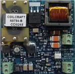
AN-1305 LM5030 Evaluation Board
The AN-1305 is an evaluation board the demonstrates a fully featured push-pull converter utilizing the
LM5030 100V push-pull current mode PWM controller
1
Introduction
The LM5030EVAL evaluation board provides the design engineer with a fully functional push-pull power
converter using the LM5030 PWM controller. The performance of the board is:
• Input range: 36V to 75V
• Output voltage: 3.3V
• Output current: 0 to 10A
• Measured efficiency: 82% (at 48V in, 10A Load Current)
• Board size: 2.4 × 2.4 × 0.5 inches
• Load regulation: ±1.0% (1 - 10A)
• Line regulation: ±0.15% (36 - 75V)
• Shutdown input
• Synchronizing input
The printed circuit board consists of 2 layers of 2 ounce copper on FR4 material, with a total thickness of
0.062 inches. The board is designed for continuous operation at rated load.
2
Theory of Operation
Referring to Figure 10, the LM5030 controller (U1) alternately drives two N channel MOSFETs, which feed
the two halves of the power transformer’s primary (T1). The transformer’s secondary is rectified, and
filtered with an LC filter (L2, C3-5), to provide the output voltage. The feedback path starts with the
LM3411 precision regulator driver (U3) which senses the output voltage, compares it to its internal
reference, and drives an optocoupler (U2) based on the error voltage. The optocoupler provides isolation
in the feedback path, and its open collector output drives the COMP pin on the LM5030, which controls
the pulse width to the MOSFETs. The lower the voltage at the COMP pin, the smaller the MOSFET duty
cycle.
Current in the main transformer’s primary is monitored at the LM5030’s CS pin via a current sense
transformer (T2). The voltage at the CS pin is used for current mode PWM control and current limit
protection.
The output inductor (L2) not only smoothes the output voltage waveform, but also generates an auxiliary
voltage (by means of its secondary winding) to power the Vcc pin on the LM5030. This feature reduces
power dissipation within the IC, thereby increasing reliability.
A Synchronizing input pad (SYNC) is provided on the board to synchronize the circuit’s operating
frequency to an external source. A Shutdown input pad (SD) permits shutting down the circuit’s operation
from an external switch to ground.
All trademarks are the property of their respective owners.
SNVA078A – May 2004 – Revised May 2013
Submit Documentation Feedback
AN-1305 LM5030 Evaluation Board
Copyright © 2004–2013, Texas Instruments Incorporated
1
�Board Layout and Probing
3
www.ti.com
Board Layout and Probing
Figure 1 shows the placement of the significant components which may be probed in evaluating the
circuit’s operation. The following should be kept in mind when using scope or meter probes:
1. The board has two circuit grounds - one associated with the input power, and one associated with the
output power. The grounds are capacitively coupled (C6), but are DC isolated.
2. The main current carrying components (L1, T1, T2, Q1, Q2, D1 and L2) will be hot to the touch at
maximum load current. USE CAUTION. If operating at maximum load current for extended periods, the
use of a fan to provide forced air flow is recommended.
3. Use care when probing the primary side at maximum input voltage. 75 volts is enough to produce
shocks and sparks.
4. At maximum load current (10A), the wire size, and length, used to connect the board’s output to the
load becomes important. Ensure there is not a significant voltage drop in the wires. Note that two
connectors are provided at the output - one for the +3.3V output (J2 Out), and one for the Ground
connection (J3 IGND). It is advisable to make good use of this feature to ensure a low loss connection.
5. The input voltage conector is J1.
4
5
L2
6
D1
C6
3
2
OUT
C3
U3
T1
1
C4
J2
T2
C5
Q1
U2
L1
IGND
GND
IN J1
U1
SYN
C
S
D
J3
Q2
Figure 1. Evaluation Board
2
AN-1305 LM5030 Evaluation Board
SNVA078A – May 2004 – Revised May 2013
Submit Documentation Feedback
Copyright © 2004–2013, Texas Instruments Incorporated
�Board Connections/Start-Up
www.ti.com
4
Board Connections/Start-Up
The input connection to the board from a power supply is made to connector J1. The power supply must
be capable of supplying not only the current during normal operation, but also the inrush current during
start-up. For example, if the load current is set to be 1.0A, the inrush current will be approximately 250 mA
peak. If the load is set to 10A, the inrush current will be approximately 1.7A peak. Once the circuit is on
and operating normally, the current draw from the power supply is a function of both the load current, and
the input voltage, as shown in Figure 2.
The load is connected to the J2 and J3 connectors. Two connectors are provided to accommodate
adequately sized wires. With a load current of 10A, the load connections should use a minimum of 16
gauge wire, preferably larger.
Before start-up, a voltmeter should be connected to the input terminals, and one to the output terminals.
The input current should be monitored with either an ammeter, or a current probe. Upon turning on the
power supply, these three meters should be immediately checked to ensure their readings are nominal.
1.2
INPUT CURRENT (A)
1.0
VIN = 36V
0.8
VIN = 75V
0.6
0.4
0.2
0.0
0
5
10
LOAD CURRENT (A)
Figure 2. Input Current vs Load Current and VIN
SNVA078A – May 2004 – Revised May 2013
Submit Documentation Feedback
AN-1305 LM5030 Evaluation Board
Copyright © 2004–2013, Texas Instruments Incorporated
3
�Performance
5
www.ti.com
Performance
Once the circuit is powered up and operating normally, the output voltage will be regulated to +3.3V, with
the accuracy determined by the accuracy of the LM3411 regulator driver. As the load current is varied
from 1.0 to 10A, the output is regulated to within +/-30 mV (+/- 1.0%). For a given load current, the output
will be regulated to within 5 mV as the input voltage is varied over its range (36 - 75V). The power
conversion efficiency is shown in Figure 3.
100
VIN = 36V
90
80
EFFICIENCY (%)
VIN = 75V
70
60
50
40
30
20
0
2
4
6
8
10
LOAD CURRENT (A)
Figure 3. Efficiency vs Load Current and VIN
6
Waveforms
If the circuit is to be probed, Figure 4 shows some of the significant waveforms for various input/output
combinations. Remember that there are two circuit grounds, and the scope probe grounds must be
connected appropriately.
In the table of Figure 4, t1 and t2 are in microseconds, while Fs is in kHz. Fs is the frequency of the
internal oscillator, which is twice the switching frequency of each MOSFET. All the voltages are in volts
with respect to circuit ground. L2 Output is the regulated output at J2, and typically has less than 10mV of
ripple. The spikes at the rising edges of V4, V5, V7, and V9 are due to the leakage inductance in T1. The
voltage rating of the MOSFETs (Q1, Q2) is determined by the amplitude of these spikes (V4). Their
current rating is determined by the input current shown in Figure 2, plus a ripple component of
approximately 10% in this design.
4
AN-1305 LM5030 Evaluation Board
SNVA078A – May 2004 – Revised May 2013
Submit Documentation Feedback
Copyright © 2004–2013, Texas Instruments Incorporated
�VCC
www.ti.com
V1
Q2 Gate
0V
t1
t2
V1
Q1 Gate
0V
V4
V3
V2
Q2 Drain
tR = 150 ns
0V
V5
V6
T1 (Pin 4)
0V
V8
V7
V9
V10
D1 Output
0V
L2 Output
3.3V
100 mVp-p
VIN
IOUT
t1
t2
Fs
V1
V2
V3
V4
V5
V6
V7
V8
V9
V10
36V
1.0A
2.2µS
5.3µS
266.7
10.5V
36V
48V
10A
1.9µS
5.5µS
270.3
11.5V
48V
72V
90V
10V
6V
-10V
-6V
10V
6V
96V
130V
18V
8V
-18V
-8V
13V
75V
1.0A
1.2µS
6.2µS
270.3
10.5V
75V
8V
150V
200V
20V
13V
-20V
-13V
20V
13V
Figure 4. Representative Waveforms
7
VCC
While the LM5030 internally generates a voltage at VCC (7.7V), the internal regulator is used mainly during
the start-up sequence. Once the load current begins flowing through L2, which is both an inductor for the
output filter and a transformer, a voltage is generated at L2’s secondary which powers the VCC pin. Once
the externally applied voltage exceeds the internal value (7.7V), the internal regulator shuts off, thereby
reducing internal power dissipation in the LM5030. L2 is constructed such that the voltage supplied to VCC
ranges from approximately 10.6V to approximately 11.3V, depending on the load current. See Figure 5.
SNVA078A – May 2004 – Revised May 2013
Submit Documentation Feedback
AN-1305 LM5030 Evaluation Board
Copyright © 2004–2013, Texas Instruments Incorporated
5
�Current Sense
www.ti.com
11.3
11.2
11.1
VCC (V)
11.0
10.9
10.8
10.7
10.6
10.5
0.0
2.0
4.0
6.0
8.0
10.0
LOAD CURRENT (A)
Figure 5. VCC Voltage vs Load Current
8
Current Sense
Monitoring the input current provides a good indication of the circuit’s operation. If an overload condition
should exist at the output (a partial overload or a short circuit), the input current would rise above the
nominal value shown in Figure 2. Transformer T2, in conjunction with D3, R9, R12 and C10, provides a
voltage to pin 8 on the LM5030 (CS) which is representative of the input current flowing through its
primary. The average voltage seen at pin 8 is plotted in Figure 6. If the voltage at the first current sense
comparator exceeds 0.5V, the LM5030 disables its outputs, and the circuit enters a cycle-by-cycle current
limit mode. If the second level threshold (0.625V) is exceeded due to a severe overload and transformer
saturation, the LM5030 will disable its outputs and initiate a softstart sequence. However, the very short
propagation delay of the cycle-by-cycle current limiter (CS1), the design of the CS filter (R9, R12, and
C10), and the conservative design of the output inductor (L2), may prevent the second level current
threshold from being realized on this evaluation board.
AVERAGE VOLTAGE @ CS (V)
0.25
0.20
0.15
0.10
0.05
0.00
0.0
0.2
0.4
0.6
0.8
1.0
INPUT CURRENT (A)
Figure 6. Average Voltage at the CS pin vs Input Current
6
AN-1305 LM5030 Evaluation Board
SNVA078A – May 2004 – Revised May 2013
Submit Documentation Feedback
Copyright © 2004–2013, Texas Instruments Incorporated
�Shutdown
www.ti.com
9
Shutdown
The Shutdown pad (SD) on the board connects to the SoftStart pin on the LM5030 (pin 10), and permits
on/off control of the converter by an external switch. SD should be pulled below 0.45V, with an open
collector or open drain device, to shut down the LM5030 outputs and the VCC regulator. If the voltage at
the SD pad is between 1.0 and 1.5V, a partial-on condition results, which could be disruptive to the
system. Therefore, the voltage at the SD pad should transition quickly between its open circuit voltage
(4.9V) and ground.
10
External Sync
Although the LM5030 includes an internal oscillator, its operating frequency can be synchronized to an
external signal if desired. The external source frequency must be higher than the internal frequency set
with the RT resistor (262kHz with RT = 20K). The sync input pulse width must be between 15 and 150 ns,
and have an amplitude of 1.5 - 3.0V at the Sync pad on the board. The pulses are coupled to the LM5030
through a 100pF capacitor (C16) as specified in the data sheet.
11
Bill Of Materials
Table 1. Bill Of Materials
Item
Part Number
Description
Value
C1
C0805C472K5RAC
Capacitor, Ceramic, KEMET
4700pF, 50V
C2
C0805C103K5RAC
Capacitor, Ceramic, KEMET
0.01µF, 50V
C3
C4532X7S0G686M
Capacitor, Ceramic, TDK
68µF, 4V
T520D337M006AS4350
Capacitor, Tantalum, KEMET
330µF, 6.3V
C6
C4532X7R3A103K
Capacitor, Ceramic, TDK
0.01µF, 1000V
C7
C3216X7R2A104K
Capacitor, Ceramic, TDK
0.1µF, 100V
C8, 9
C4532X7R2A105M
Capacitor, Ceramic, TDK
1µF, 100V
C10
C0805C102K1RAC
Capacitor, Ceramic, KEMET
1000pF, 100V
C11
C1206C223K5RAC
Capacitor, Ceramic, KEMET
0.022µF, 50V
C12
C3216X7R1E105M
Capacitor, Ceramic, TDK
1µF, 25V
C13, 14
C3216COG2J221J
Capacitor, Ceramic, TDK
220pF, 630V
C4, 5
C15
C1206C104K5RAC
Capacitor, Ceramic, KEMET
0.1µF, 50V
C16, 17
C0805C101J1GAC
Capacitor, Ceramic, KEMET
100pF, 100V
C18
C3216X7R1H334K
Capacitor, Ceramic, TDK
0.33µF, 50V
D1
MBRB3030CTL
Diode, Schottky, ON Semi.
30V, 15A
D2 - 5
CMPD2838-NSA
Diode, Signal, Central Semi.
75V, 200mA
L1 (1)
MSS6132-103
Input Choke, Coilcraft
10µH, 1.3A
L2 (1)
A9785-B
Output Choke, Coilcraft
7µH, 15A
R1
CRCW12061R00F
Resistor, 1206 SMD
1.0
R2
CRCW12064990F
Resistor, 1206 SMD
499
CRCW2512101J
Resistor, 2512 SMD
100, 1Ω
R3, 4
(1)
R5
CRCW12064022F
Resistor, 1206 SMD
40.2K
R6, 7, 13
CRCW120610R0F
Resistor, 1206 SMD
10
R8
CRCW12061002F
Resistor, 1206 SMD
10K
R9
CRCW120623R7F
Resistor, 1206 SMD
23.7
R10
CRCW12062002F
Resistor, 1206 SMD
20K
R11
CRCW120649R9F
Resistor, 1206 SMD
49.9
R12
CRCW12063010F
Resistor, 1206 SMD
301
R14
CRCW12061001F
Resistor, 1206 SMD
1.0K
T1 (1)
A9784-B
Power Transformer, Coilcraft
33Ω, 10A
Data sheets for L1, L2, and T1 are available from Coilcraft at http://www.coi1craft.com/prod_pwr.cfm.
SNVA078A – May 2004 – Revised May 2013
Submit Documentation Feedback
AN-1305 LM5030 Evaluation Board
Copyright © 2004–2013, Texas Instruments Incorporated
7
�PCB Layout Diagrams
www.ti.com
Table 1. Bill Of Materials (continued)
Item
Part Number
Description
Value
T2 (2)
P8208T
Current Transformer, Pulse Eng.
100:1, 10A
(3)
U1
(2)
(3)
12
LM5030
PWM Regulator, Texas Instruments
U2
MOCD207M
Opto-Coupler, Fairchild
U3
LM3411
Reference Regulator, Texas
Instruments
3.3V
Q1, 2
SUD19N20-90
FET, N Channel, Vishay
200V, 19A
J1-3
651-1727010
Dual Terminals, Mouser
3 per Assy.
Data sheet for T2 is available from Pulse Engineering at http://www.pulseeng.com/default.cfm.
LM5030 100V Push-Pull Current Mode PWM Controller (SNVS215)
PCB Layout Diagrams
Figure 7. Bottom Layer (viewed from top)
8
AN-1305 LM5030 Evaluation Board
SNVA078A – May 2004 – Revised May 2013
Submit Documentation Feedback
Copyright © 2004–2013, Texas Instruments Incorporated
�PCB Layout Diagrams
www.ti.com
Figure 8. Top Silk Screen
Figure 9. Top Layer
SNVA078A – May 2004 – Revised May 2013
Submit Documentation Feedback
AN-1305 LM5030 Evaluation Board
Copyright © 2004–2013, Texas Instruments Incorporated
9
�Board Schematic
13
www.ti.com
Board Schematic
Figure 10. Board Schematic
10
AN-1305 LM5030 Evaluation Board
SNVA078A – May 2004 – Revised May 2013
Submit Documentation Feedback
Copyright © 2004–2013, Texas Instruments Incorporated
�IMPORTANT NOTICE
Texas Instruments Incorporated and its subsidiaries (TI) reserve the right to make corrections, enhancements, improvements and other
changes to its semiconductor products and services per JESD46, latest issue, and to discontinue any product or service per JESD48, latest
issue. Buyers should obtain the latest relevant information before placing orders and should verify that such information is current and
complete. All semiconductor products (also referred to herein as “components”) are sold subject to TI’s terms and conditions of sale
supplied at the time of order acknowledgment.
TI warrants performance of its components to the specifications applicable at the time of sale, in accordance with the warranty in TI’s terms
and conditions of sale of semiconductor products. Testing and other quality control techniques are used to the extent TI deems necessary
to support this warranty. Except where mandated by applicable law, testing of all parameters of each component is not necessarily
performed.
TI assumes no liability for applications assistance or the design of Buyers’ products. Buyers are responsible for their products and
applications using TI components. To minimize the risks associated with Buyers’ products and applications, Buyers should provide
adequate design and operating safeguards.
TI does not warrant or represent that any license, either express or implied, is granted under any patent right, copyright, mask work right, or
other intellectual property right relating to any combination, machine, or process in which TI components or services are used. Information
published by TI regarding third-party products or services does not constitute a license to use such products or services or a warranty or
endorsement thereof. Use of such information may require a license from a third party under the patents or other intellectual property of the
third party, or a license from TI under the patents or other intellectual property of TI.
Reproduction of significant portions of TI information in TI data books or data sheets is permissible only if reproduction is without alteration
and is accompanied by all associated warranties, conditions, limitations, and notices. TI is not responsible or liable for such altered
documentation. Information of third parties may be subject to additional restrictions.
Resale of TI components or services with statements different from or beyond the parameters stated by TI for that component or service
voids all express and any implied warranties for the associated TI component or service and is an unfair and deceptive business practice.
TI is not responsible or liable for any such statements.
Buyer acknowledges and agrees that it is solely responsible for compliance with all legal, regulatory and safety-related requirements
concerning its products, and any use of TI components in its applications, notwithstanding any applications-related information or support
that may be provided by TI. Buyer represents and agrees that it has all the necessary expertise to create and implement safeguards which
anticipate dangerous consequences of failures, monitor failures and their consequences, lessen the likelihood of failures that might cause
harm and take appropriate remedial actions. Buyer will fully indemnify TI and its representatives against any damages arising out of the use
of any TI components in safety-critical applications.
In some cases, TI components may be promoted specifically to facilitate safety-related applications. With such components, TI’s goal is to
help enable customers to design and create their own end-product solutions that meet applicable functional safety standards and
requirements. Nonetheless, such components are subject to these terms.
No TI components are authorized for use in FDA Class III (or similar life-critical medical equipment) unless authorized officers of the parties
have executed a special agreement specifically governing such use.
Only those TI components which TI has specifically designated as military grade or “enhanced plastic” are designed and intended for use in
military/aerospace applications or environments. Buyer acknowledges and agrees that any military or aerospace use of TI components
which have not been so designated is solely at the Buyer's risk, and that Buyer is solely responsible for compliance with all legal and
regulatory requirements in connection with such use.
TI has specifically designated certain components as meeting ISO/TS16949 requirements, mainly for automotive use. In any case of use of
non-designated products, TI will not be responsible for any failure to meet ISO/TS16949.
Products
Applications
Audio
www.ti.com/audio
Automotive and Transportation
www.ti.com/automotive
Amplifiers
amplifier.ti.com
Communications and Telecom
www.ti.com/communications
Data Converters
dataconverter.ti.com
Computers and Peripherals
www.ti.com/computers
DLP® Products
www.dlp.com
Consumer Electronics
www.ti.com/consumer-apps
DSP
dsp.ti.com
Energy and Lighting
www.ti.com/energy
Clocks and Timers
www.ti.com/clocks
Industrial
www.ti.com/industrial
Interface
interface.ti.com
Medical
www.ti.com/medical
Logic
logic.ti.com
Security
www.ti.com/security
Power Mgmt
power.ti.com
Space, Avionics and Defense
www.ti.com/space-avionics-defense
Microcontrollers
microcontroller.ti.com
Video and Imaging
www.ti.com/video
RFID
www.ti-rfid.com
OMAP Applications Processors
www.ti.com/omap
TI E2E Community
e2e.ti.com
Wireless Connectivity
www.ti.com/wirelessconnectivity
Mailing Address: Texas Instruments, Post Office Box 655303, Dallas, Texas 75265
Copyright © 2013, Texas Instruments Incorporated
�


 工商网监
湘ICP备2023018690号
工商网监
湘ICP备2023018690号
