User's Guide
SLVUAA1 – September 2014
Evaluation Module for LM5069EVM-627 with Surge
Stopper and Reverse Voltage Protection
This user’s guide describes the evaluation module (EVM) for the LM5069. The LM5069 is a positive high
voltage hotswap/inrush current controller with power limiting.
1
2
3
4
5
6
7
8
9
Contents
Introduction ................................................................................................................... 2
1.1
Features .............................................................................................................. 2
1.2
Applications .......................................................................................................... 2
Board Description ............................................................................................................ 3
Theory of Operation ......................................................................................................... 3
Board Connection/Setup and Probe Cautions ........................................................................... 4
Circuit Parameter Changes ................................................................................................. 5
5.1
Current Limit ......................................................................................................... 5
5.2
Power Limit .......................................................................................................... 5
5.3
Insertion Time ....................................................................................................... 5
5.4
Fault Detection and Restart ....................................................................................... 5
5.5
UVLO/OVLO Input Voltage Thresholds .......................................................................... 6
5.6
Surge Clamping ..................................................................................................... 9
5.7
Shutdown ............................................................................................................ 9
5.8
Power Good Output ............................................................................................... 10
5.9
Reverse Hookup Protection ...................................................................................... 10
Performance Characteristics Plots ....................................................................................... 10
6.1
Reverse Polarity Input ............................................................................................ 10
6.2
Insertion Time Delay .............................................................................................. 11
6.3
Fault Timeout ...................................................................................................... 11
6.4
Restart Timing ..................................................................................................... 12
6.5
Turn-on Sequence with No Load Current ...................................................................... 12
6.6
Turn-on Sequence with 1-A Load Current ..................................................................... 13
6.7
Output Shutdown Using UVLO Pin ............................................................................. 13
6.8
Input Surge ......................................................................................................... 14
6.9
Inrush Current ..................................................................................................... 15
Schematic ................................................................................................................... 17
PCB Layout ................................................................................................................. 18
Bill of Materials (BOM) ..................................................................................................... 20
List of Figures
1
Power Up Using Power Limit and Current Limit ......................................................................... 4
2
Fault Timeout and Restart Sequence ..................................................................................... 6
3
UVLO, OVLO Inputs (Option A)............................................................................................ 7
4
UVLO, OVLO Inputs (Option B)............................................................................................ 8
5
Minimum UVLO Threshold, Adjustable OVLO ........................................................................... 9
6
Reverse Polarity Input ..................................................................................................... 10
7
Insertion Timer Delay ...................................................................................................... 11
8
Fault Timeout ............................................................................................................... 11
9
Restart Timing .............................................................................................................. 12
SLVUAA1 – September 2014
Submit Documentation Feedback
Evaluation Module for LM5069EVM-627 with Surge Stopper and Reverse
Voltage Protection
Copyright © 2014, Texas Instruments Incorporated
1
�Introduction
www.ti.com
10
Turn-on Sequence with No Load Current ............................................................................... 12
11
Turn-on Sequence with 1-A Load Current .............................................................................. 13
12
Output Shutdown Using UVLO Pin ...................................................................................... 13
13
Output Shutdown Using UVLO Pin ...................................................................................... 14
14
Input Surge (Not Clamped)
14
15
Input Surge (Clamped)
15
16
17
18
19
20
21
...............................................................................................
....................................................................................................
Inrush Current with 2550-µF Output Capacitor .........................................................................
Inrush Current with 4900-µF Output Capacitor .........................................................................
LM5069EVM-627 Schematic .............................................................................................
Top Side Placement .......................................................................................................
Top Layer....................................................................................................................
Bottom Layer ................................................................................................................
15
16
17
18
18
19
List of Tables
1
1
Bill of Materials
.............................................................................................................
20
Introduction
The LM5069EVM-627 provides the design engineer with a fully-functional hotswap controller board
designed for surge clamping, reverse voltage protection and reverse current protect. This board contains
an LM5069-2, the auto restart version of this IC. This user’s guide describes the various functions of the
board: how to test and evaluate it, and how to change the components for a specific application. For more
information, view the LM5069 Positive High Voltage Hot Swap / Inrush Current Controller with Power
Limiting (SNVS452) data sheet.
1.1
Features
•
•
•
•
•
•
1.2
Applications
•
•
•
2
General board specifications include:
– Input voltage range: –40 V to +38 V maximum
– Output voltage clamped: +32 V maximum
– Current limit: 2.5 A, ±10%
– Q1 power limit: 30 W
– UVLO thresholds: 16 V, ±4% and 14 V, ±3%
– OVLO thresholds: 36 V, ±2% and 34 V, ±3%
– Insertion delay: 410 ms
– Fault timeout period: 26 ms
– Restart time: 5.3 seconds
– Size: 4.0" x 1.8"
Reverse connection protection with diode D1
Input surge clamping with TVS diode Z1
Reverse current blocking from load with FET Q2
FET SOA protection with resistor R9
Optional FET Q3 for small input surge
Automotive
24-V industrial systems
General hot plug
Evaluation Module for LM5069EVM-627 with Surge Stopper and Reverse
Voltage Protection
Copyright © 2014, Texas Instruments Incorporated
SLVUAA1 – September 2014
Submit Documentation Feedback
�Board Description
www.ti.com
2
Board Description
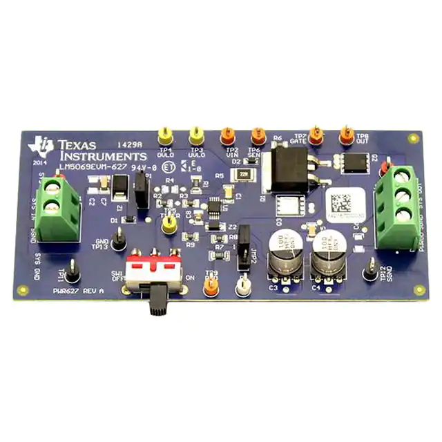
The schematic of LM5069EVM-627 is shown in Figure 18. Input power is applied at J1 while J2 provides
the output connection to the load. Slide switch SW1 provides a means to ENABLE and shutdown the
hotswap circuit with UVLO protection. Capacitors C3 and C4 (100 µF/50 V, Alum Electrolytic capacitor)
represent capacitance which is typically present on the input of the load circuit and are present on this
evaluation board so the turn-on characteristics of the LM5069 may be tested without having to connect a
load.
The LM5069EVM-627 is supplied with pins 2–3 connected on JMP1, and pins 1–2 connected on JMP2.
3
Theory of Operation
The LM5069 provides intelligent control of the power supply connections of a load which is to be
connected to a live power source. The three primary functions of this LM5069EVM-627 are reverse input
voltage hookup, surge clamping and in-rush current limiting during turn-on, and reverse load current
protection when pull out from power source. Additional functions include undervoltage lock-out (UVLO)
and overvoltage lock-out (OVLO) to ensure the system input voltage is supplied to the load within a
defined range, monitoring of the load current for faults during normal operation, power limiting in the series
pass FET (Q1) during turn-on, and a power good logic output (PGD) to indicate the circuit status.
Upon applying the input voltage to the LM5069EVM-627 (for example, SW1 is switched on), Q1 is initially
held off for the insertion delay (≈410 ms) to allow ringing and transients at the input to subside. At the end
of the insertion delay, if the input voltage at VIN is between the UVLO and OVLO thresholds, Q1 is turned
on in a controlled manner to limit the in-rush current, Q2 is also turned on controlled by GATE. If the inrush current were not limited during turn-on, the current would be very high as the load capacitors (C3,
C4) charge up, limited only by the surge current capability of the voltage source, and the wiring resistance
(a few milliohms). That very high current could damage the edge connector, PC board traces, and
possibly the load capacitors receiving the high current. Additionally, the dV/dt at the load’s input is
controlled to reduce possible EMI problems.
The LM5069EVM-627 protects from reverse connection with diode D1. When a reverse power source is
connected, there will be no voltage at each pin of LM5069, as this diode can hold the reverse voltage in a
range, and prevent destroying the IC.
The LM5069EVM-627 limits in-rush current to a safe level using a two-step process. In the first portion of
the turn-on cycle, when the voltage differential across Q1 is highest, Q1’s power dissipation is limited to a
peak of 30 W by monitoring its drain current (the voltage across R5) and its drain-to-source voltage. Their
product is maintained constant by controlling the drain current as the drain-to-source voltage decreases
(as the output voltage increases). This is shown in the constant power portion of Figure 1 where the drain
current is increasing to ILIM. When the drain current reaches the current limit threshold (2.5 A), it is then
maintained constant as the output voltage continues to increase. When the output voltage reaches the
input voltage (VDS decreases to near zero), the drain current then reduces to a value determined by the
load. Q1’s gate-to-source voltage then increases to ≈12 V above the OUT voltage. The circuit is now in
normal operation mode.
Monitoring of the load current for faults during normal operation is accomplished using the current limit
circuit described previously. If the load current increases to 2.5 A (55 mV across R5), Q1’s gate is
controlled to prevent the current from increasing further. When current limiting takes effect, the fault timer
limits the duration of the fault. At the end of the fault timeout period (≈26 ms) Q1 is shut off, denying
current to the load. The LM5069-2 then initiates a restart every 5.3 seconds. The restart consists of
turning on Q1 and monitoring the load current to determine if the fault is still present. After the fault is
removed, the circuit powers up to normal operation at the next restart.
In a sudden overload condition (the output is shorted to ground), it is possible the current could increase
faster than the response time of the current limit circuit. In this case, the circuit breaker sensor shuts off
Q1’s gate rapidly when the voltage across R5 reaches ≈105 mV. When the current reduces to the current
limit threshold, the current limit circuitry then takes over.
The PGD logic level output is low during turn-on, and switches high when the output voltage at OUT has
increased to within 1.25 V of the input voltage, signifying the turn-on procedure is essentially complete. If
the OUT voltage decreases more than 2.5 V below VIN due to a fault, PGD switches low. The high level
voltage at PGD can be any appropriate voltage up to +80 V, and can be higher or lower than the voltages
at VIN and OUT.
SLVUAA1 – September 2014
Submit Documentation Feedback
Evaluation Module for LM5069EVM-627 with Surge Stopper and Reverse
Voltage Protection
Copyright © 2014, Texas Instruments Incorporated
3
�Board Connection/Setup and Probe Cautions
www.ti.com
The UVLO and OVLO thresholds are set by resistors R1–R3. The UVLO and OVLO thresholds are
reached when the voltage at the UVLO and OVLO pins each reach 2.5 V to GND (not SGND),
respectively. The internal 21-μA current sources provide hysteresis for each of the thresholds.
VIN
VDS
Drain Current
ILIM
2.5 A
0
Constant
Power
12 V
Gate-to-Source Voltage
VGS,P
VTH
Turn-on
Normal
Operation
0
Figure 1. Power Up Using Power Limit and Current Limit
4
Board Connection/Setup and Probe Cautions
The input voltage source is connected to the J1 connector, and the load is connected to the J2 connector
at the OUT and GND terminals. Use twisted wires. A voltmeter should be connected to the input terminals
and one to the output terminals. The input current can be monitored with an ammeter or current probe. To
monitor the status of the PGD output, connect a voltmeter from PGOOD to GND on the J2 terminal block.
Put the slide switch in the ON position.
Increase the input voltage gradually. The input current should remain less than 2 mA until the upper UVLO
threshold is reached (≈16 V). When the threshold is reached, Q1 and Q2 are turned on as described in
Section 3. If viewed on an oscilloscope, the input current increases as shown in Figure 1 before settling at
the value defined by the load. The turn-on timing depends on the input voltage, power limit setting, current
limit setting, and the final load current, and is between ≊3.0 ms with no load current, and ≊7 ms with a 1-A
load current, with VIN = 24 V. See Figure 1, Figure 10, and Figure 11.
The following should be kept in mind when the board is powered:
1. High voltage, equal to system input VSYSIN, is present on C3, C4, Q1, Q2 and various points within
the circuit. Use caution when probing the circuit to prevent injury, as well as possible damage to the
circuit.
2. At maximum load current (2.5 A), the wire size and length used to connect the power source and the
load become important. The wires connecting this evaluation board to the power source should be
twisted together to minimize inductance in those leads. The same applies for the wires connecting this
board to the load. This recommendation is made in order to minimize high voltage transients from
occurring when the load current is shut off.
4
Evaluation Module for LM5069EVM-627 with Surge Stopper and Reverse
Voltage Protection
Copyright © 2014, Texas Instruments Incorporated
SLVUAA1 – September 2014
Submit Documentation Feedback
�Circuit Parameter Changes
www.ti.com
5
Circuit Parameter Changes
5.1
Current Limit
The current limit threshold is set by R5 according to Equation 1:
55 mV 55 mV
ILIM =
=
RS
R5
(1)
If the load current increases such that the voltage across R5 reaches 55 mV, the LM5069 then modulates
Q1’s gate to limit the current to that level. This evaluation board is supplied with a 22-mΩ resistor for R5,
resulting in a current limit of 2.5 A. To change the current limit threshold, replace R5 with a resistor of the
required value and power capability.
For proper operation, the RS resistor value should be no larger than 100 mΩ.
5.2
Power Limit
The maximum power dissipated in Q1 during turn-on, or due to a fault, is limited by R9 and R5 according
to Equation 2:
R9
RPWR
PFET,LIM =
=
5
1.25 ´ 10 ´ RS 1.25 ´ 105 ´ R5
(2)
With the components supplied on the evaluation board, PFET(LIM) = 30 W. During turn-on, when the
voltage across Q1 is high, its gate is modulated to limit its drain current so the power dissipated in Q1
does not exceed 30 W. As the drain-to-source voltage decreases, the drain current increases, maintaining
the power dissipation constant. When the drain current reaches the current limit threshold set by R5 (2.5
A), the current is then maintained constant until the output voltage reaches its final value. The current then
decreases to a value determined by the load, see Figure 10, and Figure 11.
Each time Q1 is subjected to the maximum power limit conditions it is internally stressed for a few
milliseconds. For this reason, keep in mind that the power limit threshold must be set lower than the limit
indicated by the FET’s SOA chart. In this evaluation board, the power limit threshold is set at 30 W,
compared to ≈80 W limit indicated in the Vishay SUM50N06-16L data sheet. The FET manufacturer
should be contacted for more information on this subject.
5.3
Insertion Time
The insertion time starts when the input voltage at VIN reaches 7.6 V, and its duration equals:
4V
tinsertion = CT ´
= C8 ´ 7.24 ´ 105
5.5 mA
(3)
During the insertion time, Q1 is held off regardless of the voltage at VIN. This delay allows ringing and
transients at VIN to subside before the input voltage is applied to the load via Q1. The insertion time on
this evaluation board is ≈400 ms (see Figure 7).
5.4
Fault Detection and Restart
If the load current increases to the fault level (the current limit threshold, 2.5 A), an internal current source
charges the timing capacitor C8 at the TIMER pin. When the voltage at the TIMER pin reaches 4.0 V, the
fault timeout period is complete, and the LM5069 shuts off Q1. The restart sequence then begins,
consisting of seven cycles at the TIMER pin between 4.0 V and 1.25 V, as shown in Figure 2. When the
voltage at the TIMER pin reaches 0.3 V during the eighth high-to-low ramp, Q1 is turned on. If the fault is
still present, the fault timeout period and the restart sequence repeat.
SLVUAA1 – September 2014
Submit Documentation Feedback
Evaluation Module for LM5069EVM-627 with Surge Stopper and Reverse
Voltage Protection
Copyright © 2014, Texas Instruments Incorporated
5
�Circuit Parameter Changes
Load
Current
www.ti.com
Fault
Detection
ILIMT
GATE
Voltage
4V
TIMER
1.25 V
Voltage
Fault Timeout
Detection
1
2
3
7
8
0.3 V
tRESTART
Figure 2. Fault Timeout and Restart Sequence
The fault timeout period and the restart timing are determined by the TIMER capacitor C8 according to
Equation 4 and Equation 5:
4V
t fault = CT ´
= C8 ´ 4.7 ´ 104
85 mA
(4)
é 7 ´ 2.75 V 7 ´ 2.75 V 3.7 V ù
6
+
+
trestart = CT ´ ê
ú = C8 ´ 9.4 ´ 10
m
m
m
2.5
A
85
A
2.5
A
ë
û
(5)
The waveform at the TIMER pin can be monitored at the test pad located between C8 and R9. In this
evaluation board, the fault timeout period is ≈26 ms, and the restart time is ≈5.3 seconds (see Figure 8
and Figure 9).
5.5
UVLO/OVLO Input Voltage Thresholds
As supplied, the input voltage UVLO thresholds on this evaluation board are approximately 16 V
increasing, and 14 V decreasing. The OVLO thresholds are approximately 36 V increasing, and 34 V
decreasing. The four thresholds are determined by resistors R1–R4. The threshold voltage at each pin is
2.5 V to GND (not SGND), and internal 21-μA current sources provide hysteresis for each threshold. See
the device data sheet for more details.
Option A: This evaluation board is supplied with the jumper at JMP1 on pins 2–3, resulting in the
configuration shown in Figure 3.
6
Evaluation Module for LM5069EVM-627 with Surge Stopper and Reverse
Voltage Protection
Copyright © 2014, Texas Instruments Incorporated
SLVUAA1 – September 2014
Submit Documentation Feedback
�Circuit Parameter Changes
www.ti.com
SYSIN
VIN
2
R1
95.3 kQ
VIN
3
UVLO
R2
14.7 kQ
LM5069
4
OVLO
R3
8.45 kQ
D1
Note: R4 is open
Figure 3. UVLO, OVLO Inputs (Option A)
To change the thresholds in this configuration, resistors R1–R3 are calculated using the following
procedure:
• Choose the upper UVLO threshold (VUVH), and the lower UVLO threshold (VUVL)
• Choose the upper OVLO threshold (VOVH)
The lower OVLO threshold (VOVL) cannot be chosen in advance in this case, but is determined after the
values for R1–R3 are determined. If VOVL must be accurately defined in addition to the other three
thresholds, see Option B following Equation 7.
The resistors are calculated as follows:
(VUVH - VF ) - (VUVL - VF )
R1 =
21 mA
R3 =
R2 =
2.5 V ´ R1 ´ (VUVL - VF )
(VOVH - VF )´ (VUVL - VF - 2.5 V )
2.5 V ´ R1
- R3
VUVL - VF - 2.5 V
VF = VF,D1
(6)
NOTE: VF is the forward voltage of diode D1.
The lower OVLO threshold is calculated from:
é
æ 2.5V
öù
- 21 mA ÷ ú + 2.5 V + VF
VOVL = ê(R1 + R2 )´ ç
è R3
ø ûú
ëê
SLVUAA1 – September 2014
Submit Documentation Feedback
Evaluation Module for LM5069EVM-627 with Surge Stopper and Reverse
Voltage Protection
Copyright © 2014, Texas Instruments Incorporated
(7)
7
�Circuit Parameter Changes
www.ti.com
Option B: If all four thresholds must be determined accurately, move the jumper at JMP1 to pins 1–2, and
add R4, resulting in the configuration shown in Figure 4:
SYSIN
VIN
R1
95.3 kQ
R2
95.3 kQ
R4
23.2 kQ
VIN
3
UVLO
LM5069
4
OVLO
R3
7.32 kQ
D1
Figure 4. UVLO, OVLO Inputs (Option B)
The four resistor values are calculated as follows:
Choose the upper and lower UVLO thresholds (VUVH) and (VUVL):
R1 =
(VUVH - VF ) - (VUVL - VF )
21 mA
(8)
2.5 V ´ R1
R4 =
VUVL - VF - 2.5 V
(9)
Choose the upper and lower OVLO threshold (VOVH) and (VOVL):
(VUVH - VF ) - (VUVL - VF )
R2 =
21 mA
2.5 V ´ R2
R3 =
VOVH - VF - 2.5 V
(10)
CAUTION
The absolute maximum rating for the OVLO pin is 7 V. Do not let the voltage on
OVLO exceed 7 V when VIN is at its maximum value. The absolute maximum
rating for the UVLO pin is 100 V.
8
Evaluation Module for LM5069EVM-627 with Surge Stopper and Reverse
Voltage Protection
Copyright © 2014, Texas Instruments Incorporated
SLVUAA1 – September 2014
Submit Documentation Feedback
�Circuit Parameter Changes
www.ti.com
Option C: The minimum UVLO level is obtained by positioning the jumper at JMP1 on pins 1–2, and
leaving R4 open, resulting in the configuration shown in Figure 5. Q1 is switched on when the voltage at
VIN reaches the POREN threshold (≈8.4 V). The OVLO thresholds are set by R2 and R3, and their values
are calculated using the procedure in Option B. The value for R1 is not critical, and can be as supplied.
Please adhere to the previous CAUTION.
SYSIN
VIN
2
R1
VIN
3
R2
UVLO
LM5069
4
OVLO
R3
D1
Figure 5. Minimum UVLO Threshold, Adjustable OVLO
Option D: The OVLO function can be disabled by removing the jumper from JMP1. The UVLO thresholds
are set by R1 and R4 using the procedure in Option B or C.
5.6
Surge Clamping
Surge clamping is performed by the FET, Q1 (see Figure 18), which will clamp any input voltages that rise
above the level programmed by Z2. As input voltage increases during a surge event, the output voltage
will also increase and the internal charge pump will try to keep VGATE 12 V above VOUT. Because of Z2,
VGATE cannot rise above VZ_Z2; therefore, VOUT cannot rise above (VZ-Z2 – VTHRESHOLD_Q1).
For a different surge clamp voltage, use the following equation to select an alternate Zener Diode;
VZENER = VLOAD_MAX_SURGE + VTHRESHOLD_Q1
(11)
NOTE: If there is a resistive path < 1 MΩ from VIN (LM5069 pin 2) to GND (LM5069 pin 5) then D2
and R6 are not required. OV, UV programming resistors often provide this resistive path. D2
and R6 are intended to provide a weak gate pin pull down during reverse hookup conditions
in cases where there is no external pull down.
5.7
Shutdown
With the circuit in normal operation, the LM5069 can be shut down by grounding the UVLO pin. Slide
switch SW1, left bottom side of the board, can be used for this purpose. See Figure 12.
SLVUAA1 – September 2014
Submit Documentation Feedback
Evaluation Module for LM5069EVM-627 with Surge Stopper and Reverse
Voltage Protection
Copyright © 2014, Texas Instruments Incorporated
9
�Circuit Parameter Changes
5.8
www.ti.com
Power Good Output
The PGOOD logic output provides an indication of the circuit’s condition. This output is high when the
circuit is in normal operation – the OUT voltage is within 1.25 V of the input. PGOOD is low when the
circuit is shutdown, either intentionally or due to a fault. PGOOD is also high when VIN is less than 5 V.
As the output voltage will be clamped at 32 V, the PGOOD is low when input voltage exceeds 33.5 V.
This EVB is supplied with pins 1–2 connected on JMP2, powering the PGD pin from the output voltage
through a 100-kΩ pull-up resistor. To change the high-level PGOOD voltage, move the jumper on JMP2 to
pins 2–3, and supply the appropriate pull-up voltage to terminal P1 (located next to JMP2). If the UVLO
pin is taken low to disable the LM5069, PGOOD switches low within 10 μs without waiting for the OUT
voltage to fall, see Figure 13.
If a delay at the PGOOD output is desired, a resistor and capacitor can be added at positions R8 and C6.
5.9
Reverse Hookup Protection
When power feeds are incorrectly connected and polarity to the EVM is reversed, a simple low-power
diode (D1) between supply GND and LM5069 GND protects the LM5069 by keeping it off and without
power.
To prevent current from flowing through the body diode of Q1 during reverse supply connection, a second
FET, (Q2), is put in series with Q1. Q1 drain and Q2 Drain connected, creating a back to back FET
configuration.
When VIN < UVLM5069, the gate pin is internally pulled to GND, keeping Q1 and Q2 off.
6
Performance Characteristics Plots
6.1
Reverse Polarity Input
Figure 6. Reverse Polarity Input
Horizontal resolution: 40 ms/div
Channel 1: GATE, 50 V/div
Channel 2: SYS IN, 20 V/div
10
Channel 3: SYS OUT, 20 V/div
Channel 4: IIN, 1 A/div
SYS VIN = –40 V
Evaluation Module for LM5069EVM-627 with Surge Stopper and Reverse
Voltage Protection
Copyright © 2014, Texas Instruments Incorporated
SLVUAA1 – September 2014
Submit Documentation Feedback
�Performance Characteristics Plots
www.ti.com
6.2
Insertion Time Delay
Figure 7. Insertion Timer Delay
Horizontal resolution: 100 ms/div
Channel 1: SYS IN, 20 V/div
Channel 2: TIMER, 5 V/div
6.3
Channel 3: SYS OUT, 10 V/div
CT = 0.56 µF
SYS IN = 24 V
Fault Timeout
Figure 8. Fault Timeout
Horizontal resolution: 100 ms/div
Channel 1: GATE, 20 V/div
Channel 2: TIMER, 2 V/div
Channel 3: IIN, 1 V/div
SLVUAA1 – September 2014
Submit Documentation Feedback
Channel 4: SYS OUT, 10 V/div
CT = 0.56 µF
SYS IN = 24 V
Evaluation Module for LM5069EVM-627 with Surge Stopper and Reverse
Voltage Protection
Copyright © 2014, Texas Instruments Incorporated
11
�Performance Characteristics Plots
6.4
www.ti.com
Restart Timing
Figure 9. Restart Timing
Horizontal resolution: 1.0 s/div
Channel 1: GATE, 20 V/div
Channel 2: TIMER, 2 V/div
Channel 3: IIN, 1 A/div
6.5
Channel 4: SYS OUT, 10 V/div
CT = 0.56 µF
SYS IN = 24 V
Turn-on Sequence with No Load Current
Figure 10. Turn-on Sequence with No Load Current
Horizontal resolution: 1.0 ms/div
Channel 1: GATE, 20 V/div
Channel 2: PGD, 20 V/div
12
Channel 3: IIN, 1 A/div
Channel 4: SYS OUT, 10 V/div
SYS IN = 24 V
Evaluation Module for LM5069EVM-627 with Surge Stopper and Reverse
Voltage Protection
Copyright © 2014, Texas Instruments Incorporated
SLVUAA1 – September 2014
Submit Documentation Feedback
�Performance Characteristics Plots
www.ti.com
6.6
Turn-on Sequence with 1-A Load Current
Figure 11. Turn-on Sequence with 1-A Load Current
Horizontal resolution: 2.0 ms/div
Channel 1: GATE, 20 V/div
Channel 2: PGD, 20 V/div
6.7
Channel 3: IIN, 1 A/div
Channel 4: SYS OUT, 10 V/div
SYS IN = 24 V
Output Shutdown Using UVLO Pin
Figure 12. Output Shutdown Using UVLO Pin
Horizontal resolution: 4.0 ms/div
Channel 1: GATE, 20 V/div
Channel 2: UVLO, 5 V/div
SLVUAA1 – September 2014
Submit Documentation Feedback
Channel 3: SYS OUT, 10 V/div
Channel 4: IOUT, 1 A/div
SYS IN = 24 V
Evaluation Module for LM5069EVM-627 with Surge Stopper and Reverse
Voltage Protection
Copyright © 2014, Texas Instruments Incorporated
13
�Performance Characteristics Plots
www.ti.com
Figure 13. Output Shutdown Using UVLO Pin
Horizontal resolution: 10 µs/div
Channel 1: PGD, 20 V/div
Channel 2: SYS OUT, 10 V/div
6.8
Channel 3: UVLO, 2 V/div
SYS IN = 24 V
Input Surge
Figure 14. Input Surge (Not Clamped)
Horizontal resolution: 400 ms/div
Channel 1: PGD, 20 V/div
Channel 2: SYS OUT, 20 V/div
14
Channel 3: SYS IN, 20 V/div
Channel 4: IIN, 1 A/div
Evaluation Module for LM5069EVM-627 with Surge Stopper and Reverse
Voltage Protection
Copyright © 2014, Texas Instruments Incorporated
SLVUAA1 – September 2014
Submit Documentation Feedback
�Performance Characteristics Plots
www.ti.com
Figure 15. Input Surge (Clamped)
Horizontal resolution: 400 ms/div
Channel 1: PGD, 20 V/div
Channel 2: SYS OUT, 20 V/div
6.9
Channel 3: SYS IN, 20 V/div
Channel 4: IIN, 1 A/div
Inrush Current
Figure 16. Inrush Current with 2550-µF Output Capacitor
Horizontal resolution: 400 ms/div
Channel 1: SYS IN, 20 V/div
Channel 2: GATE, 20 V/div
Channel 3: SYS OUT, 10 V/div
SLVUAA1 – September 2014
Submit Documentation Feedback
Channel 4: IOUT, 1 A/div
SYS IN = 16 V
Output Capacitor: 470 µF × 5 + 100 µF × 2 = 2550 µF
Load: 32-Ω resistor
Evaluation Module for LM5069EVM-627 with Surge Stopper and Reverse
Voltage Protection
Copyright © 2014, Texas Instruments Incorporated
15
�Performance Characteristics Plots
www.ti.com
Figure 17. Inrush Current with 4900-µF Output Capacitor
Horizontal resolution: 1 s/div
Channel 1: SYS IN, 20 V/div
Channel 2: GATE, 20 V/div
Channel 3: SYS OUT, 10 V/div
16
Channel 4: IOUT, 1 A/div
SYS IN = 16 V
Output Capacitor: 470 µF × 10 + 100 µF × 2 = 4900 µF
Load: 900-Ω resistor
Evaluation Module for LM5069EVM-627 with Surge Stopper and Reverse
Voltage Protection
Copyright © 2014, Texas Instruments Incorporated
SLVUAA1 – September 2014
Submit Documentation Feedback
�Schematic
www.ti.com
7
Schematic
The schematic for this EVM is shown in Figure 18.
Q3
CSD18534Q5A
60V
1,2,3
7,8
5,6, DNP
VIN: 24 +/- 6VDC
Optional
Q1
SUM50N06-16L-E3
60V
R5
SIN
DNPC2
1µF
SYS GND
TP6
SEN
TP8
OUT
Z1
SMBJ30CA-13-F
30V
TP11
SYS GND
D2
BAV20WS-TP
150V
TP10
SYS OUT
J2
SOUT
1,2,3
0.022
C7
0.1µF
Q2
CSD18537NQ5A
60V
3
2
1
7,8
5,6,
C3
100µF
C5
0.1µF
4
J1
SYS IN
TP2
VIN
TP1
SYS IN
SYS OUT
SYS GND
PGD
C4
100µF
R6
1.00Meg
SGND
SGND
SGND
1
2
3
JMP1
C1
R1
95.3k
5
4
1
GND
2
2
3
R4
DNP
23.2k
3
4
SW1
1101M2S4AQE2
7
TP4
OVLO
UVLO
OUT
OVLO
GATE
TIMER
SEN
PWR
GND
TP5
TIMER
SGND
SYS GND
TP12
R8
0
8
R7
100k
9
POWERGOOD
DNPC6
1µF
10
GND
1
5
Z2
BZT52C33-7-F
33V
LM5069MM-2/NOPB
P1
JMP2
GND
C8
0.56µF
R9
82.5k
D1
R3
8.45k
GND
PGD
1
2
3
R2
14.7k
6
VIN
SGND
TP9
PGD
U1
TP3
UVLO
SGND
GND
TP7
GATE
1000pF
TP13
GND
GND
GND
BAV20WS-TP
150V
GND
SGND
Figure 18. LM5069EVM-627 Schematic
SLVUAA1 – September 2014
Submit Documentation Feedback
Evaluation Module for LM5069EVM-627 with Surge Stopper and Reverse
Voltage Protection
Copyright © 2014, Texas Instruments Incorporated
17
�PCB Layout
8
www.ti.com
PCB Layout
Figure 19 through Figure 21 illustrate the PCB layouts.
Figure 19. Top Side Placement
Figure 20. Top Layer
18
Evaluation Module for LM5069EVM-627 with Surge Stopper and Reverse
Voltage Protection
Copyright © 2014, Texas Instruments Incorporated
SLVUAA1 – September 2014
Submit Documentation Feedback
�PCB Layout
www.ti.com
Figure 21. Bottom Layer
SLVUAA1 – September 2014
Submit Documentation Feedback
Evaluation Module for LM5069EVM-627 with Surge Stopper and Reverse
Voltage Protection
Copyright © 2014, Texas Instruments Incorporated
19
�Bill of Materials (BOM)
9
www.ti.com
Bill of Materials (BOM)
Table 1 lists the BOM for this EVM.
Table 1. Bill of Materials
Designator
Quantity
!PCB
1
PartNumber
Manufacturer
PWR627
C1
1
1000pF
CAP, CERM, 1000pF, 50V, +/-10%, X7R, 1206
Any
1206
12065C102KAT2A
C3, C4
2
100uF
AVX
CAP, AL, 100uF, 50V, +/-20%, 0.34 ohm, SMD
SMT Radial F
EEE-FK1H101P
C5
1
Panasonic
0.1uF
CAP, CERM, 0.1uF, 50V, +/-10%, X7R, 1206
1206
12065C104KAT2A
C7
AVX
1
0.1uF
CAP, CERM, 0.1uF, 100V, +/-20%, X7R, 1206
1206
C3216X7R2A104M
TDK
C8
1
0.56uF
CAP, CERM, 0.56uF, 25V, +/-10%, X7R, 0805
0805
C0805C564K3RACTU
Kemet
D1, D2
2
150V
Diode, P-N, 150V, 0.2A, SOD-323
SOD-323
BAV20WS-TP
Micro Commercial Components
FID1, FID2, FID3
3
Fiducial mark. There is nothing to buy or mount.
Fiducial
N/A
N/A
H1, H2, H3, H4
4
Bumpon, Cylindrical, 0.312 X 0.200, Black
Black Bumpon
SJ61A1
3M
J1
1
Conn Term Block, 2POS, 5.08mm, TH
2POS Terminal Block
1715721
Phoenix Contact
J2
1
TERM BLOCK 3POS 5.08MM, TH
15.24x13.8x9.8mm
1715734
Phoenix Contact
JMP1, JMP2
2
1x3
Header, 100mil, 3x1, Gold, TH
PBC03SAAN
PBC03SAAN
Sullins Connector Solutions
P1
1
White
Test Point, Multipurpose, White, TH
White Multipurpose Testpoint
5012
Keystone
Q1
1
60V
MOSFET, N-CH, 60V, 50A, DDPAK
DDPAK
SUM50N06-16L-E3
Vishay-Siliconix
Q2
1
60V
MOSFET, N-CH, 60V, 50A, SON 5x6mm
SON 5x6mm
CSD18537NQ5A
Texas Instruments
R1
1
95.3k
RES, 95.3k ohm, 1%, 0.25W, 1206
1206
CRCW120695K3FKEA
Vishay-Dale
R2
1
14.7k
RES, 14.7k ohm, 1%, 0.125W, 0805
0805
CRCW080514K7FKEA
Vishay-Dale
R3
1
8.45k
RES, 8.45k ohm, 1%, 0.125W, 0805
0805
CRCW08058K45FKEA
Vishay-Dale
R5
1
0.022
RES, 0.022 ohm, 1%, 0.5W, 1812
1812
ERJ-L12KF22MU
Panasonic
R6
1
1.00Meg
RES, 1.00Meg ohm, 1%, 0.125W, 0805
0805
CRCW08051M00FKEA
Vishay-Dale
R7
1
100k
RES, 100k ohm, 1%, 0.25W, 1206
1206
CRCW1206100KFKEA
Vishay-Dale
R8
1
0
RES, 0 ohm, 5%, 0.125W, 0805
0805
CRCW08050000Z0EA
Vishay-Dale
R9
1
82.5k
RES, 82.5k ohm, 1%, 0.125W, 0805
0805
CRCW080582K5FKEA
Vishay-Dale
SH-J1, SH-J2
2
1x2
Shunt, 100mil, Flash Gold, Black
Closed Top 100mil Shunt
SPC02SYAN
Sullins Connector Solutions
SW1
1
Slide Switches SPDT R/A, TH
12.7x6.6x6.35mm
1101M2S4AQE2
C&K Components
TP1, TP10
2
Red
Test Point, Multipurpose, Red, TH
Red Multipurpose Testpoint
5010
Keystone
TP2, TP6, TP7, TP8, TP9
5
Orange
Test Point, Multipurpose, Orange, TH
Orange Multipurpose Testpoint
5013
Keystone
TP3, TP4, TP5
3
Yellow
Test Point, Multipurpose, Yellow, TH
Yellow Multipurpose Testpoint
5014
Keystone
TP11, TP12, TP13
3
Black
Test Point, Multipurpose, Black, TH
Black Multipurpose Testpoint
5011
Keystone
U1
1
Positive High Voltage Hot Swap / Inrush Current Controller with
Power Limiting, 10-pin MSOP, Pb-Free
MUB10A
LM5069MM-2/NOPB
Texas Instruments
Z1
1
30V
Diode, TVS, Bi, 30V, 600W, SMB
SMB
SMBJ30CA-13-F
Diodes Inc.
Z2
1
33V
Diode, Zener, 33V, 500mW, SOD-123
SOD-123
BZT52C33-7-F
Diodes Inc.
C2
0
1uF
CAP, CERM, 1uF, 100V, +/-20%, X7R, 1206
1206
C3216X7R2A105M160AA
TDK
C6
0
1uF
CAP, CERM, 1uF, 50V, +/-10%, X7R, 1206
1206
C3216X7R1H105K
TDK
Q3
0
60V
MOSFET, N-CH, 60V, 50A, SON 5x6mm
SON 5x6mm
CSD18534Q5A
Texas Instruments
R4
0
23.2k
RES, 23.2k ohm, 1%, 0.125W, 0805
0805
CRCW080523K2FKEA
Vishay-Dale
20
Value
Description
PackageReference
Printed Circuit Board
2x1
Evaluation Module for LM5069EVM-627 with Surge Stopper and Reverse
Voltage Protection
Copyright © 2014, Texas Instruments Incorporated
SLVUAA1 – September 2014
Submit Documentation Feedback
�ADDITIONAL TERMS AND CONDITIONS, WARNINGS, RESTRICTIONS, AND DISCLAIMERS FOR
EVALUATION MODULES
Texas Instruments Incorporated (TI) markets, sells, and loans all evaluation boards, kits, and/or modules (EVMs) pursuant to, and user
expressly acknowledges, represents, and agrees, and takes sole responsibility and risk with respect to, the following:
1.
User agrees and acknowledges that EVMs are intended to be handled and used for feasibility evaluation only in laboratory and/or
development environments. Notwithstanding the foregoing, in certain instances, TI makes certain EVMs available to users that do not
handle and use EVMs solely for feasibility evaluation only in laboratory and/or development environments, but may use EVMs in a
hobbyist environment. All EVMs made available to hobbyist users are FCC certified, as applicable. Hobbyist users acknowledge, agree,
and shall comply with all applicable terms, conditions, warnings, and restrictions in this document and are subject to the disclaimer and
indemnity provisions included in this document.
2. Unless otherwise indicated, EVMs are not finished products and not intended for consumer use. EVMs are intended solely for use by
technically qualified electronics experts who are familiar with the dangers and application risks associated with handling electrical
mechanical components, systems, and subsystems.
3. User agrees that EVMs shall not be used as, or incorporated into, all or any part of a finished product.
4. User agrees and acknowledges that certain EVMs may not be designed or manufactured by TI.
5. User must read the user's guide and all other documentation accompanying EVMs, including without limitation any warning or
restriction notices, prior to handling and/or using EVMs. Such notices contain important safety information related to, for example,
temperatures and voltages. For additional information on TI's environmental and/or safety programs, please visit www.ti.com/esh or
contact TI.
6. User assumes all responsibility, obligation, and any corresponding liability for proper and safe handling and use of EVMs.
7. Should any EVM not meet the specifications indicated in the user’s guide or other documentation accompanying such EVM, the EVM
may be returned to TI within 30 days from the date of delivery for a full refund. THE FOREGOING LIMITED WARRANTY IS THE
EXCLUSIVE WARRANTY MADE BY TI TO USER AND IS IN LIEU OF ALL OTHER WARRANTIES, EXPRESSED, IMPLIED, OR
STATUTORY, INCLUDING ANY WARRANTY OF MERCHANTABILITY OR FITNESS FOR ANY PARTICULAR PURPOSE. TI SHALL
NOT BE LIABLE TO USER FOR ANY INDIRECT, SPECIAL, INCIDENTAL, OR CONSEQUENTIAL DAMAGES RELATED TO THE
HANDLING OR USE OF ANY EVM.
8. No license is granted under any patent right or other intellectual property right of TI covering or relating to any machine, process, or
combination in which EVMs might be or are used. TI currently deals with a variety of customers, and therefore TI’s arrangement with
the user is not exclusive. TI assumes no liability for applications assistance, customer product design, software performance, or
infringement of patents or services with respect to the handling or use of EVMs.
9. User assumes sole responsibility to determine whether EVMs may be subject to any applicable federal, state, or local laws and
regulatory requirements (including but not limited to U.S. Food and Drug Administration regulations, if applicable) related to its handling
and use of EVMs and, if applicable, compliance in all respects with such laws and regulations.
10. User has sole responsibility to ensure the safety of any activities to be conducted by it and its employees, affiliates, contractors or
designees, with respect to handling and using EVMs. Further, user is responsible to ensure that any interfaces (electronic and/or
mechanical) between EVMs and any human body are designed with suitable isolation and means to safely limit accessible leakage
currents to minimize the risk of electrical shock hazard.
11. User shall employ reasonable safeguards to ensure that user’s use of EVMs will not result in any property damage, injury or death,
even if EVMs should fail to perform as described or expected.
12. User shall be solely responsible for proper disposal and recycling of EVMs consistent with all applicable federal, state, and local
requirements.
Certain Instructions. User shall operate EVMs within TI’s recommended specifications and environmental considerations per the user’s
guide, accompanying documentation, and any other applicable requirements. Exceeding the specified ratings (including but not limited to
input and output voltage, current, power, and environmental ranges) for EVMs may cause property damage, personal injury or death. If
there are questions concerning these ratings, user should contact a TI field representative prior to connecting interface electronics including
input power and intended loads. Any loads applied outside of the specified output range may result in unintended and/or inaccurate
operation and/or possible permanent damage to the EVM and/or interface electronics. Please consult the applicable EVM user's guide prior
to connecting any load to the EVM output. If there is uncertainty as to the load specification, please contact a TI field representative. During
normal operation, some circuit components may have case temperatures greater than 60°C as long as the input and output are maintained
at a normal ambient operating temperature. These components include but are not limited to linear regulators, switching transistors, pass
transistors, and current sense resistors which can be identified using EVMs’ schematics located in the applicable EVM user's guide. When
placing measurement probes near EVMs during normal operation, please be aware that EVMs may become very warm. As with all
electronic evaluation tools, only qualified personnel knowledgeable in electronic measurement and diagnostics normally found in
development environments should use EVMs.
Agreement to Defend, Indemnify and Hold Harmless. User agrees to defend, indemnify, and hold TI, its directors, officers, employees,
agents, representatives, affiliates, licensors and their representatives harmless from and against any and all claims, damages, losses,
expenses, costs and liabilities (collectively, "Claims") arising out of, or in connection with, any handling and/or use of EVMs. User’s
indemnity shall apply whether Claims arise under law of tort or contract or any other legal theory, and even if EVMs fail to perform as
described or expected.
Safety-Critical or Life-Critical Applications. If user intends to use EVMs in evaluations of safety critical applications (such as life support),
and a failure of a TI product considered for purchase by user for use in user’s product would reasonably be expected to cause severe
personal injury or death such as devices which are classified as FDA Class III or similar classification, then user must specifically notify TI
of such intent and enter into a separate Assurance and Indemnity Agreement.
�RADIO FREQUENCY REGULATORY COMPLIANCE INFORMATION FOR EVALUATION MODULES
Texas Instruments Incorporated (TI) evaluation boards, kits, and/or modules (EVMs) and/or accompanying hardware that is marketed, sold,
or loaned to users may or may not be subject to radio frequency regulations in specific countries.
General Statement for EVMs Not Including a Radio
For EVMs not including a radio and not subject to the U.S. Federal Communications Commission (FCC) or Industry Canada (IC)
regulations, TI intends EVMs to be used only for engineering development, demonstration, or evaluation purposes. EVMs are not finished
products typically fit for general consumer use. EVMs may nonetheless generate, use, or radiate radio frequency energy, but have not been
tested for compliance with the limits of computing devices pursuant to part 15 of FCC or the ICES-003 rules. Operation of such EVMs may
cause interference with radio communications, in which case the user at his own expense will be required to take whatever measures may
be required to correct this interference.
General Statement for EVMs including a radio
User Power/Frequency Use Obligations: For EVMs including a radio, the radio included in such EVMs is intended for development and/or
professional use only in legally allocated frequency and power limits. Any use of radio frequencies and/or power availability in such EVMs
and their development application(s) must comply with local laws governing radio spectrum allocation and power limits for such EVMs. It is
the user’s sole responsibility to only operate this radio in legally acceptable frequency space and within legally mandated power limitations.
Any exceptions to this are strictly prohibited and unauthorized by TI unless user has obtained appropriate experimental and/or development
licenses from local regulatory authorities, which is the sole responsibility of the user, including its acceptable authorization.
U.S. Federal Communications Commission Compliance
For EVMs Annotated as FCC – FEDERAL COMMUNICATIONS COMMISSION Part 15 Compliant
Caution
This device complies with part 15 of the FCC Rules. Operation is subject to the following two conditions: (1) This device may not cause
harmful interference, and (2) this device must accept any interference received, including interference that may cause undesired operation.
Changes or modifications could void the user's authority to operate the equipment.
FCC Interference Statement for Class A EVM devices
This equipment has been tested and found to comply with the limits for a Class A digital device, pursuant to part 15 of the FCC Rules.
These limits are designed to provide reasonable protection against harmful interference when the equipment is operated in a commercial
environment. This equipment generates, uses, and can radiate radio frequency energy and, if not installed and used in accordance with the
instruction manual, may cause harmful interference to radio communications. Operation of this equipment in a residential area is likely to
cause harmful interference in which case the user will be required to correct the interference at its own expense.
FCC Interference Statement for Class B EVM devices
This equipment has been tested and found to comply with the limits for a Class B digital device, pursuant to part 15 of the FCC Rules.
These limits are designed to provide reasonable protection against harmful interference in a residential installation. This equipment
generates, uses and can radiate radio frequency energy and, if not installed and used in accordance with the instructions, may cause
harmful interference to radio communications. However, there is no guarantee that interference will not occur in a particular installation. If
this equipment does cause harmful interference to radio or television reception, which can be determined by turning the equipment off and
on, the user is encouraged to try to correct the interference by one or more of the following measures:
• Reorient or relocate the receiving antenna.
• Increase the separation between the equipment and receiver.
• Connect the equipment into an outlet on a circuit different from that to which the receiver is connected.
• Consult the dealer or an experienced radio/TV technician for help.
Industry Canada Compliance (English)
For EVMs Annotated as IC – INDUSTRY CANADA Compliant:
This Class A or B digital apparatus complies with Canadian ICES-003.
Changes or modifications not expressly approved by the party responsible for compliance could void the user’s authority to operate the
equipment.
Concerning EVMs Including Radio Transmitters
This device complies with Industry Canada licence-exempt RSS standard(s). Operation is subject to the following two conditions: (1) this
device may not cause interference, and (2) this device must accept any interference, including interference that may cause undesired
operation of the device.
Concerning EVMs Including Detachable Antennas
Under Industry Canada regulations, this radio transmitter may only operate using an antenna of a type and maximum (or lesser) gain
approved for the transmitter by Industry Canada. To reduce potential radio interference to other users, the antenna type and its gain should
be so chosen that the equivalent isotropically radiated power (e.i.r.p.) is not more than that necessary for successful communication.
This radio transmitter has been approved by Industry Canada to operate with the antenna types listed in the user guide with the maximum
permissible gain and required antenna impedance for each antenna type indicated. Antenna types not included in this list, having a gain
greater than the maximum gain indicated for that type, are strictly prohibited for use with this device.
�Canada Industry Canada Compliance (French)
Cet appareil numérique de la classe A ou B est conforme à la norme NMB-003 du Canada
Les changements ou les modifications pas expressément approuvés par la partie responsable de la conformité ont pu vider l’autorité de
l'utilisateur pour actionner l'équipement.
Concernant les EVMs avec appareils radio
Le présent appareil est conforme aux CNR d'Industrie Canada applicables aux appareils radio exempts de licence. L'exploitation est
autorisée aux deux conditions suivantes : (1) l'appareil ne doit pas produire de brouillage, et (2) l'utilisateur de l'appareil doit accepter tout
brouillage radioélectrique subi, même si le brouillage est susceptible d'en compromettre le fonctionnement.
Concernant les EVMs avec antennes détachables
Conformément à la réglementation d'Industrie Canada, le présent émetteur radio peut fonctionner avec une antenne d'un type et d'un gain
maximal (ou inférieur) approuvé pour l'émetteur par Industrie Canada. Dans le but de réduire les risques de brouillage radioélectrique à
l'intention des autres utilisateurs, il faut choisir le type d'antenne et son gain de sorte que la puissance isotrope rayonnée équivalente
(p.i.r.e.) ne dépasse pas l'intensité nécessaire à l'établissement d'une communication satisfaisante.
Le présent émetteur radio a été approuvé par Industrie Canada pour fonctionner avec les types d'antenne énumérés dans le manuel
d’usage et ayant un gain admissible maximal et l'impédance requise pour chaque type d'antenne. Les types d'antenne non inclus dans
cette liste, ou dont le gain est supérieur au gain maximal indiqué, sont strictement interdits pour l'exploitation de l'émetteur.
Mailing Address: Texas Instruments, Post Office Box 655303, Dallas, Texas 75265
Copyright © 2014, Texas Instruments Incorporated
spacer
Important Notice for Users of EVMs Considered “Radio Frequency Products” in Japan
EVMs entering Japan are NOT certified by TI as conforming to Technical Regulations of Radio Law of Japan.
If user uses EVMs in Japan, user is required by Radio Law of Japan to follow the instructions below with respect to EVMs:
1.
2.
3.
Use EVMs in a shielded room or any other test facility as defined in the notification #173 issued by Ministry of Internal Affairs and
Communications on March 28, 2006, based on Sub-section 1.1 of Article 6 of the Ministry’s Rule for Enforcement of Radio Law of
Japan,
Use EVMs only after user obtains the license of Test Radio Station as provided in Radio Law of Japan with respect to EVMs, or
Use of EVMs only after user obtains the Technical Regulations Conformity Certification as provided in Radio Law of Japan with respect
to EVMs. Also, do not transfer EVMs, unless user gives the same notice above to the transferee. Please note that if user does not
follow the instructions above, user will be subject to penalties of Radio Law of Japan.
http://www.tij.co.jp
【無線電波を送信する製品の開発キットをお使いになる際の注意事項】 本開発キットは技術基準適合証明を受けておりません。 本製品の
ご使用に際しては、電波法遵守のため、以下のいずれかの措置を取っていただく必要がありますのでご注意ください。
1.
2.
3.
電波法施行規則第6条第1項第1号に基づく平成18年3月28日総務省告示第173号で定められた電波暗室等の試験設備でご使用いただく。
実験局の免許を取得後ご使用いただく。
技術基準適合証明を取得後ご使用いただく。。
なお、本製品は、上記の「ご使用にあたっての注意」を譲渡先、移転先に通知しない限り、譲渡、移転できないものとします
上記を遵守頂けない場合は、電波法の罰則が適用される可能性があることをご留意ください。
日本テキサス・インスツルメンツ株式会社
東京都新宿区西新宿6丁目24番1号
西新宿三井ビル
http://www.tij.co.jp
Texas Instruments Japan Limited
(address) 24-1, Nishi-Shinjuku 6 chome, Shinjuku-ku, Tokyo, Japan
�IMPORTANT NOTICE
Texas Instruments Incorporated and its subsidiaries (TI) reserve the right to make corrections, enhancements, improvements and other
changes to its semiconductor products and services per JESD46, latest issue, and to discontinue any product or service per JESD48, latest
issue. Buyers should obtain the latest relevant information before placing orders and should verify that such information is current and
complete. All semiconductor products (also referred to herein as “components”) are sold subject to TI’s terms and conditions of sale
supplied at the time of order acknowledgment.
TI warrants performance of its components to the specifications applicable at the time of sale, in accordance with the warranty in TI’s terms
and conditions of sale of semiconductor products. Testing and other quality control techniques are used to the extent TI deems necessary
to support this warranty. Except where mandated by applicable law, testing of all parameters of each component is not necessarily
performed.
TI assumes no liability for applications assistance or the design of Buyers’ products. Buyers are responsible for their products and
applications using TI components. To minimize the risks associated with Buyers’ products and applications, Buyers should provide
adequate design and operating safeguards.
TI does not warrant or represent that any license, either express or implied, is granted under any patent right, copyright, mask work right, or
other intellectual property right relating to any combination, machine, or process in which TI components or services are used. Information
published by TI regarding third-party products or services does not constitute a license to use such products or services or a warranty or
endorsement thereof. Use of such information may require a license from a third party under the patents or other intellectual property of the
third party, or a license from TI under the patents or other intellectual property of TI.
Reproduction of significant portions of TI information in TI data books or data sheets is permissible only if reproduction is without alteration
and is accompanied by all associated warranties, conditions, limitations, and notices. TI is not responsible or liable for such altered
documentation. Information of third parties may be subject to additional restrictions.
Resale of TI components or services with statements different from or beyond the parameters stated by TI for that component or service
voids all express and any implied warranties for the associated TI component or service and is an unfair and deceptive business practice.
TI is not responsible or liable for any such statements.
Buyer acknowledges and agrees that it is solely responsible for compliance with all legal, regulatory and safety-related requirements
concerning its products, and any use of TI components in its applications, notwithstanding any applications-related information or support
that may be provided by TI. Buyer represents and agrees that it has all the necessary expertise to create and implement safeguards which
anticipate dangerous consequences of failures, monitor failures and their consequences, lessen the likelihood of failures that might cause
harm and take appropriate remedial actions. Buyer will fully indemnify TI and its representatives against any damages arising out of the use
of any TI components in safety-critical applications.
In some cases, TI components may be promoted specifically to facilitate safety-related applications. With such components, TI’s goal is to
help enable customers to design and create their own end-product solutions that meet applicable functional safety standards and
requirements. Nonetheless, such components are subject to these terms.
No TI components are authorized for use in FDA Class III (or similar life-critical medical equipment) unless authorized officers of the parties
have executed a special agreement specifically governing such use.
Only those TI components which TI has specifically designated as military grade or “enhanced plastic” are designed and intended for use in
military/aerospace applications or environments. Buyer acknowledges and agrees that any military or aerospace use of TI components
which have not been so designated is solely at the Buyer's risk, and that Buyer is solely responsible for compliance with all legal and
regulatory requirements in connection with such use.
TI has specifically designated certain components as meeting ISO/TS16949 requirements, mainly for automotive use. In any case of use of
non-designated products, TI will not be responsible for any failure to meet ISO/TS16949.
Products
Applications
Audio
www.ti.com/audio
Automotive and Transportation
www.ti.com/automotive
Amplifiers
amplifier.ti.com
Communications and Telecom
www.ti.com/communications
Data Converters
dataconverter.ti.com
Computers and Peripherals
www.ti.com/computers
DLP® Products
www.dlp.com
Consumer Electronics
www.ti.com/consumer-apps
DSP
dsp.ti.com
Energy and Lighting
www.ti.com/energy
Clocks and Timers
www.ti.com/clocks
Industrial
www.ti.com/industrial
Interface
interface.ti.com
Medical
www.ti.com/medical
Logic
logic.ti.com
Security
www.ti.com/security
Power Mgmt
power.ti.com
Space, Avionics and Defense
www.ti.com/space-avionics-defense
Microcontrollers
microcontroller.ti.com
Video and Imaging
www.ti.com/video
RFID
www.ti-rfid.com
OMAP Applications Processors
www.ti.com/omap
TI E2E Community
e2e.ti.com
Wireless Connectivity
www.ti.com/wirelessconnectivity
Mailing Address: Texas Instruments, Post Office Box 655303, Dallas, Texas 75265
Copyright © 2014, Texas Instruments Incorporated
�


 工商网监
湘ICP备2023018690号
工商网监
湘ICP备2023018690号
