LM5122EVM-1PH Evaluation Module
User's Guide
Literature Number: SNVU197
APRIL 2013 – Revised AUGUST 2013
�Contents
1
2
3
Introduction ........................................................................................................................ 4
Features and Electrical Performance ..................................................................................... 4
Test Points and Jumper ....................................................................................................... 4
7
8
9
10
....................................................................................................... 4
......................................................................................................... 5
Test Equipment ................................................................................................................... 5
4.1
Power Supply ............................................................................................................ 5
4.2
Electronic Load .......................................................................................................... 5
4.3
Meters ..................................................................................................................... 5
4.4
Oscilloscope .............................................................................................................. 5
Test Setup and Procedure .................................................................................................... 6
5.1
Precaution & Wire Gauge .............................................................................................. 6
5.2
Test Setup ................................................................................................................ 6
5.3
Quick Test Procedure ................................................................................................... 6
Performance Curves ............................................................................................................ 7
6.1
Efficiency ................................................................................................................. 7
6.2
Load Transient ........................................................................................................... 7
6.3
Clock Synchronization .................................................................................................. 8
6.4
Light Load Operation .................................................................................................... 8
6.5
Loop Response .......................................................................................................... 9
6.6
Start-up .................................................................................................................. 10
Schematic ......................................................................................................................... 11
Layout .............................................................................................................................. 12
Bill of Materials ................................................................................................................. 13
Single Output Dual Phase Configuration .............................................................................. 14
2
Table of Contents
4
5
6
3.1
MODE Setup – J1
3.2
Test Points – J2
SNVU197 – APRIL 2013 – Revised AUGUST 2013
Submit Documentation Feedback
Copyright © 2013, Texas Instruments Incorporated
�www.ti.com
List of Figures
1
J1 Jumper Setting ...........................................................................................................
5
2
Connection Diagram ........................................................................................................
6
3
Efficiency (FPWM Mode)...................................................................................................
7
4
Load Transient
..............................................................................................................
Clock Synchronization .....................................................................................................
Forced PWM ................................................................................................................
Pulse Skip ...................................................................................................................
Skip Cycle ...................................................................................................................
Loop Response..............................................................................................................
Start-up .....................................................................................................................
Schematic ..................................................................................................................
Top Silk (Top View) .......................................................................................................
Bottom Silk (X-Ray View) ................................................................................................
Top Copper (Top View) ...................................................................................................
Bottom Copper (X-Ray View) ............................................................................................
7
5
6
7
8
9
10
11
12
13
14
15
8
8
8
9
9
10
11
12
12
12
13
List of Tables
1
Electrical Performance Specifications ....................................................................................
2
J2 Pin Descriptions .........................................................................................................
5
3
Bill of Materials.............................................................................................................
13
SNVU197 – APRIL 2013 – Revised AUGUST 2013
Submit Documentation Feedback
Copyright © 2013, Texas Instruments Incorporated
List of Figures
4
3
�User's Guide
SNVU197 – APRIL 2013 – Revised AUGUST 2013
LM5122EVM-1PH Evaluation Module
1
Introduction
The LM5122EVM-1PH evaluation module (EVM) provides the design engineer with a fully functional
synchronous boost converter to evaluate the Texas Instruments LM5122 synchronous boost controller IC.
The EVM provides 24V output at up to 4.5A current from a 9V to 20V input. The EVM is designed to start
up from a single power supply without any additional bias voltage.
2
Features and Electrical Performance
•
•
•
•
•
•
9V to 20V input voltage range
24V target output voltage
Up to 4.5A output current
250kHz typical switching frequency
Configurable light load operation
Easy access to IC pins including SYNCOUT, RT, SS, UVLO, COMP and RES
Table 1. Electrical Performance Specifications
PARAMETER
TEST CONDITIONS
MIN
TYP
MAX
UNITS
9
12
20
V
Input Characteristics
Input voltage
Input current
VSUPPLY=12V, ILOAD=4.5A
9.4
A
Output Characteristics
Output voltage
ILOAD=4.5A
23.16
24
Output current
24.84
V
4.5
A
System Characteristics
Switching frequency
Full load efficiency
3
Test Points and Jumper
3.1
MODE Setup – J1
250
kHz
VSUPPLY=12V
96
%
VSUPPLY=20V
98
%
LM5122EVM-1PH’s light load operation can be configured as one of Forced PWM, Skip Cycle or Pulse
Skip mode by J1 jumper setting. By placing a jumper shunt on pin 1 and 2, the converter operates in
Forced FPWM mode. By placing the jumper shunt on pin 3 and 4, the converter operates in Pulse Skip
mode. Skip cycle operation is enabled by not placing any jumper on J1.
4
LM5122EVM-1PH Evaluation Module
SNVU197 – APRIL 2013 – Revised AUGUST 2013
Submit Documentation Feedback
Copyright © 2013, Texas Instruments Incorporated
�Test Equipment
www.ti.com
J1
J1
J1
Forced
PWM
Pulse
Skip
Skip
Cycle
Figure 1. J1 Jumper Setting
3.2
Test Points – J2
J2 connector provides convenient access to IC pins which are often required for multi-phase configuration.
This connector is left unpopulated to use as test points.
Table 2. J2 Pin Descriptions
PIN NUMBER
LABEL
2
SYNCOUT
DESCRIPTIONS
Clock output pin connection. Can be used for multi-phase
configuration.
4
NC
6
SYNC
8
RT
RT pin connection. Can be used for synchronization clock
input.
10
SS
Soft-start pin connection.
12
UVLO
Under voltage lockout pin connection.
14
COMP
Internal error amplifier output connection.
16
RES
1, 3, 5, 7, 9, 11, 13, 15, 17, 19
Ground
4
Test Equipment
4.1
Power Supply
Not used.
AC coupled synchronization clock input.
Restart pin connection.
Ground connections
Power Supply should be capable of 20V/25A, current monitoring and remote sensing.
4.2
Electronic Load
Electronic load should be capable of 28V/5A. Use Constant Current (CC) mode.
4.3
Meters
One current meter is required to measure input current accurately. Maximum current rating of the meter
should be carefully considered. Input current can be as high as 14A at full load current and minimum input
voltage. .
Output voltage is monitored by a voltage meter which should be capable of monitoring up to 28V
4.4
Oscilloscope
Oscilloscope and 10x probe with at least 20MHz bandwidth are required.
SNVU197 – APRIL 2013 – Revised AUGUST 2013
Submit Documentation Feedback
Copyright © 2013, Texas Instruments Incorporated
LM5122EVM-1PH Evaluation Module
5
�Test Setup and Procedure
5
www.ti.com
Test Setup and Procedure
Oscilloscope
Voltage Meter
Electronic Load
-
-
-s
+
+s
+
Power Supply
V
COM
A
COM
Ampere Meter
Figure 2. Connection Diagram
5.1
Precaution & Wire Gauge
Prolonged operation with low input voltage at full power will cause heating of the MOSFETs. A fan with a
minimum of 200LFM should be always provided. Wire gauge for the input power supply should be 10
AWG minimum and no longer than 1 foot each for VIN and GND.
Wire gauge for the output electronic load should be 14 AWG minimum and no longer than 1 foot each for
VOUT and GND.
5.2
Test Setup
5.2.1
Power Supply
Connect the power supply’s positive terminal (+) to ‘A’ terminal of ampere meter and negative terminal (-)
to TP3 GND. Connect the power supply’s positive remote sense terminal to TP1 VIN and negative remote
sense terminal to TP3 GND.
5.2.2
Meter
Connect ‘COM’ terminal of ampere meter to TP1 VIN. Double check ‘A’ terminal is connected to the power
supply’s positive terminal.
Voltage meter is used to measure output voltage. Connect positive terminal (V) of the voltage meter to
TP2 VOUT and negative terminal (COM) of the voltage meter to TP4 GND.
5.2.3
Load
Connect electronic load’s positive terminal (+) to TP2 VOUT and negative terminal (-) to TP4 GND.
5.3
Quick Test Procedure
5.3.1
•
•
•
•
6
Start-Up
Set load current to 0A and turn the load on
Set power supply current limit to 25A
Turn on the power supply and increase voltage slowly up to 20V
Increase load current slowly up to 4.5A
LM5122EVM-1PH Evaluation Module
SNVU197 – APRIL 2013 – Revised AUGUST 2013
Submit Documentation Feedback
Copyright © 2013, Texas Instruments Incorporated
�Performance Curves
www.ti.com
5.3.2
•
•
•
6
Shutdown
Turn off the load
Decrease the input voltage down to 0V
Turn on the load and discharge output capacitor
Performance Curves
The following curves are presented for reference, the actual field data may differ from these curves. Actual
performance data can be affected by measurement techniques, equipment setting and environmental
variables.
6.1
Efficiency
100
EFFICIENCY [%]
95
VSUPPLY = 20V
VSUPPLY = 12V
90
VSUPPLY = 9V
85
FSW = 250 kHz
VOUT = 24V
80
0
1
2
3
LOAD CURRENT [A]
4
5
C001
Figure 3. Efficiency (FPWM Mode)
6.2
Load Transient
Figure 4. Load Transient
C1: Vout
VSUPPLY=12V, 2.25A to 4.5A and 4.5A to 2.25A load transient
SNVU197 – APRIL 2013 – Revised AUGUST 2013
Submit Documentation Feedback
Copyright © 2013, Texas Instruments Incorporated
LM5122EVM-1PH Evaluation Module
7
�Performance Curves
6.3
www.ti.com
Clock Synchronization
Figure 5. Clock Synchronization
C1: FSYNC, C2: SW
VSUPPLY=12V, FSYNC=500 kHz
6.4
Light Load Operation
Figure 6. Forced PWM
C1:SW
VSUPPLY=12V, ILOAD=0A
Figure 7. Pulse Skip
8
LM5122EVM-1PH Evaluation Module
SNVU197 – APRIL 2013 – Revised AUGUST 2013
Submit Documentation Feedback
Copyright © 2013, Texas Instruments Incorporated
�Performance Curves
www.ti.com
C1: SW
VSUPPLY=12V, ILOAD=0A
Figure 8. Skip Cycle
C1:SW
VSUPPLY=12V, ILOAD=0A
Loop Response
40
180
GAIN [dB]
30
PHASE
VSUPPLY = 12V
ILOAD = 4.5A
135
20
90
10
45
0
0
-10
GAIN
PHASE [°]
6.5
-45
-20
-90
-30
-135
-40
100
1000
10000
FREQUENCY [Hz]
-180
100000
C002
Figure 9. Loop Response
SNVU197 – APRIL 2013 – Revised AUGUST 2013
Submit Documentation Feedback
Copyright © 2013, Texas Instruments Incorporated
LM5122EVM-1PH Evaluation Module
9
�Performance Curves
6.6
www.ti.com
Start-up
Figure 10. Start-up
C1: VSUPPLY, C2: Inductor current, C3: VOUT, C4: SS
VSUPPLY=12V, ILOAD=0A
10
LM5122EVM-1PH Evaluation Module
SNVU197 – APRIL 2013 – Revised AUGUST 2013
Submit Documentation Feedback
Copyright © 2013, Texas Instruments Incorporated
�Schematic
www.ti.com
7
Schematic
Figure 11. Schematic
SNVU197 – APRIL 2013 – Revised AUGUST 2013
Submit Documentation Feedback
Copyright © 2013, Texas Instruments Incorporated
LM5122EVM-1PH Evaluation Module
11
�Layout
8
www.ti.com
Layout
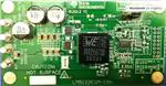
The LM5122 EVM has been designed using a 2-layer board. Most of components are on the top to allow
the user to easily view, probe, and evaluate the LM5122 IC.
Figure 12. Top Silk (Top View)
Figure 13. Bottom Silk (X-Ray View)
Figure 14. Top Copper (Top View)
12
LM5122EVM-1PH Evaluation Module
SNVU197 – APRIL 2013 – Revised AUGUST 2013
Submit Documentation Feedback
Copyright © 2013, Texas Instruments Incorporated
�Bill of Materials
www.ti.com
Figure 15. Bottom Copper (X-Ray View)
9
Bill of Materials
The EVM components are list according to the schematic shown in Figure 11.
Table 3. Bill of Materials
Reference Designator
Description
Manufacturer
Part Number
Qty.
C1, C2, C3, C4
CAP, CERM, 3.3uF, 50V, +/10%, X7R, 1210
MURATA
GRM32DR71H335KA88L
4
C5, C6, C7, C9
CAP CER 10UF 35V 20% X7R Taiyo Yuden
1210
GMK325AB7106MM-T
4
C8
CAP, CERM, 1uF, 50V, +/10%, X7R, 0805
MURATA
GRM21BR71H105KA12L
1
C10, C11, C12
CAP ALUM 330UF 35V 20%
SMD
Panasonic
EEE-FP1V331AP
3
C15
CAP, CERM, 470pF, 100V, +/5%, C0G/NP0, 0805
MURATA
GRM2165C2A471JA01D
1
C16
CAP, CERM, 0.1uF, 25V, +/10%, X7R, 0603
KEMET
C0603C104K3RACTU
1
C17, C19, C20
CAP, CERM, 100pF, 50V, +/5%, C0G/NP0, 0603
MURATA
GRM1885C1H101JA01D
3
C18
CAP, CERM, 4.7uF, 16V, +/10%, X7R, 0805
MURATA
GRM21BR71C475KA73L
1
C22, C23
CAP, CERM, 0.47uF, 25V, +/10%, X7R, 0603
MURATA
GRM188R71E474KA12D
2
C24
CAP, CERM, 0.1uF, 25V, +/10%, X7R, 0603
MURATA
GRM188R71E104KA01D
1
C25
CAP, CERM, 330pF, 50V, +/10%, X7R, 0603
KEMET
C0603C331K5RACTU
1
C26
CAP, CERM, 0.022uF, 50V, +/- KEMET
10%, X7R, 0603
C0603C223K5RACTU
1
R2
RES 0.004 Ω 3W 1% 3015
WIDE
Susumu
KRL7638-C-R004-F-T1
1
R3
RES 8.2 Ω 3/4W 5% 2010
SMD
Vishay Dale
CRCW20108R20JNEF
1
R5, R6
RES, 100 Ω, 1%, 0.1W, 0603
Vishay-Dale
CRCW0603100RFKEA
2
R9, R11, R12, R14,
R18, R30, R32, R33
RES, 0 Ω, 5%, 0.1W, 0603
Panasonic
ERJ-3GEY0R00V
8
R16
RES, 49.9k Ω, 1%, 0.1W, 0603 Vishay-Dale
CRCW060349K9FKEA
1
R17
RES, 3.3 Ω, 5%, 0.1W, 0603
Vishay-Dale
CRCW06033R30JNEA
1
R21
RES, 8.06k Ω, 1%, 0.1W, 0603 Vishay-Dale
CRCW06038K06FKEA
1
SNVU197 – APRIL 2013 – Revised AUGUST 2013
Submit Documentation Feedback
Copyright © 2013, Texas Instruments Incorporated
LM5122EVM-1PH Evaluation Module
13
�Single Output Dual Phase Configuration
www.ti.com
Table 3. Bill of Materials (continued)
10
R22
RES, 100k Ω, 1%, 0.1W, 0603
Vishay-Dale
CRCW0603100KFKEA
1
R23
RES, 36.5k Ω, 1%, 0.1W, 0603 Vishay-Dale
CRCW060336K5FKEA
1
R25
RES, 68.1k Ω, 1%, 0.1W, 0603 Vishay-Dale
CRCW060368K1FKEA
1
R26
RES, 2.67k Ω, 1%, 0.1W, 0603 Vishay-Dale
CRCW06032K67FKEA
1
R27
RES, 49.9k Ω, 1%, 0.125W,
0805
Vishay-Dale
CRCW080549K9FKEA
1
R28
RES, 825 Ω, 1%, 0.125W,
0805
Vishay-Dale
CRCW0805825RFKEA
1
D4
Diode, Schottky, 60V, 1A,
SOD-123F
NXP
Semiconductor
PMEG6010CEH
1
Q2, Q3
MOSFET N-CH 40V 100A
LFPAK
NXP
Semiconductor
PSMN4R0-40YS
2
MOSFET N-CH 40V 100A
SON 5x6
Texas
Instruments
CSD18501Q5A
Alternative
L1
SMD Flat Wire Inductor,
L=10.0 µH
WURTH
74435561100
1
TP1, TP2, TP3, TP4
Terminal, Turret, TH, Double
Keystone
1503-2
4
H1, H2, H3, H4
Machine Screw, Round, #4-40
x 1/4, Nylon
B&F Fastener
Supply
NY PMS 440 0025 PH
4
H5, H6, H7, H8
Standoff, Hex, 0.5"L #4-40
Nylon
Keystone
1902C
4
J1
Header, TH, 100mil, 4x1, Gold
plated, 230 mil
SAMTEC, Inc.
TSW-104-07-G-S
1
SH-J1
Shunt, 100mil, Gold plated,
Black
3M
969102-0000-DA
1
U1
Synchronous Boost Controller
TI
LM5122MH
1
Single Output Dual Phase Configuration
Two LM5122EVM-1PH evaluation boards can be easily configured as a single-output dual-phase
interleaved boost converter following the four steps listed below:
1. Remove C19, C25, C26, R25, R26, R27, R28, R30, and R32 on the slave board.
2. Populate 0Ω resistors (R24 and R31) on the slave board.
3. Populate J2 on both master and slave boards.
4. Connect J2 on the master board and J2 on the slave board together using a flat cable.
14
LM5122EVM-1PH Evaluation Module
SNVU197 – APRIL 2013 – Revised AUGUST 2013
Submit Documentation Feedback
Copyright © 2013, Texas Instruments Incorporated
�IMPORTANT NOTICE
Texas Instruments Incorporated and its subsidiaries (TI) reserve the right to make corrections, enhancements, improvements and other
changes to its semiconductor products and services per JESD46, latest issue, and to discontinue any product or service per JESD48, latest
issue. Buyers should obtain the latest relevant information before placing orders and should verify that such information is current and
complete. All semiconductor products (also referred to herein as “components”) are sold subject to TI’s terms and conditions of sale
supplied at the time of order acknowledgment.
TI warrants performance of its components to the specifications applicable at the time of sale, in accordance with the warranty in TI’s terms
and conditions of sale of semiconductor products. Testing and other quality control techniques are used to the extent TI deems necessary
to support this warranty. Except where mandated by applicable law, testing of all parameters of each component is not necessarily
performed.
TI assumes no liability for applications assistance or the design of Buyers’ products. Buyers are responsible for their products and
applications using TI components. To minimize the risks associated with Buyers’ products and applications, Buyers should provide
adequate design and operating safeguards.
TI does not warrant or represent that any license, either express or implied, is granted under any patent right, copyright, mask work right, or
other intellectual property right relating to any combination, machine, or process in which TI components or services are used. Information
published by TI regarding third-party products or services does not constitute a license to use such products or services or a warranty or
endorsement thereof. Use of such information may require a license from a third party under the patents or other intellectual property of the
third party, or a license from TI under the patents or other intellectual property of TI.
Reproduction of significant portions of TI information in TI data books or data sheets is permissible only if reproduction is without alteration
and is accompanied by all associated warranties, conditions, limitations, and notices. TI is not responsible or liable for such altered
documentation. Information of third parties may be subject to additional restrictions.
Resale of TI components or services with statements different from or beyond the parameters stated by TI for that component or service
voids all express and any implied warranties for the associated TI component or service and is an unfair and deceptive business practice.
TI is not responsible or liable for any such statements.
Buyer acknowledges and agrees that it is solely responsible for compliance with all legal, regulatory and safety-related requirements
concerning its products, and any use of TI components in its applications, notwithstanding any applications-related information or support
that may be provided by TI. Buyer represents and agrees that it has all the necessary expertise to create and implement safeguards which
anticipate dangerous consequences of failures, monitor failures and their consequences, lessen the likelihood of failures that might cause
harm and take appropriate remedial actions. Buyer will fully indemnify TI and its representatives against any damages arising out of the use
of any TI components in safety-critical applications.
In some cases, TI components may be promoted specifically to facilitate safety-related applications. With such components, TI’s goal is to
help enable customers to design and create their own end-product solutions that meet applicable functional safety standards and
requirements. Nonetheless, such components are subject to these terms.
No TI components are authorized for use in FDA Class III (or similar life-critical medical equipment) unless authorized officers of the parties
have executed a special agreement specifically governing such use.
Only those TI components which TI has specifically designated as military grade or “enhanced plastic” are designed and intended for use in
military/aerospace applications or environments. Buyer acknowledges and agrees that any military or aerospace use of TI components
which have not been so designated is solely at the Buyer's risk, and that Buyer is solely responsible for compliance with all legal and
regulatory requirements in connection with such use.
TI has specifically designated certain components as meeting ISO/TS16949 requirements, mainly for automotive use. In any case of use of
non-designated products, TI will not be responsible for any failure to meet ISO/TS16949.
Products
Applications
Audio
www.ti.com/audio
Automotive and Transportation
www.ti.com/automotive
Amplifiers
amplifier.ti.com
Communications and Telecom
www.ti.com/communications
Data Converters
dataconverter.ti.com
Computers and Peripherals
www.ti.com/computers
DLP® Products
www.dlp.com
Consumer Electronics
www.ti.com/consumer-apps
DSP
dsp.ti.com
Energy and Lighting
www.ti.com/energy
Clocks and Timers
www.ti.com/clocks
Industrial
www.ti.com/industrial
Interface
interface.ti.com
Medical
www.ti.com/medical
Logic
logic.ti.com
Security
www.ti.com/security
Power Mgmt
power.ti.com
Space, Avionics and Defense
www.ti.com/space-avionics-defense
Microcontrollers
microcontroller.ti.com
Video and Imaging
www.ti.com/video
RFID
www.ti-rfid.com
OMAP Applications Processors
www.ti.com/omap
TI E2E Community
e2e.ti.com
Wireless Connectivity
www.ti.com/wirelessconnectivity
Mailing Address: Texas Instruments, Post Office Box 655303, Dallas, Texas 75265
Copyright © 2015, Texas Instruments Incorporated
�


 工商网监
湘ICP备2023018690号
工商网监
湘ICP备2023018690号
